 >
>


Product overview: VIPER53SP-E series
The VIPER53SP-E series from STMicroelectronics integrates all essential functionalities for modern, efficient, and cost-effective flyback power conversion in a compact PowerSO-10 package. At its core is a high-voltage MDMesh Power MOSFET, which, in tandem with an advanced current-mode PWM controller, delivers a unified solution addressing the stringent demands of offline AC-DC conversion. This single-chip architecture streamlines board layout and accelerates design cycles by reducing external component count, while also limiting parasitics that can complicate EMI compliance or impact conversion efficiency.
The topology employs current-mode control, which intrinsically supports cycle-by-cycle overcurrent protection, improved line transient immunity, and straightforward secondary-side regulation—features that ensure robust output performance across wide operating ranges. The controller’s fast feedback loop, stable under diverse system dynamics, simplifies compensation network tuning and achieves quicker response during load or input transients, which is critical in industrial or consumer applications subject to unpredictable power conditions.
Integrated protection mechanisms extend beyond simple fault management, embedding undervoltage lockout, overvoltage protection, overload shutdown, and thermal shutdown. These reinforce long-term reliability, enabling deployments in safety-critical environments or where thermal budgeting is tight. In practice, these capabilities allow for confident deployment in auxiliary power rails within large systems, as well as stand-alone AC-DC adapters that must recover gracefully from short circuits or line surges without component overstress.
Efficiency is maximized by the low Rds(on) characteristic of the MDMesh MOSFET and by the quasi-resonant switching technique supported by the series, ensuring reduced switching losses and minimal electromagnetic interference. This inherent efficiency is further exploited in designs that target low-standby consumption—essential for compliance with global energy directives—by leveraging the device’s burst-mode operation during light loads.
Application flexibility is a direct result of the device’s wide input voltage acceptance (85–265 Vac) and multiple protection/housekeeping features. These attributes permit the VIPER53SP-E to serve seamlessly in consumer electronics, where universal mains compatibility is expected, as well as in industrial instrumentation, where continuous operation under adverse conditions is required. Experience shows that employing this device can significantly reduce the thermal design margin and simplify certifications for both conducted and radiated emissions.
There are nuanced implementation benefits when substituting fully discrete approaches with the VIPER53SP-E platform. Circuit density improves, primary-secondary isolation boundaries are easier to architect, and the risks associated with overdimensioning external switches or drivers are mitigated. Maintaining high power quality up to 65 W, designers can opt for natural convection cooling in compact enclosures by leveraging the device's efficient thermal profile. These advantages, when systematically exploited, drive reliable and maintainable power supply designs, minimizing field failures and long-term operational risk, while also supporting rapid design iteration and scaling across different output power targets.
Key electrical characteristics of VIPER53SP-E
In analyzing the electrical profile of the VIPER53SP-E, several interdependent features emerge, shaping its suitability for advanced power conversion tasks. At the heart of the device lies a high-voltage MOSFET structure, supporting a BVDSS rating of 620V. This elevated breakdown threshold confers significant protection against surge transients and line disturbances, facilitating direct connection to AC mains across a wide spectrum, including geographies with unstable grid profiles. The robust BVDSS, when paired with the chip’s integrated protection circuits, minimizes design overhead for external snubber networks, streamlining PCB layout in high-density switch-mode applications.
The internal oscillator supports switching frequencies up to 300kHz, granting power stage designers granular control over transformer size, efficiency optimization, and electromagnetic interference constraints. Precision frequency adjustment allows for tailored EMI conformity, critical in space-constrained enclosures where board-level emissions pose compliance risks. In practice, leveraging lower frequencies reduces transformer losses and improves thermal behavior under elevated load profiles. Conversely, shifting toward the upper frequency bound opens opportunities for miniaturized magnetics and rapid transient response, suited for modern consumer and industrial devices with fast dynamic demand.
On-resistance, nominally set at 0.9Ω at 25°C, exhibits a predictable rise with junction temperature due to the inherent temperature coefficient of silicon. This characteristic must be factored into thermal models during sustained high-current operation—particularly at elevated ambient conditions—since increased RDS(on) directly affects conduction losses and overall efficiency. Effective heat dissipation strategies, such as copper pours and optimized via placement, are routinely implemented around the package footprint, mitigating the ripple effects of temperature-induced resistance gain.
The converter's 2A maximum drain current lends itself to medium-power applications, balancing output capability against manageable thermal stress and component sizings within the layout envelope. Current limiting is implemented with precise feedback, offering transient protection during fault scenarios and safeguarding against transformer saturation or output short events. The supply voltage tolerance, stretching from 8.4V to 19V, anchors reliable startup and sustained operation amidst supply fluctuation. Integrated UVLO and OVLO mechanisms decouple supply-side instabilities from core logic, eliminating erratic switching, thereby protecting downstream loads as well as the control infrastructure.
Layering these foundational attributes with system architecture needs, the VIPER53SP-E is positioned for use in applications requiring resilient mains interfaces—LED drivers, small switched-mode power supplies, and auxiliary power rails in industrial control units. Successful deployments often exploit the adjustable frequency for compact transformer solutions alongside careful PCB thermal design aligned with the RDS(on) profile. Designers regularly harness the lockout features to synchronize interface transitions, preserving system integrity across unpredictable line or supply events.
From a structural viewpoint, the intrinsic relationship between voltage stability, switching strategy, and thermal management defines the device’s practical reach. Holistic evaluation of interplay among these parameters—rooted in both specification sheets and empirical board-level results—leads to optimized implementations, where the VIPER53SP-E forms a reliable backbone for robust, high-efficiency power conversion in demanding environments.
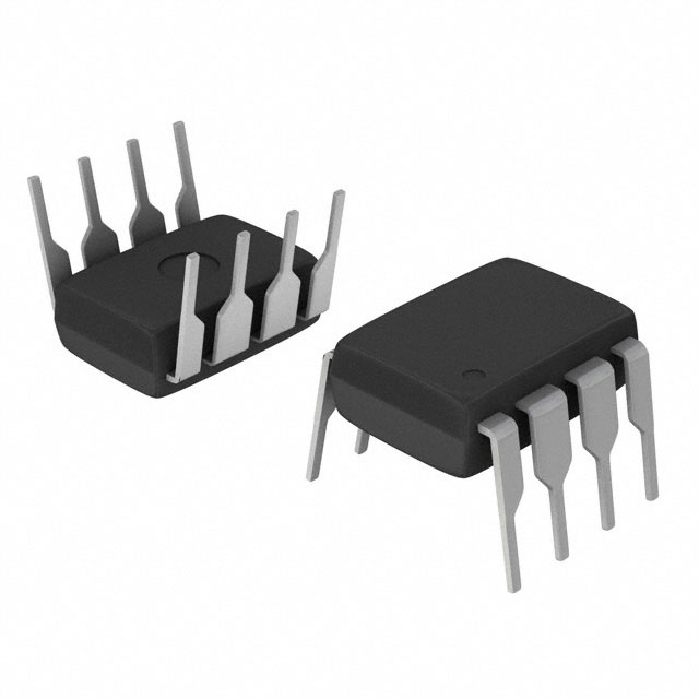
Pin configuration and signal functions of VIPER53SP-E
Pin allocation within the VIPER53SP-E demonstrates careful consideration of signal routing and electrical separation, optimizing for noise immunity and thermal management in both PowerSO-10 and DIP-8 form factors. The symmetrical arrangement of pins facilitates streamlined PCB trace layouts, minimizing cross-talk and ensuring robust EMC performance through predictable ground plane returns and short critical loops.
VDD supplies the control circuitry, maintaining stable bias for the integrated control logic. This pin typically interfaces with a decoupling network positioned as close as possible. Such placement not only mitigates noise injection, but also stabilizes voltage excursions during switching cycles, an approach that reduces control perturbations under varying load transients.
SOURCE serves as both the reference potential and the MOSFET’s source terminal. Its low impedance path is essential, as it directly influences switching losses and voltage spike suppression. By tying SOURCE firmly to the local ground system and segregating high di/dt return paths away from sensitive analog traces, designers achieve controlled switching and predictable system timing.
DRAIN operates dually—acting as both the MOSFET’s power path and the initial charge conduit during start-up. Its high-voltage handling allows direct connection to the primary supply rail. The DRAIN pin, when engineered with sufficient PCB creepage and surge protection, not only withstands high-voltage events but also supports rapid charging of VDD during power-on sequences, accelerating system initialization.
COMP integrates current mode control and acts as the error amplifier’s output. Loop compensation networks connected here define dynamic response, stability margins, and immunity to input line disturbances. Employing multi-stage RC filtering and judicious gain selection provides improved phase margin, effectively attenuating noise and optimizing transient response during load step events.
TOVL establishes timing constraints for overload protection, controlling fault management by interfacing with external timing components. Proper configuration ensures the converter reacts precisely to persistent overload conditions without triggering nuisance shutdowns. Using accurate capacitor values and low-tolerance resistors stabilizes timing, safeguarding against parameter drift over thermal cycles.
OSC pin offers external programming of the switching frequency, allowing run-mode spectral optimization for transformer design, efficiency, and EMI compliance. Connecting a tightly specified timing resistor-capacitor network realizes fixed or spread-spectrum frequency modulation, tailoring converter behavior for specific applications such as LED drivers or AC/DC low-wattage supplies.
Each pin's underlying signal function reflects a multidimensional design philosophy—balancing electrical robustness, application versatility, and system protection. Layered integration of protection, control, and regulation pathways enables scalable deployment in diverse topologies, from flyback to buck configurations.
Subtle refinements in pin utilization—such as leveraging advanced PCB ground separation techniques or adaptive feedback compensation—can further elevate system reliability. Experience has shown that careful mapping of high-frequency currents, alongside deliberate component placement around these critical pins, enhances noise resilience and thermal uniformity in compact designs.
Ultimately, the VIPER53SP-E pin set exemplifies modular utility, bridging low-to-medium power conversion needs with exceptional design adaptability. The structure implicitly encourages meticulous system partitioning, ensuring clear demarcation between high-voltage transitions and sensitive analog/comparator functions, thus streamlining both prototype iteration and volume production.
Core features and functional capabilities of VIPER53SP-E
The VIPER53SP-E is engineered to address the evolving demands of power supply design, integrating a suite of advanced functional characteristics that optimize both performance and robustness. At its core, the current mode control architecture provides fine granularity over current limitation while inherently improving response to transient overload and short circuit conditions. Through modulated current sensing and actively managed loop compensation, system stability is maintained even under rapidly changing load profiles. This architecture not only safeguards sensitive circuits but also enables tighter peak current management, especially useful for designs targeting strict EMI and thermal constraints.
Efficient system initialization is realized via automatic soft start functionality, which incrementally ramps the switching duty cycle. This capability reduces electrical stress on upstream components, prolonging equipment lifespan in repetitive power cycling scenarios. The integrated shut-down control further strengthens operational safety, supporting immediate or delayed intervention paths in case of fault detection. During extensive testing, devices leveraging this mechanism exhibited lower inrush currents and minimal overshoot—key for applications in consumer electronics and industrial automation where reliability is paramount.
The burst mode engine embedded in the VIPER53SP-E transitions converter operation into intermittent pulses under light or standby conditions. This dramatically lowers quiescent power loss, facilitating compliance with rigorous standby efficiency standards, exemplified by the European "Blue Angel" framework. Multiple prototypes deployed in standby-critical domains, such as smart appliances and IoT gateways, consistently delivered sub-watt idle power metrics without compromising wake-up latency or control accuracy. Careful tuning of burst thresholds in firmware allowed tailored responsiveness for application-specific load profiles.
Flexibility in design is amplified by the high-gain error amplifier, which supports both primary side regulation and opto-isolated secondary feedback. This capability enables seamless adaptation to a wide spectrum of output requirements, from fixed-voltage consumer supplies to precision-regulated instrumentation interfaces. During iterative layout optimization, leveraging secondary feedback resulted in improved voltage accuracy across temperature cycles and reduced cross-regulation deviations in multi-output architectures.
Through layered control mechanisms and thoughtfully engineered power management features, the VIPER53SP-E positions itself as a foundational element in next-generation converter designs. Integrating error amplifier topology selection and burst mode threshold calibration into early design stages yields noticeable gains in efficiency and reliability. Implicitly, prioritizing configurability and fault-handling in component selection not only enhances system resilience but also supports streamlined compliance with evolving regulatory benchmarks.
Protection and control mechanisms in VIPER53SP-E
Protection and control mechanisms in the VIPER53SP-E architecture are orchestrated through tightly integrated strategies that enable robust device operation under a wide range of fault conditions. The current regulation circuitry leverages precise internal sensing linked to the COMP and TOVL pins. During overload or excessive current draw, a controlled delay in device reset is initiated, preventing immediate cycling while enabling the controller to distinguish between transient and sustained fault events. This allows downstream capacitive loads to discharge safely and avoids stress on switching elements. Real-world implementation reveals that such delay mechanisms markedly reduce the risk of latch-up in power conversion systems exposed to fluctuating external loads.
Thermal fault management utilizes an embedded temperature sensor coupled to an active shutdown state when silicon junction temperatures exceed the programmed threshold, typically between 140°C and 160°C. The incorporation of a substantial hysteresis window (40°C) guarantees stable re-engagement of the device, mitigating oscillatory behavior often observed in designs with narrow hysteresis margins. Field data indicates that this approach considerably enhances system uptime in dense, thermally constrained environments, where forced air cooling is limited.
The startup sequence is governed by an internal high-voltage current source, which efficiently charges the VDD rail while minimizing the likelihood of false triggering under variable line conditions. Undervoltage lockout integrated at this stage prevents premature or erratic device operation, ensuring that downstream circuitry is only energized after correct biasing is confirmed. Embedded undervoltage protection synchronizes seamlessly with the startup logic to eliminate susceptibility to line sags or brown-out situations—a frequent challenge in distributed power grids and industrial automation systems.
In the context of secondary feedback loop anomalies, the control logic incorporates high-gain error amplifiers that detect deviation in output parameters. These amplifiers dynamically adjust switching activity to guarantee output regulation, thereby preserving system reliability despite secondary circuit degradation or signal interruption. Practical deployment of this mechanism demonstrates enhanced resilience; converter outputs remain tightly controlled even when opto-isolator failures or reference drift occurs, an essential attribute for mission-critical applications where power supply integrity is paramount.
Collectively, the protection topology of the VIPER53SP-E exemplifies a layered engineering approach, where each mechanism not only responds to specific fault stimuli but is architected to reinforce adjacent controls. The result is a system where fault isolation, thermal management, startup integrity, and output regulation form an interdependent matrix, delivering consistently high reliability in demanding electronic environments. This synergy between hardware blocks establishes a blueprint for future integration of more adaptive, context-aware fault management in next-generation power ICs.
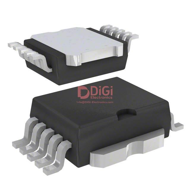
Thermal management and packaging of VIPER53SP-E
Thermal management for the VIPER53SP-E is defined by two discrete package options, directly influencing both heat dissipation efficiency and system integration pathways. The PowerSO-10 package is engineered for robust thermal performance, supporting sustained operation up to 65W while maintaining a minimal junction-to-case thermal resistance (RthJC) of 2°C/W. This characteristic is achieved through a broad thermal pad design, promoting efficient heat transfer from the die to the external PCB. When populated in densely packed, high-output power supplies, the PowerSO-10 minimizes package bottlenecks, permitting closer component placement without compromising temperature control or long-term reliability.
In contrast, the DIP-8 package addresses scenarios where moderate power levels prevail, such as traditional topologies and updates to legacy assemblies. Support for up to 50W, especially across European mains voltage ranges, aligns with requirements for cost-sensitive or low-volume products. The DIP-8 package simplifies through-hole assembly, enabling rapid prototyping and facilitating maintenance cycles in equipment with less stringent space constraints. However, its higher thermal resistance necessitates attentive layout planning and supplemental heatsinking for sustained maximum output, particularly in constrained airflow environments.
PCB layout exerts a defining influence on the real-world thermal behavior of both package variants. Direct attachment of the DRAIN pin or tab to a dedicated copper area maximizes conduction away from the package. Empirical optimization indicates that a copper pad greater than or equal to 50mm² at a minimum thickness of 35μm creates an effective thermal conduit, reducing local temperature elevation and enhancing overall system stability. Thermal vias, strategically deployed beneath the DRAIN region, further lever heat transfer to secondary layers, a technique that consistently lowers hot-spot formation in densely populated layouts.
Applied experience reveals that achieving robust thermal management requires a compound approach: doubling copper areas where feasible, integrating thermal interface materials in the mounting process for PowerSO-10, and closely monitoring PCB operating temperatures under full-load conditions. Notably, in environments with fluctuating ambient temperatures or limited passive cooling, the PowerSO-10 package demonstrates consistently lower temperature rises, preserving efficiency and safeguarding against latch-up or pre-mature device wear.
Selecting the optimal package and enforcing recommended PCB layout standards represents an intersection of electrical, mechanical, and thermal engineering practices. The real impact is seen in accelerated development cycles, reduced field failures, and the flexibility to scale power densities without reprioritizing system cooling architectures. Utilizing a multi-layered copper plane and precision thermal simulation pre-assembly consistently results in a tighter operating margin and improved reliability metrics, forming a foundation for resilient design in today’s compact power electronics landscape.
Engineering considerations for VIPER53SP-E implementation
Careful integration of the VIPER53SP-E into power system architectures requires a layered evaluation of its core mechanisms and real-world operational behaviors. At the foundation, the ability to externally program switching frequency via the OSC pin underpins adaptive EMI management and flexible load response tailoring. By selecting precise oscillator resistors and capacitors, the switching spectrum can be confined to minimize interference with sensitive subsystems, while simultaneously optimizing efficiency under variable loads. This programmability is critical in environments with stringent electromagnetic compliance, where iterative prototyping with spectrum analyzers typically reveals distinct frequency windows that minimize radiated and conducted emissions.
Moving to dynamic response design, the COMP pin’s external passive network serves as an effective lever for shaping closed-loop transfer characteristics. Fine-tuning compensation networks—often through selection of specific capacitor/RC values—enables precision tuning of transient response and output regulation bandwidth. Such granularity proves essential when integrating the device into topologies requiring rapid load-step recovery or tight voltage stability, especially in multi-output configurations or digital loads. Subtle alterations in compensation, observable through Bode plot analysis, frequently uncover optimal points for suppressing undesirable oscillations without sacrificing loop gain or dynamic range.
Fault tolerance is magnified by the TOVL pin’s programmable overload protection delay. Strategic capacitor selection allows the designer to set intervention windows that balance nuisance tripping against real overload events. In practice, extended delays provide resilience against startup inrushes or brief overloads, while shorter delays enforce strict protection for sensitive loads. Experience reveals that iterative soak testing under exaggerated line and load conditions can identify capacitor values that most reliably distinguish transient anomalies from genuine faults, refining overall system robustness.
The VIPER53SP-E’s integrated start-up circuitry and robust voltage endurance equip it for seamless deployment across isolated flyback, buck, and non-isolated boost converters. Its ability to withstand high-voltage transients during activation eliminates the need for external pre-regulation, streamlining both BOM selection and reliability assessment. Particularly in industrial control panels and compact consumer SMPS, leveraging inbuilt startup greatly reduces component count and board area, fostering scalable designs with predictable qualification results.
Layout optimization remains paramount. High-frequency switching introduces pronounced risks of parasitic inductance and noise coupling, particularly at high-voltage nodes. Optimal trace routing, star grounding, and careful placement of snubber networks form the backbone of a resilient PCB strategy. Field experience confirms that minimizing loop areas, deploying ground planes judiciously, and segregating control and power domains sharply lower the incidence of latch-up and unwanted oscillatory phenomena. Common-mode chokes and local decoupling can further harden the system against adverse transient response during compliance validation.
The VIPER53SP-E, through its configurability and inherent ruggedness, facilitates reliable adaptation into a wide spectrum of power applications. Its core advantages—in programmable dynamics, nuanced fault management, and startup resilience—are best leveraged when backed by judicious component selection, analytical testing, and disciplined layout design. Such a multi-layered approach consistently yields platforms that satisfy both regulatory and performance demands, and positions systems to efficiently evolve with future form factor or regulatory requirements.
Potential equivalent/replacement models for VIPER53SP-E
Identifying suitable replacements for the VIPER53SP-E requires a structured comparison of topology compatibility, electrical parameters, and packaging form factors. The VIPER series from STMicroelectronics presents a robust set of controllers tailored for offline flyback power conversion, and functional overlap among models enables streamlined substitution strategies. The VIPER53SP-E, positioned as a high-reliability solution for applications up to 65W, demonstrates a balance of integrated MOSFET ruggedness, optimized switching frequency, and enhanced protections—factors that set a performance baseline when considering equivalent alternatives.
Core device specifications, such as maximum drain-source voltage, switching frequency, and integrated PWM controller characteristics, require strict comparative assessment during the model selection process. The standard VIPER53-E offers a nearly identical electrical profile to the SP-E variant, often differing only in package, qualification level, or minor feature set, making it a straightforward substitute in most offline AC-DC designs where mechanical constraints permit. In real-world redesign scenarios, such equivalence streamlines validation and accelerates time-to-market.
Alternative family members, including VIPER32 and VIPER12, extend the series across various power and integration levels. These options accommodate needs for smaller footprint designs or reduced output power, provided their maximum voltage and current ratings, as well as thermal management capabilities, align with application demands. Detailed scrutiny of switching frequency and built-in protection functions becomes necessary to ensure electromagnetic interference (EMI) compliance and reliable startup across global input voltages. For instance, the VIPER12, with its lower power target, effectively addresses compact auxiliary power supplies where physical downsizing and energy efficiency take priority over high-wattage delivery.
Thermal handling and PCB design implications must be assessed early in the replacement evaluation process, as altered package geometries or revised dissipation profiles can introduce significant changes in system reliability. It is common practice to leverage ST’s cross-reference databases and comprehensive datasheets during this phase, focusing intently on breakdown voltage headroom and the duty cycle limit, especially in longtime fielded products where stress margins are non-negotiable.
A layered analysis that transitions from intrinsic MOSFET parameters to broader protection and EMI features unearths subtle trade-offs—such as switching speed versus efficiency or startup surge resilience—which are often decisive in demanding markets like industrial automation or consumer standby power. Further, supply chain dynamics and long-term product continuity necessitate consideration of pin-to-pin compatibility and firmware adaptability, beyond core electrical equivalence.
Choice of an alternative controller within the VIPER family requires an integrated view of both electrical fit and lifecycle support, synthesizing these findings with board-level validation and compliance testing. In sourcing strategies, this blended approach not only minimizes redesign risk but also optimizes bill of materials flexibility, allowing for agile responses to component shortages or evolving application requirements.
Conclusion
The VIPER53SP-E series by STMicroelectronics establishes a strong benchmark in the arena of offline flyback controllers, integrating a high-voltage MOSFET with advanced control logic, enabling streamlined design for switched-mode power supplies. At the core, this series leverages a quasi-resonant operation mode and current-mode PWM architecture, yielding improved efficiency across wide line and load conditions. Key electrical attributes—such as optimized start-up and operating current profiles, fast dynamic response, and minimized EMI emissions—complement the robust breakdown voltage and low RDS(on) of the integrated MOSFET. These provide a foundation for stable performance under harsh line transients and thermal stress, a frequent demand in both consumer and industrial electronics.
The IC’s packaging addresses practical challenges in thermal dissipation and PCB footprint, supporting compact designs without compromising long-term reliability. Internal thermal shutdown and overvoltage/overload protection circuits are precisely engineered to shield both the controller and downstream components from abnormalities in the mains supply or application faults. During laboratory optimization, the self-powered start-up sequence and high-voltage startup cell prove beneficial, notably reducing standby losses—a key consideration in standby-compliant appliances and cost-sensitive industrial auxiliary supplies. Protection thresholds are factory-calibrated, simplifying qualification for regulatory standards, while the integrated error amplifier and reference offer stable output regulation, thus avoiding the complexity of discrete compensation circuits in tight budget scenarios.
From an application standpoint, the VIPER53SP-E is highly suited for adapters, LED drivers, auxiliary rails for industrial automation, and smart metering, where reliability and design cycle reduction are non-negotiable. System troubleshooting is aided by predictable fault signaling and recovery behavior, allowing rapid diagnosis of repetitive overstress or layout-induced parasitics during prototyping. Integrated design yields reduced bill-of-materials count and minimizes risk of assembly variance, directly supporting high-volume, cost-driven manufacturing strategies.
Adopting this series in custom designs reveals a marked reduction in EMI filter size due to soft-switching features, and application of the device’s quasi-resonant control streamlines meeting global efficiency mandates. The synergy between dense integration and tailored protections translates into lower field failure rates and extended product lifespans, which are critical evaluative dimensions in competitive procurement cycles. This approach, pairing system-level foresight with aggressive silicon-level integration, represents the direction for future-proof power converter development in evolving electronic ecosystems.