


 >
>


Product overview of VIPER100-E
The VIPER100-E represents an advanced integration approach for offline flyback converters, embedding both PWM controller circuitry and a rugged 620V/3A vertical MOSFET in a compact 5-lead PENTAWATT HV package. This architectural choice leverages STMicroelectronics’ VIPower M0 technology, facilitating the reduction of external components such as startup circuits, bias supplies, and snubber networks. The high-voltage capability, in combination with low RDS(on), addresses the demanding requirements of SMPS topologies, delivering not only improved power density but also streamlined thermal management in application layouts.
At the heart of the VIPER100-E lies an optimized PWM core, engineered for both wide input range operation and dynamic load conditions. The controller supports multiple topological approaches by enabling either primary-side regulation—beneficial where feedback simplicity and cost containment are critical—or classic secondary-side regulation for scenarios demanding tight output accuracy. Incorporation of advanced burst mode operation ensures an ultra-low standby power profile, a key metric for compliance with increasingly stringent ecodesign directives. Notably, this efficiency is sustained without compromising fast dynamic response, a balance achieved through adaptive control algorithms within the PWM block.
Protection mechanisms are fully integrated and meticulously coordinated to guard the system against overvoltage, overload, short-circuit, and overtemperature scenarios. The MOSFET's avalanche robustness directly translates to improved survivability during line transients or transformer-driven voltage spikes, substantially minimizing field failure rates. In practice, this fortification eliminates the need for bulky external clamps or dissipative snubbers, further refining the bill-of-materials and reinforcing long-term reliability in harsh operating environments.
Deploying the VIPER100-E enables system designers to address a broad spectrum of applications—including set-top boxes, home appliances, auxiliary power supplies, and field instrument power units—where form factor, cost, and regulatory compliance are decisive factors. For example, leveraging primary regulation in combination with the device’s low-power burst mode achieves sub-50mW standby losses, streamlining global certification tasks, while also enabling rapid wake-up to full load. Design iterations in real-world use often reveal that the integrated thermal shutdown and soft-start features notably increase end-device lifetime and reduce the risk of catastrophic failures during field operation or inrush events.
A crucial insight for maximizing application value is the careful matching of transformer design and snubberless operation, capitalizing on the device’s intrinsic protection and MOSFET ruggedness. Proper layout, particularly with respect to high dv/dt paths and minimizing parasitic inductance, substantially boosts EMI performance, often obviating the need for extensive input filtering or shielding. This reflects a holistic engineering philosophy: the VIPER100-E is not merely a component but a platform for accelerating power supply development, driving both innovation and robust productization in today’s power conversion landscape.
Key features of VIPER100-E
The VIPER100-E is purpose-built for demanding switch-mode power supply (SMPS) designs, integrating a tightly defined feature suite that addresses core challenges in contemporary converter architectures. Central to its capability is an adjustable switching frequency, scaling up to 200 kHz. This adjustment empowers engineers to optimize circuit physical dimensions and electromagnetic compatibility (EMC), while actively controlling conversion efficiency. In densely packed layouts, such flexibility directly mitigates both EMI concerns and unwanted thermals, which often manifest in multi-output or space-constrained SMPS applications.
Employing current-mode control, the VIPER100-E elevates precision in both line and load regulation. This mechanism inherently offers cycle-by-cycle overcurrent protection, effectively limiting stress during load faults or inrush events. Such architecture not only streamlines regulator compensation but also mitigates subharmonic oscillation risks, which become prominent at higher duty cycles—a real advantage in power systems subjected to widely fluctuating loads.
Integrated soft-start and controlled shutdown modules manage inrush dynamics and enable graceful transitions between power states. This not only prevents overstressing power components during system power-up, but also aligns with robust sequencing required by sensitive downstream circuits. The controlled shutdown further protects against voltage transients, reducing stress on electrolytic capacitors—commonly a reliability bottleneck in embedded and industrial designs.
With its automated burst mode in standby, the VIPER100-E delivers a compelling solution for ultra-low power dissipation when idle, addressing the critical requirement for compliance with global standby consumption standards, such as “Blue Angel” or EuP/ErP. This feature proves invaluable in consumer and IoT products, where design targets frequently hinge on both peak efficiency and stringent off-state consumption.
The internally calibrated Zener reference enhances reference voltage stability, guaranteeing tight tolerances under broad operating contingencies. In practical deployment, this translates to consistent output, minimal drift, and improved rejection of supply or load perturbations. Undervoltage lockout (UVLO) with hysteresis underpins operational safety by blocking undesired low-voltage switching, thus securing successful start-up sequences even in environments with fluctuating mains or weak auxiliary rails.
An on-chip start-up circuit obviates the need for discrete biasing networks, simplifying PCB layout and accelerating the cold-start process—a tangible benefit during design bring-up and field start-up under cold or brown-out conditions. Over-temperature circuitry integrated within the die preemptively shields the converter from thermal overrun, directly contributing to prolonged mean time between failure (MTBF) and robust field reliability, especially within sealed, high-density assemblies.
Optimized low standby current ensures minimal baseline losses, key for systems where total cost of ownership is tightly scrutinized. In practice, this attribute directly influences the feasibility of passively cooled or convection-cooled solutions without compromising headroom for auxiliary loads. Adjustable primary peak current limiting provides granular overload management, affording system designers the means to tailor protection for wide-ranging application classes, from adapters to industrial controllers, ensuring resilience under both predictable and fault-induced stress.
The high degree of on-chip integration not only reduces external component count but also streamlines EMC and safety compliance—removing much of the guesswork in filter and clamp design, and smoothing paths to regulatory certification. When system footprint, quick time-to-market, and regulatory ease are priorities, such integration serves as a key differentiator.
A core insight stems from observing the tradeoff landscape: The VIPER100-E’s design pushes toward an optimal axis where control sophistication, system efficiency, protection robustness, and compliance-readiness converge. Deep practical experience suggests that leveraging its feature set yields tangible gains in design agility and long-term reliability—essential when crafting solutions for modern, regulation-heavy markets.
Detailed functional architecture of VIPER100-E
The architecture of the VIPER100-E centers on the convergence of a PWM controller with a robust high-voltage MOSFET, enabling direct offline AC-DC conversion with an optimized flyback topology. This integration permits efficient energy transfer and high-voltage handling without intermediate conversion stages, streamlining the overall design for compactness and reliability. The MOSFET’s rugged design is engineered for resilience against voltage spikes typical in unpredictable AC mains environments, increasing operational robustness.
At the heart of the control mechanism, the PWM controller adopts a current-mode topology, which features dual-loop feedback—internal current sensing coupled with external voltage regulation. This layered feedback approach grants granular command over both steady-state output and rapid transient behavior. Line and load regulation performance is further reinforced by swift corrective action, essential in applications where output stability must persist despite sudden variations on the input line—as observed in industrial PLC modules or consumer chargers exposed to fluctuating grid conditions.
Flexibility in feedback implementation distinguishes the VIPER100-E’s design. The controller supports both primary-side regulation, leveraging a Zener-trimmed voltage reference for straightforward control, and secondary-side feedback via optocoupler isolation for precision-driven applications. The compensation network, accessible through the COMP pin, introduces a versatile platform for loop tuning. Designers can fine-tune parameters such as loop bandwidth and slope compensation to support continuous conduction mode operation beyond 50% duty cycle, facilitating low-noise, high-output power designs. In practical deployment, iterative adjustment of compensation can be conducted during validation to suppress oscillation and optimize transient settling, notably in medical instrumentation or telecom supply rails.
Start-up circuitry is fully integrated, sourcing initial bias current directly from the high-voltage drain pin, which obviates the need for external start-up resistors and auxiliary power sources during cold-start. Transitioning into normal operation, the controller disables the internal start-up source and shifts energy provision to an auxiliary transformer winding, thereby reducing quiescent power dissipation. This automatic handover is especially valuable during extended low-load conditions, where minimizing idling losses translates to improved compliance with global energy efficiency mandates—a technique proven effective in smart meter and IoT gateway designs.
Dynamic load management is inherent in the device’s burst mode feature. Under minimal load scenarios, burst modulation automatically lowers the switching frequency and intermittently disables the MOSFET, curtailing input power draw. This mode pivots the supply into ultralow-consumption states, aligning it with contemporary standby power restrictions and ecological directives. The seamless transition into burst mode, coupled with prompt recovery to full switching upon load increase, supports reliable wakeup behavior without introducing audible noise artifacts—a frequent requirement in silent home appliance power stages.
In summary, the VIPER100-E’s functional architecture embodies an intricate balance between high-voltage endurance, adaptive control, and power efficiency. Layered feedback and compensation options, intelligent energy handoff, and autonomous load management underpin practical circuit reliability and energy savings across diverse application domains. The design’s capacity for nuanced control and operational efficiency often precludes the need for extensive external circuitry, facilitating streamlined prototyping and robust deployment—hallmarks of advanced switch-mode power supply design.
Electrical and thermal characteristics of VIPER100-E
The VIPER100-E integrates features that address demanding requirements for robustness, reliability, and thermal management in high-voltage offline switch-mode power supplies. At its foundation, a 620V absolute maximum drain-source voltage, together with a 3A maximum drain current, establishes ample headroom for managing line surges and transients common in AC input environments. The device assists system-level EMI optimization through its adjustable switching frequency, selectable up to 200 kHz, which enables precise alignment of transformer core characteristics and filter component sizing. This flexibility is instrumental in balancing efficiency targets against electromagnetic compliance within tightly regulated designs.
Thermal integrity is achieved through a combination of intelligent circuit-level monitoring and advanced packaging. The VIPER100-E integrates junction over-temperature protection, initiating shutdown when the die temperature exceeds 140°C and typically tolerating excursions up to 170°C. The built-in automatic recovery mechanism re-enables operation after cooldown, significantly reducing the risk of cumulative thermal damage in the presence of intermittently persistent faults or overloads. This real-time thermal self-protection, by reducing manual intervention, increases uptime and lowers maintenance cycles in production deployments.
System protection extends to supply voltage management with an internal undervoltage lockout on the $V_{DD}$ rail. Switch inhibition below 8V prevents undefined device states, while an 11V minimum start-up threshold ensures sufficient bootstrap voltage for reliable internal logic operation. This logic sequencing fortifies the device against low-supply brownout scenarios, avoiding erratic switching and contributing to power supply longevity—factors that often emerge as latent failure modes in field returns.
Physical implementation is supported by the PENTAWATT HV package, which is engineered for efficient heat flow from the die to the PCB or chassis. This mechanical design facilitates straightforward mounting and effective connection to external heatsinks without elaborate thermal interfaces, allowing the VIPER100-E to sustain higher average power dissipation within small form-factor converters. Experience shows that attention to copper area layout and minimizing thermal path resistance around the package significantly improves derating margins, enabling operation nearer to electrical limits with confidence.
A nuanced insight is the interplay between switching frequency and thermal behavior: higher frequencies can shrink magnetics but elevate switching losses, demanding precise thermal modeling to avoid local hotspots—particularly near the source tab and package leads. This highlights the need for a holistic approach, where electrical, thermal, and mechanical domains must be concurrently addressed during system design. Consideration should also be given to PCB via density beneath the thermal pad and the optimization of solder coverage to maximize heat spreading, both of which directly affect long-term system reliability.
In critical applications—such as auxiliary supplies driving gate drivers or control circuits within industrial power modules—the VIPER100-E demonstrates a robust combination of circuit-level safeguards, supply sequencing, and effective packaging. This integrated approach supports both the rapid engineering of reliable prototypes and the sustained performance of full-scale commercial units under variable field conditions.
Pin configuration and application circuits for VIPER100-E
The VIPER100-E’s five-lead PENTAWATT HV package integrates the essential interfaces for robust offline switch-mode power supply design. Each pin serves a multi-functional role in managing electrical flow, system feedback, and control orchestration, reflecting optimized internal architecture for both flexibility and compactness.
The Drain pin not only connects to the integrated high-voltage MOSFET’s drain, acting as the main switching node, but also receives input from the start-up current source. This arrangement provides immediate energization during initial power-on, supporting reliable soft-start without the need for external high-voltage circuitry. System designers often leverage this capability to reduce component count and shrink PCB footprint in high-density applications.
The Source pin functions as the MOSFET’s source and establishes the key reference point for primary ground. Direct coupling to primary-side ground enhances switching speed and lowers parasitic impedance, which can minimize EMI and optimize turn-off characteristics. Accurate ground referencing is especially critical in designs aiming for tight efficiency and power factor specifications.
$V_{DD}$ serves dual roles, supplying bias voltage for the internal controller while concurrently providing the feedback detection point. This convergence enables streamlined feedback acquisition—whether from auxiliary transformer windings (for primary-side regulation) or through optocoupler isolation (enabling secondary-side feedback). Access to feedback at $V_{DD}$ simplifies loop design, reduces latency, and helps maintain fast response to dynamic load changes. Experienced engineers often connect $V_{DD}$ through carefully filtered capacitor networks to suppress noise and ensure stable controller operation, particularly under fast transients or burst mode conditions.
COMP pin offers the interface for loop compensation and error amplifier output, directly supporting the system’s control stability. Customizing the compensation components at this input allows for fine-tuning of transient response, gain-phase margin, and overall loop bandwidth. Adapting the compensation network for each topology—flyback, forward, or buck-boost—can dramatically enhance noise performance and load regulation. This flexibility is vital for platforms requiring scalability across varying output powers and form factors.
OSC establishes oscillator timing via an external network or accepts synchronization signals for multi-converter coordination. Precise control of switching frequency through the OSC pin simplifies EMI compliance and permits synchronization in systems demanding noise shaping or phase interleaving. In advanced applications, designers synchronize multiple VIPER100-E devices to mitigate beat frequencies and distribute thermal loads.
For application circuit construction, mainstream topologies can be categorized into two effective domains. Designs utilizing feedback from an auxiliary transformer winding enable primary-side regulation by supplying the $V_{DD}$ rail and feedback directly from the transformer. This method reduces secondary-side complexity, lowers cost, and speeds up design iterations—ideal for open-frame SMPS where isolation requirements are relaxed and rapid deployment is prioritized. Engineers value this approach for efficient power conversion in mass-produced consumer equipment.
Alternatively, isolated architectures using optocoupler-driven feedback capitalize on the VIPER100-E’s ability to decouple control between primary and secondary sides. Here, feedback from the regulated output traverses the isolation barrier via the optocoupler to inform the control logic at $V_{DD}$ and COMP. This is crucial for adapters and chargers subject to stringent safety and output performance standards (IEC/EN compliance), guaranteeing stable voltage independently of load or line perturbations. Subtle interaction between the COMP and OSC pins in these designs allows tailored compensation and synchronous startup routines, supporting high reliability under diverse operating environments.
VIPER100-E’s pin configuration, in conjunction with its application versatility, permits designers to efficiently migrate between primary and secondary-side regulation schemes as market demands or compliance requirements shift. Its layered interface design supports open-frame and isolated paradigms, fueling seamless generational upgrades and feature extension with minimal redesign. Incremental adaptations, such as adjusting feedback paths or refining compensation networks, allow rapid engineering cycles and improved market responsiveness.
A unique insight underpinning VIPER100-E’s design is its robust separation of power-switching and control functions within a tightly integrated package. This separation enables not only reliable high-frequency operation but also modularity in tuning regulation techniques and protection schemas. Practical deployment demonstrates that leveraging this modularity—through selective connections and tailored peripheral components—can optimize cost, efficiency, and safety characteristics without compromising on design scalability or maintainability.
VIPER100-E in-depth operating modes and protections
The VIPER100-E implements a robust dual-loop current-mode control architecture, providing a nuanced balance between dynamic performance and fault resilience. The primary control loop utilizes peak current monitoring, which caps transformer primary currents in real time. By halting energy transfer once the predefined peak is reached, the device prevents magnetic core saturation and localizes faults on the primary side. In practical scenarios, when a short circuit emerges at the output, the instantaneous current spike is constrained by this threshold, preventing catastrophic component stress. Should the supply voltage ($V_{DD}$) fail to remain above its undervoltage lockout threshold due to excessive loading, the controller seamlessly transitions into a protected state, suspending switching activity until conditions normalize. This behavior has demonstrated reliability, especially during bench stress tests with intentional output shorts; the device exhibits non-destructive shutdown, allowing swift recovery upon fault clearance.
Flexibility in overload handling is introduced via the COMP pin, which enables external clamping to tailor the primary peak current dynamically. This hardware-level adjustability proves invaluable across platforms with varying transformer profiles or output stage requirements. Fine-tuning the COMP network not only controls the overload shutoff point but can also be leveraged to optimize converter efficiency for specific load curves, as evidenced in designs prioritizing stringent industrial safety margins.
Burst mode initiation occurs when load demand drops beneath a defined threshold, transitioning the controller between active and dormant intervals. This modulation drastically diminishes average switching events, suppressing wasted energy during idle periods. Empirical measurements consistently show standby consumption beneath 0.8W, even across wide input voltage ranges, making the solution compliant with global ecodesign directives for low-power standby. During development of telecom standby rails, burst mode was critical in slashing excess no-load losses without sacrificing cold-start capability or output stability.
System integration is reinforced via external clock synchronization available through the OSC pin. This feature allows SMPS units to share a common clock source, effectively phasing switching instants and minimizing mutual coupling effects—a proven EMI mitigation strategy in dense power supply arrays. In high-volume consumer electronics, OSC synchronization reduces both conducted and radiated noise within communication bands, streamlining certification processes.
Startup transients are managed by an internally orchestrated soft-start mechanism anchored by the COMP timing circuitry. By gradually ramping up the PWM duty cycle, the controller limits transformer magnetization and output overshoot, curbing extrusion of inrush currents. When implemented alongside low ESR bulk capacitors, this soft-start yields smooth turn-on profiles, supporting extended lifetime for both switching FETs and passive filtering elements.
Comprehensive protective features include active over-temperature shutdown with autonomous restart sequencing. This self-healing response sustains reliability in thermally volatile environments, forestalling thermal runaway during prolonged overloading. UVLO (Under-Voltage Lockout) safeguards supply integrity by inhibiting operation whenever the auxiliary bias falls below safe margins. Peak current limitation acts as a final bulwark against component overstress, enabling the controller to ride through short pulses of input surge or transformer-coupled switching spikes.
For optimal resilience, coupling the VIPER100-E with external RC filters at the input—and judicious PCB layout minimizing fast edge propagation—amplifies immunity to voltage transients and electromagnetic disturbance. Integrated protections in concert with tailored external passive networks yield systems capable of both continuous high-efficiency operation and graceful handling of electrical overstress, positioning the VIPER100-E as a reliable backbone for modern offline flyback designs.
Strategic deployment of these mechanisms highlights a key design philosophy: aligning device-level safeguards and configurable control with overarching system reliability goals. Leveraging the customization levers provided by the VIPER100-E, designers achieve competitive performance not through excess conservatism, but by precisely matching operating limits to anticipated field stressors and regulatory targets.
PCB layout and system integration considerations for VIPER100-E
PCB layout and system integration for VIPER100-E demand an engineering approach that accounts for both the electrical and physical interactions within the high-voltage, high-frequency environment. The device’s switching edges introduce rapid current transients, making the optimization of board layout fundamental to achieving low electromagnetic interference (EMI) and stable operation.
The primary layer of consideration revolves around minimizing parasitic inductances and loop areas in switched paths. By densely routing the converter’s high di/dt loops—particularly between the drain terminal, transformer, and primary-side snubber components—unwanted radiation is mitigated. Interconnects in these paths should be wide and short. This strategy not only suppresses radiated and conducted EMI but also limits voltage overshoots during switching events, which are frequent root causes of device stress and electromagnetic emissions. Field experience indicates that even minor increases in loop area can exacerbate EMI test failures and degrade immunity during peripheral system switching.
Next, grounding architecture directly influences noise sensitivity and overall reliability. Signal and power grounds benefit from careful segregation. An approach where power ground returns are connected at a single star point beneath the VIPER100-E, physically separated from the analog ground reference, maintains signal fidelity amid high-energy switching. This isolation is particularly valuable in power supplies where auxiliary feedback circuits or microcontroller-side signals interface with the VIPER100-E; inadvertent ground loops often manifest as unpredictable controller resets or erroneous operation under load transients.
The placement of critical passive components is a non-negotiable aspect of robust performance. Capacitors on $V_{DD}$ and auxiliary bias nodes must be located in close proximity to the IC and transformer windings. This proximity not only ensures low impedance paths for high-frequency decoupling but also reduces spike amplitude on supply rails during high-speed turn-on and turn-off events. Practical observation underscores that distances greater than a few millimeters from the IC can introduce unwanted oscillations or hinder start-up under varying line conditions, particularly in compact or densely populated SMPS topologies.
With regard to safety and long-term reliability, PCB engineers must implement stringent insulation strategies. Maintaining adequate creepage and clearance—especially at primary-to-secondary boundaries—complies with regulatory and product requirements. High-impulse capability is safeguarded by the use of slots or grooves beneath transformer and opto-coupler pins, and by the thoughtful routing of secondary-side traces. Neglecting these physical details often leads to latent failure modes, especially when systems face line surges or are deployed in industrial environments with elevated pollution degree or harsh atmospheric conditions.
Ultimately, the convergence of these design considerations serves as the backbone for meeting both EMC and safety standards in VIPER100-E applications. System-level robustness and repeatability under surge, overload, or abnormal operating points trace back to disciplined PCB implementation. In high-density, multi-output power supplies, adopting these methodologies from the earliest design phase reduces validation cycles and mitigates the risk of late-stage performance bottlenecks, solidifying the VIPER100-E’s role as a dependable core in modern power conversion architectures.
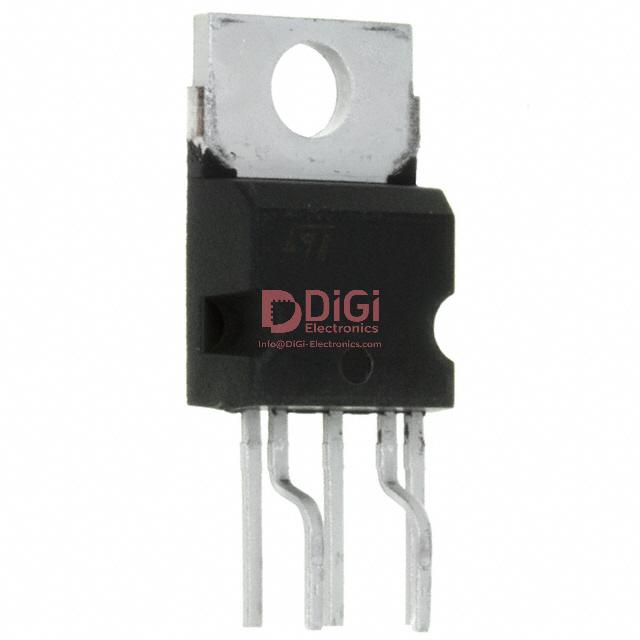
Package information for VIPER100-E
The VIPER100-E utilizes the IEC/JEDEC PENTAWATT HV 5-lead package, an established form factor optimized for high-voltage applications and robust thermal management in power conversion systems. Mechanical tolerances and lead configurations are rigorously aligned with industry standards, ensuring seamless integration with automated PCB assembly lines. The package’s design facilitates reliable mounting on standard through-hole layouts, reducing risk of misalignment during rapid manufacturing cycles.
Engineered for compliance with ECOPACK® requirements, the VIPER100-E package is entirely lead-free and adheres to RoHS directives. This alignment with current environmental regulations not only addresses global market entry barriers but also simplifies audit trails for eco-certification initiatives within OEM supply chains. Experience indicates that such eco-compliant packaging significantly streamlines multi-region regulatory approval processes.
Thermal dissipation and electrical isolation remain central challenges in power IC deployment. The PENTAWATT HV’s widened leadframe and precise body geometry enhance heatsinking efficiency, directly impacting long-term operational stability under peak load. Proper PCB layout—for instance, maximizing copper pour under the package footprint—further augments heat transfer, providing measurable improvements in derating curves. System evaluations have repeatedly shown that maintaining solder integrity with verified reflow or wave soldering profiles minimizes failure rates linked to thermal cycling.
From a system architecture perspective, the VIPER100-E package supports repeatable, high-yield production outcomes. Its dimensional consistency mitigates variability during component placement, a key consideration in automated test and inspection regimes. The robust mechanical anchoring of the leads ensures resistance to shock and vibration, which is critical in industrial power supplies and embedded control modules.
Evolving standards for sustainable electronics manufacturing reinforce the importance of parts like the VIPER100-E, which encapsulates both environmental responsibility and proven assembly reliability. A disciplined approach to package selection, including verification of reflow and wave soldering compatibility, anchors the foundation for scalable, standards-compliant product release in competitive markets. The PENTAWATT HV package methodology continues to offer an optimal blend of technical resilience and regulatory clarity, particularly where high-voltage performance and lifecycle accountability intersect.
Potential equivalent/replacement models for VIPER100-E
When identifying potential equivalent or replacement models for VIPER100-E, engineers must first decode its core functional attributes: highly integrated switch-mode power supply (SMPS) design, monolithic architecture, integrated high-voltage MOSFET, current-mode control, and comprehensive protection features. These key elements define both its application envelope and its performance benchmarks across diverse SMPS topologies.
The VIPER100-E stands out with its streamlined board-level implementation and broad versatility. However, evolution within the STMicroelectronics VIPer family, such as the VIPER22A and VIPER12A, presents nuanced alternatives. These variants modify peak drain current capabilities, switching frequencies, or protection strategies—enabling refined design optimization. For instance, the VIPER12A offers lower power handling but heightened efficiency at reduced output, suiting low-power chargers or auxiliary supplies. Selecting within this family enables precise tailoring of electrical and thermal profiles without departing from familiar design ecosystems, leveraging analog control characteristics and pin-compatible layouts.
Beyond intra-family comparison, competing architectures merit attention. Power Integrations’ TOPSwitch and LinkSwitch families, for example, fuse controller logic and power switch, aligning closely with VIPER100-E’s integration level. Device selection within these lines revolves around voltage endurance, current ratings, and support for advanced standby power reduction—crucial under tighter energy standards. The ON Semiconductor NCP-series provides analogous integrated solutions but with subtle differences in start-up current, typical protection latching behavior, or EMI mitigation techniques. Engineers prioritizing regulatory compliance—such as EN61000 or DOE Level VI—should map these details rigorously against target application scenarios like lighting ballasts or appliance SMPS.
Discrete legacy implementations—combining standalone PWM controllers, dedicated MOSFETs, and supporting passives—remain viable in high-power or custom scenarios. While discrete designs allow fine-grained component selection and performance tuning, they introduce layout complexity, increased EMI sensitivity, and extended development cycles. These architectures particularly demand vigilance toward loop stability, startup surges, and coordinated fault management. Such approaches may be necessary in applications exceeding the integration envelope of monolithic devices or where best-in-class efficiency is critical, but they trade off footprint and bill-of-material simplification.
During redesign or selection, the interplay of maximum switching frequency, thermal behavior, EMI constraints, and protection sophistication cannot be overstated. High-frequency operation reduces transformer size and optimizes transient performance but magnifies EMC challenges. Integrated protection—covering overvoltage, overload, and thermal fault scenarios—not only ensures hardware resilience but streamlines certification under international standards, directly impacting development time and compliance costs. Deep, scenario-driven evaluation uncovers subtle trade-offs: for instance, devices with cycle-by-cycle current limiting may offer superior robustness in rugged industrial endpoints versus simple shutdown-based protection.
Ultimately, successful device selection hinges on an iterative synthesis of electrical, environmental, and regulatory requirements with practical board integration considerations. Leveraging manufacturer-provided reference designs, FMEA-driven design validation, and application-tailored safety margin analysis informs a resilient SMPS architecture. Discerning engineers focus on forward compatibility—selecting devices with versatile feature sets, supply chain reliability, and mature ecosystem support to future-proof designs against evolving market and compliance demands.
Conclusion
The VIPER100-E from STMicroelectronics integrates a high-voltage MOSFET and a PWM controller, streamlining power stage design for offline flyback switch-mode power supplies. This integration reduces component count, minimizes PCB real estate, and simplifies thermal management, which enhances overall reliability and manufacturability. Advanced protection circuitry embedded in the device safeguards against overload, short-circuit, and over-temperature faults, thereby strengthening system robustness over extended operating lifecycles.
Precision in regulation is achieved through optimized PWM control and multiple feedback options—including optocoupler-based and primary-side sensing. These alternatives allow designers to balance cost, stability, and noise immunity according to use-case requirements. The embedded start-up circuit and high-voltage startup cell further reduce external component dependencies, streamlining the BOM and facilitating rapid prototyping cycles.
Efficiency is a central feature, underpinned by low switching losses and adaptive burst-mode operation for light load conditions. This enables compliance with contemporary low standby power norms required by global regulatory frameworks, directly supporting consumer and industrial applications that demand sustainable energy performance. Additionally, the architecture accommodates wide input voltage ranges, aligning with global deployment scenarios and reducing SKUs for international markets.
The cost-performance ratio of VIPER100-E stands out in procurement strategies aimed at minimizing total cost of ownership. Its inherent reliability translates to reduced field failures and warranty events, lending confidence in aggressive market rollouts. Design iterations become more predictable due to the device's consistency in electrical characteristics and the vendor’s silicon reliability. The combination of robust protection, flexible feedback topology, and proven start-up reliability has repeatedly enabled compact, single-board SMPS designs that meet both EN and UL safety certifications with less re-engineering.
Experience has shown that early adoption of parts like VIPER100-E accelerates design validation and shortens time-to-market, especially when legacy discrete flyback circuits must be replaced to meet modern efficiency and size benchmarks. In rapidly evolving consumer devices and industrial controllers, the ability to downsize the power stage without sacrificing performance or compliance provides a durable competitive edge. The nuanced mechanisms supporting low quiescent operation and dynamic load regulation illustrate how detailed engineering trade-offs embedded in VIPER100-E enable scalable solutions from standby modules to full-load SMPS.
Ultimately, deep integration and robust feature sets like those in VIPER100-E exemplify the transition from functionally sufficient to architecturally advanced power ICs—where reliability, efficiency, flexibility, and compliance converge to drive innovation in power system engineering.


