 >
>


Product Overview of the VIPER100A-E
The VIPER100A-E by STMicroelectronics exemplifies advanced integration in the realm of isolated offline flyback converters, addressing efficiency and power density requirements up to 100W. At its core lies the marriage of a robust 700V/3A Vertical Power MOSFET and a next-generation PWM controller, both co-fabricated through the proprietary VIPower M0 process. This monolithic integration not only curtails external component dependence but also establishes a controlled internal architecture, sharply reducing parasitic elements and improving noise immunity. The result is a platform that minimizes electromagnetic interference (EMI) without recourse to costly filtering, streamlining both PCB layout and regulatory compliance.
Delving into fundamental mechanisms, the chip facilitates both primary-side and secondary-side regulation schemes. For primary-side regulation, it enables compact transformer designs and obviates the need for optocouplers, while the low component count expedites assembly and heightens system-level reliability. Secondary-side regulation is supported by flexible controller features, allowing designers to balance load regulation, transient response, and cost. The versatility of the architecture is underpinned by precise protection logic, including overload, overtemperature, and output short-circuit defense, essential for robust end-products targeting industrial, commercial, and consumer segments.
Field integration experience shows that leveraging the internal startup circuitry and soft-start profile reduces the risk of hard-switching related failures during inrush or brown-out events. PIN compatibility with legacy controllers further streamlines migration in mature platforms. In EMI-critical designs, the monolithic construction yields consistent switching characteristics, yielding predictable conducted and radiated emissions profiles. Moreover, the chip’s controlled switching dynamics foster predictable transformer and snubber design, critical during rapid prototyping or when retrofitting existing solutions.
A distinctive advantage lies in how the VIPER100A-E elevates manufacturability and system uptimes. By consolidating key power stages within the IC, thermal management becomes more straightforward, as localized hotspots are mitigated by careful die-level engineering. The reduction in design complexity further translates to shortened development cycles, an often overlooked competitive lever when scaling power supplies for diverse markets.
In application, the device unlocks notable efficiency and longevity for LED lighting, industrial auxiliary supplies, and home appliance controllers. Designs benefit from lower BOM counts, minimized assembly errors, and repeatable EMI performance. In rapidly evolving footprint-constrained environments, using the VIPER100A-E enables high-density power modules with reduced qualification overhead, accelerating path-to-market without sacrificing the critical metrics of safety and reliability.
Key Features and Benefits of the VIPER100A-E
The VIPER100A-E integrates a suite of mechanisms tailored for robust and efficient power conversion in modern switch-mode power supply (SMPS) architectures. Central to its operation is the adjustable switching frequency, enabling designers to optimize the tradeoff between efficiency, electromagnetic interference, and transformer size. By offering precise control up to 200kHz, the device supports both compact layouts and high-performance requirements, reflecting an awareness of varying thermal constraints and board-space limitations commonly encountered in advanced applications.
Current mode control is implemented directly on-chip, replacing classical voltage mode approaches and significantly enhancing transient response—a critical factor in loads with sharp current demands. The unified feedback loop, simplified through internal compensation, reduces system-level complexity and shortens design iteration cycles. This architecture naturally mitigates subharmonic oscillations without extensive external circuitry, facilitating stable operation across a wide input voltage range.
Soft-start and controlled shutdown sequences are engineered to suppress inrush current peaks, minimizing stress on downstream components and prolonging their operational life. This controlled power management approach is aligned with requirements in distributed systems, where concurrent device startup can otherwise present reliability risks. The device’s integrated automatic burst mode function transitions the converter into a low-frequency pulse regime during standby, thereby securing compliance with regulatory standards such as the "Blue Angel" and EU Ecodesign, both in terms of sub-1W consumption and reduced acoustic noise signature.
Precision voltage referencing, achieved through internally trimmed Zener structures, ensures highly stable output even under variable line and load conditions. The integration of supply undervoltage lockout with programmable hysteresis addresses brownout resilience by preventing erratic operation during input dips—a frequent scenario in industrial facilities where supply stability is non-uniform. Dedicated start-up supply circuitry simplifies auxiliary winding design, eliminating the need for additional bias sources and streamlining PCB layout, particularly in compact or isolated topologies.
Thermal protection is embedded as an autonomous supervisory layer, directly sensing die temperature and throttling operation during over-temperature events. This mechanism shields both the IC and the power stage from extended fault exposure, a measure often validated in high-uptime installations such as telecom or server infrastructure. Low quiescent current further reduces overall system losses, especially when paired with duty-cycled or intermittently powered peripherals.
Flexible current limiting is adjustable to suit different load profiles, from surge-heavy industrial actuators to sensitive consumer electronics. Experience suggests that fine-tuning this parameter at board debug stages allows rapid optimization for electromagnetic compliance and end-user safety certification, avoiding over-design of external circuit protection and contributing to cost-effective manufacturing. The combined feature set demonstrates careful prioritization of both regulatory adherence and practical reliability—a dual focus observable in deployments where energy conservation and operational continuity are business-critical. Enhanced integration, comprehensive fault coverage, and streamlined design cycles mark the VIPER100A-E as an evolutionary node in SMPS controller technology, responding directly to escalating demands for performance, safety, and efficiency.
Electrical and Thermal Characteristics of the VIPER100A-E
The VIPER100A-E exemplifies advanced integration of electrical and thermal management tailored for high-reliability power conversion. Its architecture accommodates wide-range input operation, supporting up to 50W continuous secondary output under universal mains and scaling to 100W in dedicated single-range or doubler topologies. Such flexibility enables deployment from consumer SMPS units to industrial controllers, satisfying the variable operating scenarios encountered in distributed or remote installations.
The input handling capabilities derive from reinforced high-voltage rated silicon and careful isolation between power and signal domains. Absolute maximum specifications ensure sustained operation despite utility grid fluctuations, brownouts, or overvoltage events. The device incorporates internal clamps and robust gate drive networks, conferring superior resistance to transient electrical overstress—performance validated through standardized surge and burst testing. This characteristic allows reliable service even when subjected to line disturbances commonly induced by lightning, switching transients, or industrial noise sources.
Thermal regulation employs precision sensing directly at the chip junction, with hardware cut-off at a nominal 170°C. An integrated hysteretic mechanism prevents rapid toggling, requiring a 40°C reduction before automatic restart initiates soft recovery. This safeguard minimizes thermal cycling stress and provides inherent protection against fault conditions such as overload, output short, or impaired airflow. Notably, this approach restricts component temperatures within prescribed limits, extending system longevity and mitigating derating needs typical in dense power supply layouts.
Package selection further influences heat dissipation and reliability. The ECOPACK® platform optimizes thermal conduction with low-resistance leadframes and environmentally compliant materials, ensuring the assembly supports up to lead-free soldering temperatures without degradation. The RoHS alignment facilitates integration into global markets without regulatory overhead, while the leadframe's geometry enhances junction-to-ambient thermal paths—critical in high-density circuit boards or restricted airflow designs.
In practice, these characteristics translate into tangible design advantages: the VIPER100A-E enables reduction of external protection circuitry, diminishes board space constraints, and supports predictable behavior under fault. Experience indicates that designing with a safety margin to the shutdown point, alongside careful PCB thermal management—such as strategic copper pours under the device—amplifies the platform's inherent robustness. Furthermore, leveraging the surge immunity can simplify front-end EMI and transient protection, reducing BOM complexity while elevating system-level reliability.
Overall, a meticulous interplay of electrical overstress resilience, precise thermal cutoff mechanisms, and robust packaging forms the technical core of the VIPER100A-E. Its design paradigm not only addresses stringent application demands but also affords avenues for streamlined development and greater field durability, especially in challenging power environments. This holistic engineering underscores a systems-level approach, where intrinsic device protection mechanisms are leveraged to simplify external circuit strategies and push application boundaries.
Pin Configuration and Functional Description of the VIPER100A-E
The VIPER100A-E’s pin allocation reflects a tightly integrated approach to compact power conversion, optimizing interface simplicity without sacrificing advanced control capability. The Drain pin not only forms the primary switching node for the onboard high-voltage MOSFET, but also delivers essential start-up bias through a dedicated current source. This architectural choice eliminates the need for an external high-voltage startup resistor, reducing component count and improving reliability—especially valuable in snubberless designs leveraging the Drain’s robust transient handling to suppress voltage spikes inherent in low-power flyback configurations.
The Source pin anchors the device’s switching elements to system ground, providing a low-impedance path for switching currents and helping minimize EMI. Direct referencing of the Source pin to PCB ground planes ensures optimal thermal performance and consistent switching behavior across diverse board layouts. Its placement within the package facilitates straightforward power return routing—a subtle yet impactful factor in reducing loop inductance for improved transient response.
VDD is dynamically managed through an undervoltage lockout (UVLO) circuit, enabling precise power-up sequencing and robust device protection. By internally modulating operating states during undervoltage conditions, the device ensures seamless startup and shutdown, mitigating stress on both the integrated controller and external loads. The low-voltage domain supplied by VDD isolates sensitive logic and analog functions from high switching noise, which enhances both regulation accuracy and operational endurance under fluctuating input scenarios.
COMP, the output node of the internal error amplifier, provides a direct interface for compensation networks. Fine-tuning COMP’s response with external RC elements allows precise shaping of loop bandwidth and phase margin, a critical requirement when addressing complex transient loads or when integrating secondary-side feedback via optocouplers. Advanced applications leverage the COMP pin for dynamic current limiting and immediate shutdown in fault conditions, enabling granular runtime protection without impacting ongoing regulation—a notable advantage observed in power supply platforms targeting high reliability in industrial or telecom environments.
OSC underpins frequency agility by accepting RT-CT networks and facilitating external synchronization. This flexibility supports frequency dithering techniques, reducing conducted EMI and allowing adaptive response to varying load demands. When synchronizing with other switching stages—such as in multi-output architectures—OSC assures coherent timing relationships, simplifying magnetic component selection and reducing system-level artifacts from beat frequencies.
Careful attention to pin multifunctionality in the VIPER100A-E’s Pentawatt layout highlights a design priority toward scalable and resilient implementations. By providing direct access points for both high-voltage and low-voltage domains, and integrating error and oscillator interfaces, the device delivers a compact but extensible foundation suited for flyback, buck, or auxiliary supply topologies. In practice, the result is a power solution that adapts as system requirements shift, maintaining efficiency and regulatory stability without added complexity. Insight into these pin functions shapes robust PCB layouts and informs strategic selection of peripheral components, optimizing system behavior across both consumer and demanding industrial environments.
Application Circuitry and Operation of the VIPER100A-E
The VIPER100A-E integrates a primary-side current-mode control architecture, establishing precise and robust regulation across a wide range of input voltages and load conditions. The implementation of current-mode topology grants immediate response to both line and load transients, owing to its dual inner current feedback and outer voltage loop. This layered control approach not only suppresses overshoot and undershoot events but also improves immunity to component tolerances and transformer variations, resulting in stable operation even in low-margin environments.
In typical applications, two core feedback methods are supported: primary-only regulation and optocoupler-based secondary feedback. Utilizing primary-side regulation simplifies the design by eliminating the feedback isolation barrier, reducing component count in low-cost flyback or auxiliary supplies. Conversely, in designs where tight output voltage regulation is critical, secondary-side feedback via an optocoupler and reference (for instance, a TL431) is easily accommodated, leveraging the high input impedance and wide bandwidth of the internal transconductance error amplifier. This flexibility supports use in both universal offline adapters and instrumentation auxiliary rails.
At light or standby loads, the device transitions into burst mode autonomously. The switching frequency drops dramatically, shrinking both switching and core losses. Power supply designs can achieve less than 100 mW standby power, facilitating compliance with global standby efficiency regulations. The inherent burst operation avoids acoustic noise generation, as the IC modulates pulse patterns at frequencies above the audible threshold and maintains output voltage within precise boundaries, even under no-load conditions.
The integrated high-voltage start-up cell further streamlines initial biasing. By sourcing current directly from the input mains, the IC eliminates external start-up resistors, thereby reducing power dissipation and component stress during power sequencing. The automatic handover to an auxiliary winding after start-up conserves energy and ensures seamless operation. This feature simplifies transformer design, removing the need for a dedicated start-up rail and improving cold-start reliability over a broad input range.
Advanced compensation possibilities are enabled by the internal transconductance error amplifier. Engineers can fine-tune loop compensation networks to match specific frequency response and noise immunity requirements. The architecture supports both Type-II and Type-III compensation networks, providing tools for optimizing phase margin, minimizing output peak-to-peak ripple, and defeating high-frequency conducted EMI. Moreover, soft-start functionality and adjustable current limitation via the COMP pin enhance survivability under overload or short-circuit conditions. These mechanisms, when carefully tuned, prevent transformer saturation and excessive thermal stress, further extending lifespan and reliability.
Additional features such as external clock synchronization offer coordinated EMI performance across multi-channel converter stages, while user-tunable soft-start ramp rates can be matched to system sequencing protocols, minimizing output overshoot during power-up. Collectively, these attributes facilitate the VIPER100A-E’s deployment in a diverse set of power supply formats: from industrial auxiliary rails demanding robust protection, to consumer products subject to aggressive energy-saving standards.
Some field-tested best practices include employing RC snubbers on the primary switch for managing avalanche energy during fault events, careful PCB layout to minimize high-frequency loop area, and strategic placement of compensation components to blunt local interference pickup. The combination of advanced control topology, integrated housekeeping circuitry, and broad feature set delivers both high-performance regulation and swift design-in, positioning the VIPER100A-E as a strong candidate in modern switch-mode power converters.
Layout and Design Considerations for VIPER100A-E Integration
Optimal integration of the VIPER100A-E demands precise attention to layout strategies, informed by the device’s switching topology and sensitivity to parasitics. At the foundational level, high-frequency switching nodes—particularly those connecting the power MOSFET, primary transformer winding, and bulk decoupling capacitors—must be tightly coupled using short, wide copper pours. This minimizes current loop areas and directly suppresses both differential and common-mode EMI, which is often the root cause of regulatory compliance challenges in power supply design. Separating power and signal traces is necessary, but incremental gains arise from enforcing orthogonal trace routing where intersections are unavoidable, suppressing mutual coupling and crosstalk.
Capacitive placement governs transient performance and protection fidelity. Input bulk capacitors, as well as HF ceramic bypasses, should be located with minimal trace inductance to the transformer primary pins. This proximity dampens voltage spikes arising during switching transitions, effectively mitigating transformer ringing and downstream overvoltage propagation. In practice, a careful trade-off between capacitance value and ESR is required; insufficient ESR can exacerbate high-frequency bursts, while excessive ESR may compromise low-frequency hold-up. Empirical board-level validation using high-speed probes often reveals that strategic placement outperforms marginal increases in capacitance.
RC filtering applied to the VDD pin is a critical, and sometimes overlooked, safeguard. This technique attenuates high-frequency surges and filters impulsive line disturbances, stabilizing the VDD rail under adverse line-borne transients — a leading cause of unexpected controller resets in the field. Selection of resistor and capacitor values should be guided by both device datasheets and bench measurements; overly aggressive filtering lowers VDD response time, risking undervoltage lockout during dynamic load.
Signal integrity for compensation, feedback, and protection circuits hinges on dedicated point-to-point traces with industrial-grade routing discipline. These paths should avoid noisy copper pours and return along well-defined ground references, typically flooded ground planes. Simultaneous attention to trace impedance and minimization of series inductance secures reliable regulation and fast loop response, attributes that often differentiate robust production boards from marginal prototypes. Furthermore, layout provisions for test points and diagnostic access streamline fault analysis and accelerate design iterations.
In modern deployment scenarios, these integrated layout practices translate directly to reduced manufacturing variability and improved in-system resilience. Optimized PCB implementation of the VIPER100A-E consistently yields power supply designs that withstand wide input tolerances, pass stringent EMI/EMC tests, and maintain stable operation even under successive transient events—characteristics now essential in consumer electronics and industrial automation platforms where downtime is costly.
Package and Environmental Specifications of the VIPER100A-E
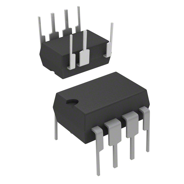
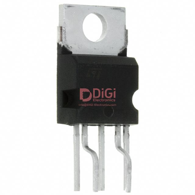
The VIPER100A-E integrates advanced power device technology with robust packaging options to address modern power conversion requirements. Offered in 5-Pentawatt and PowerSO-10 industry-standard configurations, it streamlines both through-hole and surface-mount assembly. These formats ensure broad compatibility across established PCB manufacturing processes, allowing direct substitution or migration between legacy and updated designs without PCB re-layout.
Compliance with JEDEC and EIA mechanical standards guarantees interchangeability and long-term supply chain stability, mitigating risks associated with component sourcing. The packages adopt ECOPACK® technology, meeting stringent RoHS directives. The lead-free material sets not only reduce hazardous substance content but also demonstrate a forward-compatible strategy for evolving global regulations. Experience in high-volume assembly lines confirms solder joint integrity and wettability in both wave and reflow soldering environments, minimizing failure rates associated with environmental legislation adaptations.
Automated and manual handling compatibility ensures that these devices suit diverse production scales, from rapid prototyping to large-scale industrial manufacturing. Marking practices, optimized for optical character recognition, contribute to error-free pick-and-place programming and downstream traceability. Lot codes and date information are encoded in accordance with major traceability standards, facilitating root-cause analysis during field returns or quality audits.
The packaging durability aligns with the demands of storage and shipment in various climates, and the antistatic features prevent ESD damage prior to board-level mounting. Integrating these specifications leads to significant reductions in both compliance-driven and operational risks, leveraging established infrastructure while preparing for future regulatory tightening. The combination of mechanical standardization and environmental accountability positions the VIPER100A-E as a robust choice for designers prioritizing lifecycle reliability and ecosystem compatibility.
Potential Equivalent/Replacement Models for VIPER100A-E
Selecting an equivalent or replacement for the VIPER100A-E requires a systematic approach grounded in both primary device attributes and secondary design constraints. The initial layer of comparison involves devices within the VIPer100 series, such as the VIPER100ASP-E. This series maintains a consistent platform, offering close alignment in terms of switching topology, protection features, power handling capability, and control schemes. However, individual models may exhibit nuanced variations in parameters such as startup current, switching frequency, or open-loop protection thresholds, which can manifest as subtle behavioral shifts in demanding designs.
A thorough examination of the detailed datasheets is indispensable, with particular attention to pin-for-pin compatibility, as mechanical drop-in replacement is often crucial for expedited field maintenance or cost-sensitive redesigns. It is essential to scrutinize thermal characteristics, including maximum junction temperature, package thermal resistance (RθJA, RθJC), and power dissipation limits, as these define the device’s operational reliability envelope under varied thermal loads. Even small deviations in package design or die attach technique may necessitate minor modifications in the PCB layout or system-level heat sinking. This step ensures that alternative parts not only meet electrical metrics but also sustain long-term performance under real-world operating conditions.
Looking beyond the immediate family, the broader VIPer series from STMicroelectronics introduces diverse variants with different integrated protection circuits, start-up times, and auxiliary functionalities like brown-out sensing or fault latching. Evaluating controllers with integrated high-voltage MOSFETs from alternative manufacturers also expands the available solution space. In such cross-ecosystem replacements, it becomes critical to verify conformance to core parameters: maximum drain-source voltage (Vds), continuous drain current, switching losses relevant to the specific PWM configuration, and interface logic levels compatible with associated drive circuits.
In practice, a common challenge lies in reconciling nominal datasheet values with real-world tolerances and worst-case design criteria. Tightly engineered SMPS solutions may exhibit sensitivity to propagation delays or slight changes in soft-start sequences between models, potentially impacting EMI signatures or transient response. Experienced practitioners often prototype candidate replacements and perform in-circuit validation, including thermal imaging and long-duration stress testing, to expose any edge-case instabilities. System topology, whether flyback, buck, or offline primary-side regulation, further shapes the parameter prioritization process, as loop compensation and transformer matching impose additional constraints.
A nuanced insight emerges when considering lifecycle support and platform robustness: devices with a stable supply chain, extended manufacturer support, and a track record of field reliability typically offset small specification premiums. Integrating such strategic considerations into the selection matrix reduces future risk, particularly for high-mix, low-volume production environments or designs targeting long service intervals.
Ultimately, an effective replacement strategy for VIPER100A-E centers on the interplay between electrical equivalence, mechanical interchangeability, and verified in-application stability. Prioritizing comprehensive validation steps and factoring in supportability ensures that substitution preserves both the technical integrity and long-term resilience of the finished system.
Conclusion
The STMicroelectronics VIPER100A-E exemplifies modern integration within offline flyback converter architectures by merging vital control, protection, and power switching components onto a single chip. At its core, the device leverages a high-voltage startup cell, PWM control, and comprehensive fault management circuitry, mitigating the necessity for discreet ICs and peripheral circuitry. This architectural consolidation directly translates to minimized component count, streamlined PCB layout, and a substantial reduction in both solution size and electromagnetic interference, all of which are essential criteria in high-density power electronics design.
The chip’s inherent protection suite—including overvoltage, overload, and thermal shutdown mechanisms—provides a robust operational envelope. These integrated safeguards not only promote long-term reliability but also simplify system qualification and compliance with international safety standards. Through current-mode PWM control, the VIPER100A-E maintains tightly regulated output across varying load conditions while achieving high conversion efficiency, a pivotal factor for meeting mandates such as EU ErP Lot 6 or ENERGY STAR. Effective compensation circuitry ensures stable operation over a broad input voltage range and diverse topologies, enabling the device to adapt readily to both universal AC inputs and application-specific requirements.
Practical deployment highlights the importance of precise board layout, especially at the primary-switching node, to optimize EMI performance and thermal dissipation. Adhering to recommended Kelvin-sensing and snubber network placement further refines noise immunity and extends device longevity under repetitive transient stress. With the monolithic design, typical layout iterations reveal reduced root-cause complexity when troubleshooting, expediting both R&D validation and transition to mass production. For procurement, the standardized and compatible device range supports supply-chain agility and design continuity, mitigating long-term obsolescence concerns.
A distinguishing insight emerges from the device’s adaptability across different power supply classes. The VIPER100A-E scales efficiently from auxiliary circuits in white goods to primary power sources in consumer and industrial end-equipment, without necessitating topology-specific redesign. Such flexibility underscores a migration path towards digital-ready platforms as system requirements evolve, allowing incremental upgrades within existing hardware envelopes. Its architectural focus on resilience and high efficiency demonstrates an optimum intersection of operational reliability, compliance readiness, and engineering practicality, positioning the VIPER100A-E as a cornerstone in offline power conversion design.