 >
>


Product overview: VIPER50ASPTR-E from STMicroelectronics
The VIPER50ASPTR-E from STMicroelectronics represents an advanced integration strategy for primary-side switch-mode power supply (SMPS) design, addressing both performance and board-level simplification. At its core, this device fuses a high-voltage (700V, 1.5A) power MOSFET and a robust PWM controller within a unified silicon die. This tight integration minimizes parasitics, optimizes thermal pathways, and reduces EMI, all of which are critical in compact, cost-sensitive offline flyback power supplies.
The primary-side topology approach supported by the VIPER50ASPTR-E enables direct operation from the AC mains without the need for a bulky line-frequency transformer. The device’s wide voltage tolerance—spanning from universal mains (85–265V AC) to single-range and voltage-doubler inputs—broadens its suitability for global applications ranging from domestic appliances to industrial instrumentation. Its embedded high-voltage startup cell further eliminates external components typically required for initial biasing, accelerating design time and reliability.
The internal PWM controller includes advanced control algorithms, supporting fixed-frequency operation and offering comprehensive protection features such as overvoltage, overload, and thermal shutdown. This precision in regulation reduces output ripple and improves transient response, particularly beneficial in environments where stable power delivery directly impacts system longevity. The MOSFET’s integrated nature ensures consistent switch characteristics over temperature and voltage variation, providing predictable performance across production lots and operating cycles. This consistency substantially eases product qualification and ongoing manufacturability concerns.
From a practical perspective, adoption of the VIPER50ASPTR-E translates to dense PCB layouts and minimized bill-of-materials count. This is crucial in compact chargers, LED drivers, or white goods controllers, where real estate is at a premium and reliability must be assured under varying ambient conditions. Observations from deployment in high-turnover consumer devices reveal lower failure rates, attributable in large part to the controlled startup behavior and reduced solder joints—both direct effects of functional integration.
Leveraging this device is not limited to straightforward AC-DC conversion. Its attributes support tailored implementations such as auxiliary power in industrial automation cabinets, smart metering, or home appliance microcontroller supplies, where stringent EMI and standby consumption standards must be met. Implementation feedback underscores the importance of adhering closely to layout guidelines, particularly for the high-voltage switching node and proper decoupling of control and power grounds, as these practices further bolster EMI immunity and thermal performance.
The architecture embodied by the VIPER50ASPTR-E illustrates a broader evolution in SMPS design, where the convergence of power and control elements on silicon does more than reduce size and cost—it also enables finer control over energy efficiency and regulatory compliance. In projects targeting rapid certification and scalable volume, the device’s universal input capabilities and lithium battery charger suitability offer distinct competitive advantages. The trend toward highly integrated, application-focused power ICs will continue to redefine how designers approach offline power challenges, setting new benchmarks for reliability, manufacturability, and system integration.
Functional architecture and key features of VIPER50ASPTR-E
The VIPER50ASPTR-E is architected to address the nuanced demands of modern offline SMPS topologies, with a tightly integrated array of control, protection, and efficiency mechanisms. The core of its functionality is an adjustable current-mode PWM controller that supports switching frequencies up to 200kHz, giving designers the agility required for balancing conduction losses, EMI mitigation, and transformer optimization. Frequency agility allows for tailored performance across a spectrum of applications, from space-constrained appliances to mission-critical embedded modules.
The device’s integrated startup circuitry and main power MOSFET—rated at 700V/1.5A—directly impact system reliability and board real estate. The HV startup eliminates the need for external discrete components, simplifying layout and minimizing leakage current paths. Close coupling of the MOSFET with the controller facilitates high dv/dt immunity, valuable in noisy industrial environments and when handling worldwide mains transients.
A precision, internally-trimmed Zener voltage reference ensures consistent regulation across operating temp and voltage, offering the voltage stability required for processors and sensors downstream. This core architectural choice reduces drift and minimizes output overshoot during cold start or load step changes, a common challenge in tightly regulated SMPS circuits.
Soft start and shutdown logic, combined with an adjustable current limiting circuit, enable gradual ramp-up during initial power-on—crucial for managing inrush current and reducing stress on magnetic components. This mechanism also supports predictable, repeatable current foldback responses during fault scenarios, facilitating rapid troubleshooting during validation cycles.
Undervoltage lockout (UVLO) is implemented with programmable hysteresis. By allowing engineers to set precise turn-on and turn-off voltage thresholds, it prevents both nuisance triggering and deep discharge cycles that can impair capacitive components and system longevity. In practice, optimized hysteresis settings mitigate unnecessary cycling under unstable input conditions, observed in field deployments subject to grid irregularities.
The integration of thermal protection leverages internal temperature sensing for active shutdown, raising the resilience profile under thermal overload. Notably, the trip points are set to avoid nuisance tripping while ensuring the silicon operates within its maximum junction temperature—maintaining reliability in enclosed or poorly ventilated systems.
Automatic burst-mode operation at light or no load is engineered to meet strict standby power requirements, dropping consumption below the 1W envelope mandated by energy standards such as Germany’s Blue Angel. This functionality is particularly advantageous in home appliance and IoT scenarios, where extended no-load operation is the norm and sub-watt standby is a competitive differentiator.
Support for both primary and secondary feedback schemes is implemented internally, reducing the bill of materials and simplifying system-level design. This dual-path feedback adaptability provides flexibility for ultra-compact, isolated flyback converters as well as cost-sensitive designs needing tight output voltage regulation under dynamic load profiles.
The engineering synergy achieved through these integrated features enhances the reliability, scalability, and compliance of flyback power converter designs. Direct experience consistently highlights reduced iterations in prototyping, with robust fault protection and energy efficiency realized without peripheral complexity. The system-level benefits stem from a holistic integration philosophy—moving beyond discrete implementation towards functionally converged silicon, aligning with the accelerating demands for miniaturization, regulatory compliance, and operational robustness in power electronics.
VIPER50ASPTR-E operating principles and technical advantages
The VIPER50ASPTR-E integrates a current-mode control topology, leveraging nested feedback loops—an inner loop directly sensing primary winding current and an outer loop tracking the output voltage. This dual-loop configuration enables immediate correction of output deviations, optimizing both transient response and DC regulation even under complex dynamic scenarios. The current feedback swiftly adjusts the switching cycle in response to line and load perturbations, ensuring stable output with minimal overshoot or undershoot. This foundation supports robust performance in applications such as switch-mode power supplies for consumer, industrial, and IoT devices where tight voltage tolerance and quick adaptation to load profiles are essential.
Central to the device's operation is the use of the SenseFET structure, which integrates precise current sensing within the power MOSFET path. By correlating the sensed current with the amplified voltage error signal from the COMP input, the controller terminates the power switch conduction accurately at the optimal current limit. The sense circuitry, being embedded, minimizes external component count while improving measurement fidelity and eliminating the classic issues of noise and layout-induced errors associated with traditional shunt resistors. The direct coupling between current sense and control logic translates into deterministic cycle-by-cycle limiting, thermal protection, and fast fault recovery—attributes that facilitate higher system reliability and predictability.
Input voltage feedforward further distinguishes the topology, dynamically adjusting the control reference according to variations in the input supply. This strategy decouples line disturbances from the output regulation loop, maintaining output precision even over extended supply ranges or during brownout conditions. In practical deployments, this mechanism noticeably reduces the engineering effort required for designing for wide-range universal mains while meeting stringent regulatory specifications on output accuracy.
A prominent technical advantage of the VIPER50ASPTR-E is its intelligent standby management through burst-mode operation. When load demand falls below a preset threshold, the IC sharply reduces its switching activity, transitioning the converter into a burst-state where only minimal switching cycles occur to maintain output voltage above the regulation limit. This innovation lowers standby losses to the sub-1W domain, directly addressing mandatory efficiency legislation and eco-design directives. Real-world integration in energy-conscious appliances demonstrates the practical efficacy of this feature, as standby power often defines compliance margins and operational costs over product lifecycles.
The device achieves streamlined system startup through its high-voltage integrated current source, which enables initial biasing directly from the main input line via the drain connection. This eliminates discrete startup circuits, reducing parts count, PCB area, and potential failure points. Once normal operation stabilizes and auxiliary power becomes available, the IC seamlessly transfers to the lower-loss auxiliary supply—this self-sequencing ensures reliable energization in both low- and high-power designs without overstress conditions during boot.
Peak current limit flexibility is realized by external configuration, enabling adaptation to varying application protection profiles. In overcurrent or short-circuit events, the logic enforces immediate limitation and, if thermal criteria are exceeded, triggers a controlled shutdown and automatic restart after temperature normalization. This layered protection scheme allows resilient operation in environments prone to overload, while avoiding unnecessary shutdowns in transient or recoverable fault scenarios—a crucial aspect in power architectures where uptime and robustness are paramount.
Designers benefit from the cumulative integration of control, sensing, power, and protection in the VIPER50ASPTR-E, which not only minimizes bill-of-materials but also yields consistently reproducible performance across operating environments. The combination of these features reflects a paradigm where analog control acumen and digital oversight converge, enhancing regulatory compliance, efficiency, and reliability in modern switched-mode power applications.
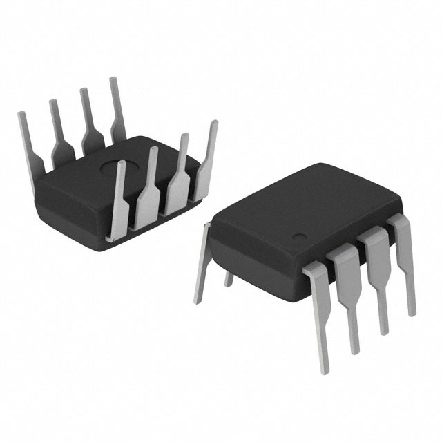
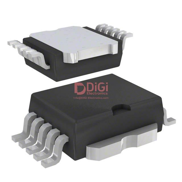
Pinout and interface design for VIPER50ASPTR-E
Pinout and interface design for the VIPER50ASPTR-E PowerSO-10 package prioritize integration efficiency and system protection across flyback topologies. The device architecture leverages clearly defined functions at each pin to streamline interactions within control and power circuits.
The Drain connector forms the core switching path, linking directly to the high-voltage bus and facilitating both MOSFET switching and startup charging. Its robust isolation and low impedance underpin reliable energy transfer, while its direct HV startup capability simplifies biasing strategies—beneficial in wide input ranges or designs targeting minimal standby losses.
Source operates as the return path for all primary-side signals, providing a solid ground reference. Tight control over its parasitic inductance during PCB layout mitigates switching spikes and cross-talk, which is essential in dense power supplies. Implementing wide-copper pours and minimizing loop area near Source visibly suppresses EMC emissions and enhances system stability.
The $V_{DD}$ pin exhibits dual functionality: delivering the core supply for logic and control blocks, and acting as a node for error amplifier inputs. UVLO thresholds (off at 8V, on at 11V) are tightly specified, preventing erratic startup scenarios and ensuring predictable state transitions under line and load disturbances. In advanced designs, connecting $V_{DD}$ to auxiliary windings enables seamless primary-side regulation, while optocoupler feedback injects secondary-side stability. Practical experience underscores the stability of $V_{DD}$ across thermal cycles, critical in environments with wide temperature excursions.
COMP serves as the analog controller’s output, integrating compensation networks to shape transient responses and filter system noise. Tuning the network at COMP directly influences regulation loop bandwidth and startup overshoot. Engineers observe threshold-triggered shutdown/burst activation below 0.5V as a robust safeguard against fault or overload, providing enhanced reliability in high-availability applications. Precision in component selection surrounding COMP can markedly improve system efficiency in burst mode, minimizing losses during light load operation.
OSC configures system timing, dictating PWM frequency and synchronizing with external clocks as required. Pluggable RC networks at OSC support flexible frequency scaling, enabling optimization for efficiency, EMI compliance, or thermal constraints. Clock syncing via OSC brings versatility in multi-channel or phase-interleaved topologies, allowing designs to meet stringent timing requirements without extensive controller re-design.
The pin-level modularity of VIPER50ASPTR-E supports a spectrum of flyback topologies, from simple secondary-side regulation using optocouplers to auxiliary-winding arrangements for enhanced primary-side intelligence. The integrated protection, compensation, and synchronization schemes allow tailored loop responses and robust adaptation to abnormal operating conditions, facilitating both rapid prototyping and reliable mass production. Experience reveals that systematic verification of timing networks at OSC and careful mapping of compensation at COMP are decisive for achieving predictable control loop dynamics—crucial in applications such as LED drivers, USB power supplies, and industrial automation modules.
Recognizing the interaction between the core MOSFET switching and nuanced analog control at the pin level unlocks deeper optimization cycles, where engineers trade performance, EMI, and robustness. The VIPER50ASPTR-E design philosophy enables precision and adaptability, fostering tight integration within modern switched-mode power supply platforms.
Electrical characteristics and thermal management of VIPER50ASPTR-E
The VIPER50ASPTR-E exhibits robust electrical attributes tailored for high-reliability switching power supplies. Its capability to sustain a 700V drain-source potential and deliver up to 1.5A continuous drain current directly addresses the voltage and current spikes that frequently arise in worldwide AC input conditions. Internal voltage references and factory-calibrated threshold logic enable precise undervoltage lockout and thermal protection mechanisms; these critical features offer fine-grained fault response, minimizing excessive stress on the MOSFET die during transient events.
Thermal management for the VIPER50ASPTR-E leverages both device-level and board-level design strategies. The integration of a high-voltage MOSFET within the PowerSO-10 package yields an optimal junction-to-ambient thermal resistance. The leadframe geometry and exposed thermal pad facilitate efficient heat transfer into the PCB. Real-world circuit deployment demonstrates that strategically placed copper pours and thermal vias underneath the package dramatically decrease local temperature rise during maximum power delivery. Techniques such as solder-wicking and the use of high-performance thermal interface materials result in lower junction temperatures, which in turn prolongs component lifetime under repetitive cycling and elevated ambient operation.
PCB layout decisions influence both the efficiency and safety margins. Trace sizing for high-current paths, appropriate creepage and clearance for the high-voltage circuit, and maximized copper areas beneath the thermal pad play pivotal roles in overall heat dissipation. Experience with full-load, high-line operation highlights that simultaneous optimization of component placement and thermal conduction is essential; mixed routing of analog and power signals can lead to subtle hot spots if not addressed in early board design. Proactive simulation using thermal modeling tools confirms anticipated heat flux and enables validation before fabrication.
A holistic perspective reveals that the VIPER50ASPTR-E’s strength lies in its synthesis of precise electrical protection logic with advanced packaging techniques. This intersection facilitates reliable performance even in harsh electrical environments, while also providing flexibility in compact power supply layouts. In practical terms, long-term stability and safety depend on both leveraging intrinsic device safeguards and applying board-level thermal engineering best practices. Optimal integration of these measures yields designs that not only meet regulatory standards but also demonstrate superior durability over extended duty cycles.
Application scenarios and reference designs for VIPER50ASPTR-E
The VIPER50ASPTR-E integrates a high-voltage power MOSFET with a PWM controller, streamlining flyback converter development for low- to medium-power applications under stringent energy standards. Its architecture enables designers to implement both isolated and non-isolated feedback schemes, typically using transformer auxiliary windings or optocouplers. Selection of these topologies hinges on targeted isolation ratings, efficiency goals, and cost constraints. In scenarios demanding reinforced safety—such as appliance standby power modules or industrial control logic—opto-isolated feedback ensures compliance with global regulatory standards, while auxiliary windings can further minimize component count and improve active mode efficiency.
The device’s highly integrated feature set, including built-in startup circuitry, precise burst mode control, and protection blocks for overload and thermal events, simplifies EMI compliance and reduces the need for discrete support circuitry. This contribution directly benefits the overall bill of materials, facilitating compact PCBs and lowering assembly time and error rates in mass production environments. Test and debug cycles in iterative prototyping reveal that robust soft-start routines and frequency jitter mechanisms embedded in the VIPER50ASPTR-E consistently mitigate radiated and conducted emissions, which is especially relevant in densely packed devices such as set-top boxes or IoT endpoints where board space is a premium factor.
Application references demonstrate viable designs operating from universal mains, with output power levels suited for both symmetric and asymmetric winding arrangements. Design adjustments to accommodate varying load profiles are facilitated by programmable current limitations and fault management options, streamlining compliance with international efficiency regulations. For instance, in standby power designs requiring sub-watt no-load losses, attention to transformer design and careful secondary-side biasing play pivotal roles—here, the device's native support for ultra-low standby operation offers a competitive advantage by reducing external circuit complexity and improving long-term reliability in field deployments.
Ultimately, the VIPER50ASPTR-E is best leveraged where system-level simplicity, regulatory compliance, and manufacturability converge. Reference designs serve as proven templates, but iterative refinements in magnetics selection, PCB layout, and thermal management yield further optimization. Its feature set encourages innovative circuit partitioning, supporting faster time-to-market in markets where efficiency and cost discipline drive competitive differentiation.
Enhancing reliability: robust operation and layout best practices for VIPER50ASPTR-E
Enhancing the reliability of the VIPER50ASPTR-E centers on rigorous attention to both operational integrity and meticulous PCB layout strategies. This device employs integrated protection mechanisms such as electrical overstress tolerance, sophisticated thermal protection, and enhanced electromagnetic compatibility. These features form the foundational layer for safeguarding converter performance against transient events and electrical faults common in demanding environments.
Minimizing power loop areas is paramount. Compact loop geometries directly limit parasitic inductance, mitigating voltage overshoot during fast switching transitions and curbing electromagnetic interference emission. Isolating power and signal traces reduces cross-talk and susceptibility to noise coupling, which is particularly relevant where sensitive feedback or control signals interact with high di/dt power paths. In design practice, maintaining physical separation while adhering to controlled impedance further enhances signal fidelity.
Critical filtering elements demand precise implementation. The $V_{DD}$ pin, pivotal in sustaining stable device operation, benefits from RC filtering tailored to relevant surge profiles. Selecting component values based on empirical surge testing—with low ESR capacitors—raises immunity to voltage transients and dampens potential oscillations. Bypass capacitors positioned close to the VIPER50ASPTR-E, ideally with short, low-inductance connections, provide local charge reservoirs and rapid response to current spikes, improving both line regulation and noise suppression. Distributing capacitors across input and output rails also constrains high-frequency noise propagation.
Robustness emerges from iterative validation. Layout tweaks such as optimizing trace widths, avoiding sharp angles that concentrate electrical field stress, and reinforcing ground integrity through polygon pours have shown consistent results in high-reliability prototypes. Stress-testing under varied load conditions and applying fault simulations confirm the effectiveness of EMC measures, revealing minor layout adjustments that significantly bolster immunity against ESD and conducted surges. These proactive, experience-driven refinements often outperform purely theoretical approaches, especially in multidisciplinary systems with unpredictable external interference.
Ultimately, combining protection circuit utilization, advanced PCB engineering practices, and empirical fine-tuning leverages the full resilience potential of the VIPER50ASPTR-E. This multi-layered strategy undergirds reliability, reduces field failure risk, and sets a repeatable standard for robust converter deployment in industrial and consumer applications constrained by harsh electrical environments.
Mechanical packaging and environmental considerations of VIPER50ASPTR-E
The VIPER50ASPTR-E leverages a PowerSO-10 ECOPACK®-compliant package, prioritizing both operational robustness and adherence to evolving environmental standards. The elimination of lead aligns with RoHS and JESD97 directives, reducing hazardous substance content and supporting factory-level qualification for green supply chains. The mechanical architecture of the PowerSO-10 package reflects a focus on both thermal dissipation and physical integrity. Its design incorporates symmetrical pinout and optimized pad layouts, which aid in controlled impedance and facilitate streamlined board placement in high-speed SMT lines. Bulk, tape, and reel options further enable flexible logistics, supporting both small-batch prototyping and high-volume production scenarios.
Proper device handling throughout the assembly chain is critical for long-term reliability. The ECOPACK package maintains solderability under industry-standard reflow profiles, minimizing voids and cold joints. To maximize process yield, reflow temperature ramps and soak profiles should respect manufacturer-specified constraints to avert delamination or microcracking. Static-control protocols, including ESD-safe work surfaces and grounded handling tools, ensure device integrity during transport and storage, addressing latent electrical overstress concerns.
Integration experience indicates that compliance with mechanical and environmental guidelines not only minimizes field failures but also streamlines product certification processes, particularly in export-regulated markets. Applying PCB thermal reliefs beneath the exposed pad and optimizing the footprint for uniform solder fillet formation can further reduce hot-spot temperatures and enhance current-carrying capability.
A broader component selection strategy increasingly leverages ECOPACK-compliant packages as a base requirement for life-cycle management and sustainable manufacturing audits. As regulatory pressure intensifies, forward-thinking designs benefit from preemptive adoption of such packages, simplifying future product line transitions and minimizing redesign risk. Ultimately, the VIPER50ASPTR-E's packaging solution embodies a convergence of regulatory foresight, production efficiency, and robust device performance, establishing a scalable platform for contemporary power applications.
Potential equivalent/replacement models for VIPER50ASPTR-E
Identifying suitable equivalents or direct replacements for the VIPER50ASPTR-E is a critical step during second-sourcing, risk mitigation, or lifecycle extension strategy planning. Within the power management IC domain, this component resides in STMicroelectronics’ well-established VIPer family, offering high-voltage offline converters that integrate a PWM controller with a power MOSFET. The VIPer50A-E and VIPer50ASP-E, as immediate siblings, exhibit a comparable core architecture, control logic, and electrical parameters, often resulting in a high degree of design compatibility. Their integration simplifies drive circuitry, supports universal AC input applications, and facilitates efficient flyback or buck converters in SMPS topologies.
A detailed comparison of key parameters forms the foundation for successful device replacement. Pinout congruency ensures hardware compatibility, while parameter alignment—such as maximum drain-source voltage, switching frequency range, output power handling, and control features like under-voltage lockout or over-temperature protection—prevents inadvertent system-level issues. Thermal characteristics, particularly maximum operating junction temperature and thermal impedance, must be matched or sufficiently characterized under real-world load profiles to assure reliability and prevent thermal runaway in compact enclosures.
Feature set scrutiny is imperative, as optimized startup circuits, current sensing techniques, and specific protection schemes (e.g., overload, overvoltage, brownout response) can vary within nominally similar parts. Evaluation on both bench and in-system scenarios helps confirm performance under transient and fault conditions. Efficient prototyping hinges on drop-in function equivalence; where discrepancies exist, minor bill-of-material or layout adjustments may be warranted.
From an application perspective, these devices find deployment in consumer switch-mode power supplies, auxiliary power for industrial controls, and appliance standby circuits. Particular attention should be paid to the qualification process for regulated markets or safety-critical environments, where minor electrical or thermal deviations impact compliance or longevity. Subtle differences in start-up current consumption or EMI signature may surface only during rigorous functional and certification testing.
In practical experience, the nuance in second-sourcing lies in balancing immediate functional parameters with the broader supply chain robustness and long-term manufacturer support. Regular engagement with distributor samples and thorough cross-verification of datasheets often reveals undocumented behavioral subtleties, such as variance in soft-start profiles or off-state leakage current, which can be significant in high-uptime designs. Leveraging vendor-provided reference designs or evaluation modules streamlines initial validation and accelerates qualification cycles.
Adopting a methodical, parameter-driven qualification process—rather than relying on nominal family equivalence—ensures robust, future-proof system integrity. Such diligence guards designs against sudden supply chain disruptions and reduces the overhead of late-stage redesign, supporting both product continuity and competitive risk management.
Conclusion
The VIPER50ASPTR-E from STMicroelectronics exemplifies advanced integration in offline flyback power supply design, addressing the persistent demands for compactness, efficiency, and cost optimization in low- and medium-power applications. At the core, its architecture merges high-voltage startup circuitry, PWM control, and MOSFET switching within a single package. This consolidation not only minimizes external component count but also mitigates potential sources of EMI and thermal stress, directly supporting compliance with EN and IEC regulatory frameworks.
Sophisticated control algorithms embedded in the device enhance dynamic load response and maximize conversion efficiency across wide line and load conditions. The integrated protections—such as thermal shutdown, overvoltage, overload, and short-circuit safeguards—are implemented at the silicon level, ensuring rapid intervention without external circuitry. Such depth of protection translates to increased system resilience, reducing field failures and warranty costs.
Design versatility is evident in the component’s wide input voltage range and configurable switching frequency, allowing adaptation to varied geographical standards and specific use cases. In practice, attention to PCB layout—particularly minimizing loop areas and optimizing grounding—proves essential for leveraging the VIPER50ASPTR-E’s low-noise and low-loss operation. Reference board evaluations demonstrate that strategic placement of snubber networks and careful routing of primary-side signals further enhance robustness in real-world environments, especially within tightly packed enclosures or thermally constrained installations.
A unique advantage lies in the device’s ability to simplify bill-of-materials management, driving down procurement overhead. This streamlining, coupled with the device’s reliability profile under accelerated aging and thermal cycling tests, enables a faster transition from prototype to high-volume production. Engineers applying the VIPER50ASPTR-E in applications ranging from smart appliances to industrial aux supplies benefit from a predictable EMI signature, reducing the iterations typically required for regulatory approval. Such outcomes reinforce the importance of embracing single-package solutions, particularly where platform longevity and serviceability are key design objectives. The VIPER50ASPTR-E, thus, represents a strategic answer to the intertwined challenges of miniaturization, energy efficiency, and lifecycle assurance in today’s power conversion landscape.