


 >
>


Product overview of VIPER22ASTR-E
The VIPER22ASTR-E from STMicroelectronics represents an integrated approach to offline switch-mode power supply design, combining a high-voltage power MOSFET and a current-mode PWM controller within a unified silicon architecture. This monolithic integration effectively reduces propagation delays and optimizes dynamic response, facilitating reliable startup and stable operation across variable line and load conditions. Leveraging ST’s proprietary silicon process, the device exhibits consistent performance over a broad temperature range, ensuring robust functionality in environments subject to wide fluctuation.
At the core, the current-mode PWM controller enables cycle-by-cycle primary-side current limitation with inherent secondary-side regulation accuracy. This topology enhances transient response, mitigates overshoot, and provides superior noise immunity under load perturbations. Control algorithms are integrated to prevent overvoltage and undercurrent conditions, contributing to a greater margin against output faults. Practical deployment reveals that the internal high-voltage MOSFET retains low RDS(on) characteristics, supporting efficient switching and minimizing conduction losses during prolonged operation. These features collectively result in improved energy efficiency, especially beneficial where applications must comply with stringent standby power consumption standards.
The compact 8-SOIC package offers mechanical robustness alongside streamlined PCB layout options. High-voltage isolation, reduced external component dependencies, and intrinsic protections such as thermal shutdown, overcurrent, and short-circuit sensing lead to significant design simplification and reliability. This integration is particularly advantageous when configuring auxiliary power rails for microcontroller-based motor control drives, as it eliminates the need for bulky discrete switching elements and external sense resistors.
In application contexts such as battery chargers, standby circuitry for consumer electronics, and industrial auxiliary supplies, the VIPER22ASTR-E’s fixed-frequency operation supports rapid load regulation and mitigates EMI emissions through controlled edge rates. Insights from practical implementation highlight that careful PCB layout—optimizing ground returns and minimizing loop areas—amplifies the performance benefits of the single-chip approach. Additionally, designers exploit the flexibility of built-in protections to streamline compliance with international safety and efficiency standards, reducing qualification overhead and time-to-market.
Integrating core circuit functions in a silicon platform, this device embodies a decisive evolution towards modular and scalable SMPS solutions. The reduction of external component count not only lowers BOM costs but also minimizes avenues for field failure, reinforcing product longevity in mission-critical installations. Evaluation reveals that leveraging the VIPER22ASTR-E accelerates design cycles by enabling predictable startup and shutdown sequences and simplifying thermal management considerations, thus allowing engineers to focus on system-level optimizations rather than discrete power stage troubleshooting.
Key features of VIPER22ASTR-E
The VIPER22ASTR-E embeds a suite of features that address demanding requirements in modern switch-mode power supply (SMPS) architectures. At its foundation, the device utilizes a fixed 60 kHz switching frequency, facilitating predictable timing for EMI filter design and enabling high efficiency while minimizing conducted and radiated electromagnetic interference. The frequency selection balances transformer core loss against switching losses, a critical optimization in efficient flyback and buck converters targeting both cost-sensitive and performance-driven applications.
Operating flexibility is maintained through a broad VDD range of 9 V to 38 V. This wide span accommodates various auxiliary supply configurations and fortifies circuit stability against line-side voltage fluctuations. Such tolerance is particularly beneficial in global platforms and systems exposed to erratic mains, where undervoltage scenarios would traditionally challenge reliable start-up and steady-state performance.
Current mode control is pivotal within the device’s architecture. By sampling the transformer’s primary side current, the controller achieves tight output voltage regulation and rapid transient response. This control topology inherently mitigates subharmonic oscillations and simplifies loop compensation, streamlining development and shortening design cycles for dense or highly integrated SMPS modules. In practice, fast and precise output regulation proves essential in consumer electronics and industrial controls, where load profiles vary abruptly and output accuracy must be maintained without complex external feedback networks.
The integrated auxiliary undervoltage lockout (UVLO) with hysteresis enhances operational safety. This mechanism disables switching below a certain voltage threshold and only re-enables when a higher recovery voltage is achieved, preventing erroneous oscillation during brown-out or supply ripple events. Engineering teams routinely observe that such robust UVLO architectures reduce maintenance cycles and field failures, especially within geographically distributed installations or harsh industrial deployments.
Rapid converter initialization is driven by the internal high-voltage start-up current source. This feature eliminates the need for large external start-up resistors, reducing standby losses and accelerating system boot-up. Devices leveraging this architecture often exhibit cold-start times under 150 ms, supporting applications like smart meters and automotive electronics where immediate power delivery upon energization is a requirement.
Reliability is reinforced through a comprehensive suite of integrated protections, including thermal shutdown, cycle-by-cycle overcurrent protection, and overvoltage intervention via HICCUP mode. The automatic restart capability allows systems to self-recover after transient faults, a design advantage in mission-critical power supplies where uptime and minimal intervention are imperative. In differentiated builds, designers have exploited these mechanisms to endure repeated stress events, such as lightning surges or load-induced faults, significantly extending hardware lifespans.
From an engineering perspective, the VIPER22ASTR-E’s architecture supports a philosophy of self-contained resilience and adaptive flexibility. These characteristics position it as an optimal choice in power converter designs that demand robust tolerance to input and environmental variability, comprehensive fault coverage, and simplified system-level integration without excessive external component overhead. The sum of these features shortens design cycles while elevating reliability standards, meeting the escalating requirements of contemporary power electronics.
Electrical and thermal characteristics of VIPER22ASTR-E
Electrical and thermal performance of the VIPER22ASTR-E is governed by tightly specified parameters that define safe operational boundaries. The architecture utilizes a high-voltage start-up cell, current-mode PWM controller, and integrated power MOSFET, all calibrated for robust switching applications. Absolute maximum ratings—spanning drain-source voltage, supply voltage, and junction temperature—serve as hard constraints that protect device integrity against transient surges and abnormal events. However, steady-state reliability arises from consistent operation well below these thresholds, leveraging detailed electrical limits such as VDD undervoltage lockout and drain current clamping to prevent thermal runaway or latch-up phenomena during both start-up and fault conditions.
Device characterization at a junction temperature of 25°C and VDD of 18 V establishes baseline electrical behavior. Parameters such as turn-on/turn-off thresholds, oscillator frequency uniformity, and dynamic load response are validated under these controlled conditions, facilitating predictable circuit design. The clear demarcation of logic thresholds, soft-start currents, and over-temperature/shutdown levels provides engineers with actionable data for specifying feedback networks, protection circuits, and EMI filters. Current sense accuracy and propagation delays are critical for applications requiring precise overload detection and rapid switching, and VIPER22ASTR-E’s parameter set reflects a balance between speed, noise immunity, and energy efficiency.
Thermal characteristics are directly influenced by implementation choices at the PCB level. Standard benchmarks using a single-sided FR4 PCB with 200 mm² copper (35 μm thick) provide thermal reference points, such as junction-to-ambient resistance, crucial for predicting steady-state temperature rise. Heat dissipation pathways are primarily through the copper spread and the thermal pad, making layout optimizations a high-leverage means of improving device lifespan in high-cycle or continuous-duty environments. Thermal simulation at the design stage, in tandem with empirical measurements using thermocouples at hotspots, can reveal unforeseen thermal bottlenecks introduced by component density or inadequate airflow.
In practical deployment, subtle deviations from datasheet mounting scenarios—such as reduced copper area or increased ambient temperature—demonstrate the necessity for derating margins and auxiliary cooling measures in fielded designs. Actual stress profiles, including dynamic load cycles and surge events, reinforce the utility of integrating conservative design allowances and periodic real-time monitoring for critical applications. Experience shows that consistent attention to board layout symmetry, trace width for current return paths, and spacing from heat-generating elements such as power diodes, materially improves thermal uniformity and long-term electrical performance.
A layered approach to leveraging VIPER22ASTR-E’s strengths begins with respecting foundational electrical and thermal constraints, complementing them with predictive analysis and validation under real system conditions. This methodology not only preserves device reliability but also enhances overall power supply robustness and efficiency, especially in low-standby, isolated offline converter topologies. The interplay between electrical thresholds, thermal paths, and feedback responsiveness forms the core of optimized SMPS design, and a nuanced grasp of these relationships enables the realization of resilient, compact, and energy-conscious systems.
Functional operation principles of VIPER22ASTR-E
The operational architecture of the VIPER22ASTR-E is anchored in a current mode control framework, whereby the device achieves rapid, accurate output regulation and high immunity to fluctuations across dynamic loading conditions. This approach directly influences loop bandwidth and transient response, facilitating low output ripple and robust regulation. Tight feedback is established by processing the current sense signal rather than solely relying on output voltage, integrating response time improvements and enabling inherent short-circuit protection. The internal sense resistor and high-speed comparator chain act as the primary determinants of ON/OFF transitions for the embedded power MOSFET, minimizing propagation delays and reducing susceptibility to noise—a practical advantage in applications such as precision battery chargers or auxiliary switched-mode supplies.
Extensive flexibility is conferred through the device’s wide VDD range, supporting both primary-supply and auxiliary-winding biasing methods. In systems where an auxiliary winding is employed for VDD supply, the requirement for large-value start-up capacitors lessens substantially. This design reduces overall board real estate and system cost while yielding faster power-up sequences. For time-sensitive applications such as PLC modules or smart IoT nodes, this feature prevents lengthy delays during initialization and streamlines user experience in rapid-cycling environments.
Regulation strategy in battery charger implementations leverages the device’s adaptability to a dual feedback loop, using an optocoupler and a dedicated shunt regulator like the TSM101 dual op-amp. In this topology, simultaneous voltage and current sensing facilitate the realization of either precise constant voltage control or constant current limiting modes. Adjustments in the feedback network allow compliance with a variety of battery chemistries or load characteristics, without fundamental changes to the switching core. This modularity supports both rectangular (constant) and tapered charging profiles, enhancing versatility for designers targeting multi-battery platforms.
The feedback (FB) pin’s direct coupling to the current sense loop, bypassing voltage-centric detection, distinguishes the device’s control accuracy. Any instantaneous changes in load current evoke a proportional response in the switching action, enforcing precise cycle-by-cycle energy delivery. The fast internal comparator logic enforces a deterministic switching threshold, supporting stable operation under highly dynamic line or load variations—a hallmark in power systems required to meet stringent EMC and safety standards.
Low-load and burst-mode management is realized through intelligent cycle skipping. Under minimal load scenarios, the controller automatically enters a burst-mode regime, selectively suspending switching operations to minimize core and gate-drive losses. This mechanism ensures high light-load efficiency, particularly critical in always-on standby supplies or zero-watt designs demanded by contemporary eco-standards. Oscilloscope traces confirm significant reductions in VIN-to-output power dissipation during standby, directly benefiting thermal design margins and system energy certificates.
The start-up mechanism involves an integrated high-voltage current source derived directly from the input line. Upon initial energization, this source charges the VDD capacitor just sufficiently to enable controller logic, eliminating the need for bulky and slow-charging external components. After start-up, the internal circuitry seamlessly transitions to MOSFET gate control governed by the feedback loop, ensuring a controlled ramp without overshoot or instability. This architectural trait improves system resilience during brown-in events or under-spec input ramp scenarios, as seen in industrial automation nodes and compact wall adapters.
A notable aspect emerges from the device’s ability to combine integration and control. By condensing gate-drive, high-voltage startup, and current mode logic onto a monolithic silicon platform, the VIPER22ASTR-E reduces external part count, enhances MTBF, and simplifies layout—outcomes that directly translate into cost-effective, reliable power designs for space and efficiency constrained systems. The fusion of these functional blocks demonstrates a synergistic path towards smarter, smaller, and more robust off-line power solutions.
Protection mechanisms in VIPER22ASTR-E
The VIPER22ASTR-E integrates a comprehensive suite of protection mechanisms designed to elevate both device reliability and operational continuity. At the core, overtemperature protection functions through real-time thermal monitoring embedded at the silicon level. When internal temperatures breach the designated safety threshold, a shutdown sequence is engaged, halting switching activity to prevent thermal runaway and subsequent damage to peripheral circuitry. This action is not static; the system continuously reassesses thermal conditions, permitting automatic re-enablement once the die temperature normalizes, thereby supporting designs that demand resilient thermal cycling under variable loads.
Overcurrent protection is orchestrated via precise drain current sense circuitry tightly coupled to the controller logic. When current exceeds predefined boundaries, the controller limits output conduction cycles, clamping current flow to safeguard downstream components such as rectifiers and magnetic elements. This dynamic current regulation acts as a preventive barrier against short-circuit scenarios and inadvertently high load conditions, ensuring device integrity and extending mean time between failure (MTBF) for power rail subsystems.
The overvoltage protection architecture protects the VDD pin by monitoring supply rail excursions above the safe operating area. Upon detection of excessive VDD, a reset-and-restart protocol is triggered, which rapidly disables power delivery and restarts the controller after a short cooling-off interval. This cyclical intervention shields both the device core and connected payloads from overstress events commonly induced by transient surges or feedback loop instabilities. System-level experience confirms that such robust VDD management significantly reduces the risk of latch-up and catastrophic breakdown in automotive and embedded industrial designs.
A distinctive operational feature is the auto-restart—HICCUP mode—which underpins the device’s fault recovery strategy. When any protection mechanism activates, the controller suspends switching, evaluates fault clearance, and then automatically restores normal output after a short hold-off. This self-healing loop not only minimizes downtime but also avoids repeated manual resets, aligning with strict uptime and compliance requirements in mission-critical sectors like medical instrumentation or network infrastructure. Notably, the seamless integration of these layers fosters a synergistic effect where transient faults rarely propagate to system-level failures.
This layered approach reflects a design philosophy favoring proactive fault containment and rapid system restore, which is essential in environments where power supply availability underpins core functionalities. Practical deployment confirms reduced field returns and increased customer confidence, especially when exposed to complex, unpredictable load profiles. These mechanisms collectively define the VIPER22ASTR-E's reliability fingerprint, providing engineers with a robust platform for both high-volume consumer applications and demanding industrial use cases.
Pin configuration and application considerations for VIPER22ASTR-E
Pin configuration for the VIPER22ASTR-E in its 8-SOIC package is engineered for streamlined implementation within typical switched-mode power supply (SMPS) topologies. The device segregates high-voltage switching (Drain), ground reference (Source), primary bias (VDD), and control loop (Feedback), enabling a clean functional partition across the PCB. Routing for the high-voltage drain pin should be prioritized for both creepage clearance and current-handling capability, reducing radiated and conducted EMI. Simultaneously, feedback and VDD pins must be shielded with ground planes or signal referencing techniques to prevent noise injection that could degrade control accuracy.
While the package appears compact, the interaction between pin allocation and peripheral circuit design is often critical for both electrical and thermal performance. Isolating the high-energy switching node from low-level signal paths mitigates common-mode noise propagation. Trace geometry, layer stackup, and decoupling strategies directly affect how susceptible the feedback path becomes to spurious transients. For example, routing the feedback line away from drain and source traces, backed by local RC damping at the entry point, actively suppresses high-frequency pickup.
In power supply designs such as USB chargers, feedback regulation typically utilizes an optocoupler to bridge primary and secondary sides. The optocoupler load resistor and associated compensation network, connected to the feedback pin, should be dimensioned not only for static regulation but also for dynamic response—tight coupling can enhance line/load adjustment at the cost of increased loop sensitivity. Performance trade-offs arise when balancing loop speed, noise immunity, and component tolerances. For critical edge-case loads, employing precision shunt references and low-leakage optocouplers noticeably sharpens regulation and minimizes drift.
Auxiliary circuitry selection, specifically the sizing and ESR of VDD bypass capacitors, shapes start-up current availability and regulation stability. Underestimating the thermal implications of repeated start-stop cycles may lead to temperature-induced bistability or delayed protection triggering. Adopting film or ceramic bypass capacitors, with close proximity to the VDD pin, usually delivers lower impedance across the operating frequency spectrum, supporting clean auxiliary supply rails and minimizing inrush events. Power and ground return paths must be defined to guide switching currents away from analog ground nodes, reducing the likelihood of controller latch-up.
Application success with VIPER22ASTR-E pivots on disciplined interconnection between silicon and PCB layout. Manufacturing tolerances in pad placement or solder mask registration cannot substitute for deliberate layout strategies; early-stage simulations—especially parasitic extraction and EMC validation—yield outsized dividends by exposing issues before fabrication. In environments where compactness competes with thermal dissipation, copper pour management and via stitching adjacent to the source pad efficiently spreads current and aids convection, maintaining device reliability over the appliance lifetime.
By integrating these design insights and layout optimization practices, SMPS implementations using the VIPER22ASTR-E reliably achieve high conversion efficiency, low emissions, and robust operational margins, even under harsh line conditions or fast transient loads. Practical refinement of feedback, power handling, and auxiliary support directly translates to enhanced regulation and longevity, establishing the device as a versatile and dependable platform component for modern power conversion architectures.
Package information for VIPER22ASTR-E
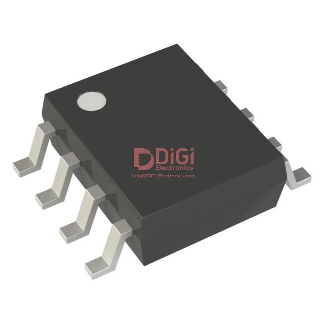
The VIPER22ASTR-E integrates a robust feature set within an industry-standard 8-pin SOIC (Small Outline Integrated Circuit) package, which addresses stringent demands in offline switch-mode power supplies. The package design balances minimal footprint with compliance to creepage and clearance requirements, essential for safe operation in high-voltage mains-powered environments. This careful package engineering mitigates risks related to surface arcing and insulation breakdown, crucial for regulatory conformity and long-term application uptime.
SOIC-8 package compatibility with standard pick-and-place machines and reflow soldering lines streamlines manufacturing in high-throughput environments. The ECOPACK® grade option underscores a growing commitment to environmentally sustainable electronics, aligning with evolving supply chain and compliance landscapes. During system hardware development, referencing the detailed mechanical and thermal specification is fundamental. Board designers often optimize copper area around the device, leveraging the package’s exposed pad and pin layout to maintain junction temperature margins during peak load or adverse ambient conditions. This is vital for applications in confined enclosures or thermally challenging installations, where reliance on ambient cooling alone may prove insufficient.
The family’s pinout uniformity allows for straightforward design migration to alternative package variants, such as DIP-8 or slimline SOIC, facilitating rapid prototyping and production scaling with minimal redesign. Cross-compatibility in the VIPer22A series is particularly advantageous for platforms targeting both leaded and SMT assembly, or where cost-down exercises dictate package substitution strategies.
Field experience highlights the importance of revisiting PCB creepage, especially in primary-to-secondary transitions, with solder mask and silkscreen clearance practices factored in during the layout phase. Employing wide copper pours under the SOIC-8 can significantly enhance thermal dissipation without compromising electrical isolation. Device reliability is closely tied to such nuanced layout practices, particularly in universal input (85–265 VAC) topologies where voltage stress and load-cycling accelerate aging mechanisms.
The choice of SOIC-8 for the VIPER22ASTR-E is a direct response to the competing requirements of space-saving, automated manufacturability, safety, thermal performance, and regulatory drivers. Optimization at both the device and board levels yields scalable and durable power conversion solutions for deployments ranging from consumer adapters to auxiliary supplies in industrial controllers. The subtle synergy between package engineering and power design practices forms the foundation for high-efficiency, long-service-life power electronics built on the VIPER22A platform.
Potential equivalent/replacement models for VIPER22ASTR-E
Evaluating suitable substitutes for the VIPER22ASTR-E demands a methodical approach, centering on electrical, mechanical, and reliability attributes. Within STMicroelectronics’ catalog, the VIPer22ADIP-E and VIPer22AS-E emerge as direct alternatives, retaining identical internal architecture and performance envelope. These devices differ primarily in packaging, ensuring pin-to-pin compatibility and streamlining integration into existing layouts without necessitating PCB revisions. This minimizes design disruption and facilitates rapid transition in procurement-sensitive environments.
Expanding beyond native package variants introduces broader consideration of switch-mode power supply ICs featuring an integrated power MOSFET and current-mode control. Such alternatives must offer comparable wide-range input voltage operation, switching frequency flexibility, and integrated protective mechanisms, notably overvoltage, overload, and thermal shutdown functionalities. Parameters including startup and operating VDD requirements, drain-source voltage capabilities, peak current limits, and enable/disable features must be meticulously aligned with application constraints. Selection should further account for available documentation and reference designs, supporting both regulatory compliance and fast time-to-market cycles.
Pinout verification is a non-negotiable step, especially when transitioning between manufacturers or package styles. Discrepancies may result in system-level incompatibility, leading to failures in EMC, surge, or insulation testing phases. Thermal characteristics warrant extra scrutiny; subtle differences in Rth(j-a) impact heat dissipation strategies, dictating board layout adjustments or heatsink sizing. Certification continuity, especially for safety and EMI standards, hinges on maintaining equivalency in maximum ratings and fault response behavior.
Practical implementation reveals that secondary-side feedback loop matching is often overlooked when replacing controller ICs, potentially degrading transient response or output stability. Direct substitutions have demonstrated success when isolation transformer parameters and snubber networks remain within original design tolerances. Iterative prototyping and pre-compliance screening accelerate validation and mitigate downstream risks, establishing the importance of a structured evaluation protocol.
A nuanced approach advocates for a dual-path assessment: prioritize drop-in replacements for speed, but simultaneously cultivate a shortlist of alternative switcher ICs with robust supplier footprints and multi-source availability. Strategic diversification not only hedges supply risk but enhances design resilience and scalability.
Conclusion
The VIPER22ASTR-E from STMicroelectronics represents an advanced semiconductor solution optimized for low-power offline switch-mode power supply (SMPS) applications. At its core, the device integrates a high-voltage start-up circuit, PWM controller, and protection subsystems into a compact, single-package design, minimizing the external component count. This integration directly addresses board space constraints common in consumer and industrial designs, streamlining PCB layouts while simplifying input filtering and EMI management thanks to the inherent current mode control topology.
Current mode control in the VIPER22ASTR-E yields fast transient response and inherent cycle-by-cycle current limitation. This architecture ensures reliable operation under step load conditions often encountered in appliances and auxiliary supplies. The wide input voltage range, typically operating from 85 to 265 VAC, supports global deployment without redesign, accommodating grid variations and improving product flexibility. The flexible package options—including industry-standard DIP and SMD forms—facilitate straightforward integration into both existing and new platforms, offering versatility within procurement logistics and assembly lines.
The device’s comprehensive protection mechanisms—including under-voltage lockout, overload, and thermal shutdown—contribute to system resilience. These features reduce field failures caused by anomalous grid conditions or component stress, translating to higher end-application MTBF and reduced warranty claims. In actual deployment, such robustness allows for aggressive design-to-cost optimization without sacrificing operational reliability—especially valuable in price-sensitive markets.
VIPER22ASTR-E’s inclusion in the VIPer22A-E family enables platform scalability. Pin-to-pin compatibility and consistent electrical characteristics empower engineers to implement power level adjustments or perform drop-in substitutions with minimal qualification overhead. In production ramp-up scenarios, this compatibility streamlines multi-sourcing strategies and inventory management, ultimately reducing supply chain risk.
Selecting VIPER22ASTR-E demonstrates the benefits of leveraging highly integrated power ICs in modern SMPS designs. The device’s balance of functional density, flexibility, and cost efficiency aligns well with market drivers prioritizing compactness, energy savings, and global operability. Applications such as appliance controllers, metering, and auxiliary standby supplies benefit from this approach, achieving both engineering and business performance objectives through smart component choices.


