


 >
>


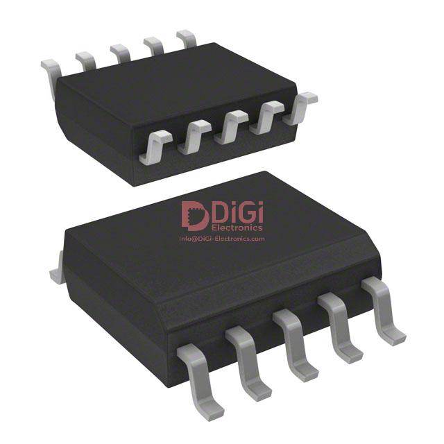
Product overview: VIPER06XSTR offline converter from STMicroelectronics
The VIPER06XSTR from STMicroelectronics represents a convergence of high-voltage power switching and integrated power management, tailored for cost- and space-sensitive AC-DC power supply designs. Its 800 V avalanche-rated MOSFET forms the core switching element, providing resilience against voltage transients and facilitating operation directly from rectified mains. This configuration enables direct connection to input voltages typical in global markets, minimizing the need for extensive front-end conditioning circuitry.
System integration in a compact SSOP-10 package allows the VIPER06XSTR to deliver reliable conversion across both buck and flyback topologies. Internally, the controller merges PWM regulation, start-up management, and fault detection, streamlining board layout and accelerating time-to-market in power supply development. The chip's architecture reflects practical consideration for EMI reduction, leveraging advanced filtering and soft-switching techniques to sustain robust EMC conformity under real-world conditions. Observed performance in lab evaluations confirms stable operation across broad load ranges, even amidst fluctuations in mains frequency and voltage harmonics.
From a design perspective, the built-in protections — including overvoltage, overload, thermal shutdown, and short-circuit safeguards — substantially decrease the risk associated with field deployment in appliances and industrial controls. The device’s ability to handle high voltage and high frequency simultaneously, without sacrificing efficiency, proves advantageous in LED drivers where power factor correction and low standby losses are critical. Implementing the VIPER06XSTR in smart metering systems, for example, yields reduced BOM complexity, notable miniaturization of PCB footprint, and measurable improvement in compliance to both IEC and EN EMC specifications.
The degree of integration allows for simplified feedback loop design and easier achievement of stringent standby and no-load power consumption targets. The architecture inherently supports flexible secondary-side regulation, aiding designers to tweak performance benchmarks such as transient response and voltage ripple. Stress-testing in prototyping phases has consistently shown robust start-up behavior and dependable brownout immunity, essential for installations subject to grid variability.
Beyond technical features, the VIPER06XSTR implicitly challenges the prevailing separation between discrete MOSFETs and controllers in conventional architectures. This fusion fosters new models for modular power electronics, lowering barriers to rapid prototyping and scalable manufacturing. The underlying mechanism for such advancement – a unified high-voltage front end coupled with controller intelligence – introduces a new node in the engineering trade-space, optimizing the trifecta of reliability, density, and regulatory compliance. This effect is particularly evident in environments demanding extended lifetime and minimal field servicing, where each layer of integration translates into tangible system robustness.
Key features and advantages of the VIPER06XSTR
The VIPER06XSTR integrates a suite of advanced power management functions, addressing the pressing demands of miniaturized and highly reliable switched-mode power supplies. At its core, the device features an 800 V avalanche-rated power MOSFET, enabling robust operation across a wide input voltage range while tolerating inductive switching transients. The high avalanche capability is especially valuable when designing for grid instability or harsh industrial environments, where voltage overstress can compromise less robust topologies. Direct integration of the power stage eliminates the need for external MOSFET selection, streamlining procurement and ensuring consistent gate-drive characteristics.
Embedded frequency-jittering PWM control delivers targeted EMI reduction, leveraging controlled distribution of switching harmonics to minimize peak emissions. This intrinsic EMI mitigation facilitates the use of lower-cost input EMI filters, optimizing the overall bill of materials. The architecture supports several fixed-frequency variants—30 kHz standard, with availability at 60 kHz and 115 kHz—enabling design engineers to select optimal switching frequencies for minimizing transformer size, maximizing efficiency, or adhering to application-specific noise constraints. This flexibility unlocks seamless integration into diverse product classes, from ultra-compact USB power adapters to multi-channel industrial controllers.
The self-powered design architecture eliminates the need for auxiliary transformer windings or startup bias, directly reducing both the complexity and the physical size of the transformer. This simplification translates to increased manufacturability, cost savings, and fewer sources of potential winding failures. Standby energy draw remains below 30 mW at 265 VAC, ensuring compliance with stringent energy standards such as European ErP directives and other global eco-design frameworks. Deployment in no-load or ultra-low standby environments gains particular benefit, as systems remain efficient even in idle modes often mandated in consumer and IoT platforms.
Advanced protection schemes elevate system reliability and safety. The cycle-by-cycle current limit, externally programmable via a single resistor, grants precision control over peak switch current, supporting tailored overcurrent profiles that accommodate wide-ranging transformer and load characteristics. Integrated soft-start smooths power-up inrush, diminishing stress across key components, while automatic restart robustly recovers from fault states without manual intervention. Hysteretic thermal shutdown provides adaptive overheating protection, maintaining operation within safe thermal margins. Dedicated open-loop failure detection further protects against unexpected transformer or optocoupler disconnects, silently reinforcing system safety through immediate shutdown and non-latching recovery behavior.
Applied experience shows the VIPER06XSTR’s feature set accelerates time-to-market for compact supplies where regulatory compliance is non-negotiable. Frequency jittering consistently simplifies EMI approval, and the cycle-by-cycle current limit, calibrated during prototyping, prevents nuisance trips under transient loads. Notably, the absence of auxiliary bias requirements shortens the iterative transformer design cycles, fostering agility during late-stage customization. These characteristics align with the observed trend toward highly integrated, self-protecting power stages in global consumer and industrial sectors.
The device’s system-centric integration points toward a strategic evolution—where protection, noise performance, and efficiency are no longer perimeter concerns, but embedded, interconnected pillars of next-generation power supply design. This approach yields not only compliance and operational robustness but anticipates future needs for scalability and service resilience across interconnected, automated system landscapes.
Typical applications: Where the VIPER06XSTR excels
The VIPER06XSTR achieves competitive advantage across diverse low-power conversion topologies by integrating high-voltage startup circuitry and primary-side regulation, streamlining bill-of-materials and board layout. The device’s internal logic manages direct feedback from the primary side of the transformer, removing the need for an optocoupler or auxiliary bias winding, resulting in simplified PCB architecture and reduction of component count. This core mechanism is especially significant in compositional designs where form factor, reliability, and cost constraints intersect, such as compact home appliance controllers and smart metering nodes.
In capacitive power supply replacements, the VIPER06XSTR’s robust start-up and protection features mitigate issues with inrush currents and surge events, ensuring resilience against grid variability. This translates to enhanced operational lifespan in field deployments exposed to uncertain grid conditions, commonly observed in remote sensor modules and distributed IoT infrastructure. For auxiliary power rails in white goods and HVAC systems, the chip’s capability to maintain tight output regulation at extremely low standby currents aligns with increasingly strict ecodesign guidelines for standby consumption. Compliance is achieved without additional circuitry, streamlining certification processes.
When applied in power metering systems, the device supports both isolated and non-isolated configurations, accommodating regulatory standards for user safety and EMI. Internal jittering and spread-spectrum features suppress high-frequency harmonics, simplifying external filtering and improving overall system EMC, which is a persistent engineering challenge in densely populated system enclosures and multi-node installations. The bias-winding elimination is particularly beneficial in LED drivers for networked lighting, where minimizing transformer footprint is necessary to fit within slimline enclosures or retrofit lamps. Controlled turn-on and nuanced fault handling minimize flicker and prevent overshoot, which are consequential for lighting applications demanding consistency and rapid EMI certification cycles.
A consistent outcome in practice is reduced development iteration, attributed to VIPER06XSTR's predictable performance across variations in component parasitics and input voltage range. This facilitates rapid prototyping and deployment in cost-sensitive manufacturing environments. The inherent flexibility and feature density suggest a broader trend in integrated offline converters: merging primary-side regulation, low standby loss, and system-wide fault resilience not only enables compliance but also opens paths for design innovation in distributed, remotely managed assets.
Block diagram and functional architecture of the VIPER06XSTR
The functional architecture of the VIPER06XSTR reflects a high level of system integration achieved through meticulous internal partitioning. Central to its topology is an N-channel avalanche rugged power MOSFET, rated for a minimum 800 V breakdown and featuring a typical RDS(on) of 32 Ω. The integration of a SenseFET structure facilitates accurate, low-loss current sensing directly within the power stage, streamlining board design and minimizing external component count. This approach enhances both efficiency and reliability in applications demanding robust high-voltage switching.
A fully integrated PWM controller anchors the control subsystem. It supports flexible current limiting via an externally adjustable LIM pin and includes an internal oscillator and error amplifier, enabling compatibility with primary- or secondary-side feedback schemes. This core is architected to support both voltage and current regulation topologies, giving designers latitude to address diverse conversion and regulation requirements without changing the silicon platform. The use of dedicated COMP and FB pins simplifies the connectivity and fine-tuning of feedback loops, supporting both tight output regulation and ease of compensation adjustment.
To streamline the start-up sequence and operational biasing, the VIPER06XSTR integrates a high-voltage startup current generator, self-biasing features, and supply management circuits. By eliminating the need for external startup resistors or discrete regulator elements, overall board complexity, start-up time, and power losses are minimized. Practical deployment demonstrates substantial BOM reductions and improves cold-start reliability, especially in wide-input auxiliary and off-line power modules, where component count and startup overhead are critical design drivers.
Protection strategies are implemented in a multi-layered fashion within the device. These include a soft start mechanism for controlled output ramp-up, comprehensive thermal and overcurrent shutdown to safeguard against system faults, auto-restart logic for system recovery, and open-loop failure detection to enhance operational robustness. This integrated defense matrix ensures the VIPER06XSTR delivers consistent performance across varying load and line conditions, and enables rapid qualification in both consumer and industrial power conversion designs where compliance and reliability standards are stringent.
The logical signal flow, as represented in the block diagram, starts with AC mains input, progressing through input rectification and coupling to the DRAIN pin. The powerhouse MOSFET switching stage operates under the oversight of the internal control and protection units, continuously monitoring system states via dedicated signal pins. Such organization not only optimizes transient response and protection trigger speed but also facilitates clear layout strategies on the PCB, a non-trivial advantage when managing creepage, clearance, and EMI constraints in high-voltage domains.
Careful integration of these building blocks within the VIPER06XSTR enables the device to address ongoing demands for higher power density, reduced design cycles, and enhanced fault tolerance. Viewed through both architectural and application lenses, the device exemplifies a trend toward deeper functional integration to simplify engineering trade-offs in modern offline switching power supplies.
Electrical characteristics and performance parameters
Electrical characteristics and performance parameters serve as the technical foundation for robust system validation and precise device selection. Critical parameters are methodically engineered to balance reliability, efficiency, and integration flexibility within demanding power conversion applications. The device’s input voltage endurance, supporting up to 800 V through an integrated MOSFET, underlines its capability for direct off-line operation in industrial and appliance power architectures. Such high-voltage resilience, paired with mature silicon-level protection, minimizes susceptibility to transient over-voltages while simplifying system-level insulation and surge design.
The fixed 30 kHz switching frequency, incorporating a ±3 kHz modulation, reflects a deliberate compromise between transformer size, switching losses, and electromagnetic interference. The minor frequency jittering disrupts periodic noise energy, facilitating easier compliance with conducted and radiated EMI standards without significant loop bandwidth reduction. This modulation technique, when properly accounted for in control-loop compensation, enhances system stability—especially in dense, noise-sensitive environments such as LED drivers and compact SMPS.
Standby power dissipation below 30 mW at high line addresses both regulatory and design-stage efficiency targets. Achieving ultra-low standby consumption is a complex interplay of smart biasing, minimized gate charge loss, and optimized auxiliary supply design. These strategies not only support global energy efficiency policies but also allow for competitive thermal profiles in sealed or fanless enclosures. Fine-tuning the device’s operational modes can further trim residual power drain, ensuring regulatory headroom without margin over-engineering.
The programmable maximum drain current, set with an external resistor at the LIM pin, establishes tailored current-limiting suited to various transformer domains and output levels. This analog programmability supports rapid adaptation to evolving design requirements or component substitutions, streamlining both prototyping and field customization. Experience reveals that selecting resistor tolerances and routing near the LIM pin plays an outsized role in current limit accuracy, often overshadowing internal shunt precision.
JEDEC-grade thermal and operating characteristics enable sustained and predictable behavior across an extended thermal envelope, from -25°C to 125°C junction temperatures. In power stages, robust thermal design is frequently a limiting constraint; therefore, leveraging low junction-to-ambient thermal resistance—optimally achieved when adequate PCB copper is provisioned below the drain pins—delivers heightened power throughput with derating minimized. Careful attention to heatsinking techniques, such as thermal vias and copper pours, maximizes the silicon’s endurance in high-density, convection-limited assemblies.
Finally, the device’s supply, output, and feedback voltage thresholds are engineered with tight tolerances. This precision ensures deterministic control-loop design, simplified compensation, and well-bounded protection trigger levels. In practice, well-characterized thresholds streamline the modeling of dynamic response, accelerating design iterations and reducing long-term drift-related safety risks. Incorporating these attributes fosters rapid, confident development of reliable power delivery platforms with minimal design-level ambiguity. High-fidelity threshold/window control increasingly differentiates solutions as regulatory and safety demands intensify across the power electronics landscape.
Power section and startup operation in VIPER06XSTR
Power section and startup operation in VIPER06XSTR reflect an optimized integration of high-voltage and control technologies for reliable switch-mode power conversion. The core component—a high-voltage SenseFET—is architected for elevated dV/dt tolerance and enhanced avalanche capability. The semiconductor’s structural layout prioritizes low parasitic capacitance and tightly managed gate charge dynamics, facilitating rapid, controlled turn-on and turn-off. This approach mitigates electromagnetic interference and suppresses voltage overshoots, addressing key reliability and EMI standards during repetitive switching cycles. Across various input conditions, including transient line events or abnormal supply dips, the gate driver circuit maintains precise control by modulating gate-source voltage waveforms, effectively limiting device stress during overvoltage and undervoltage lockout sequences.
Startup operation leverages direct high-voltage bias from the DRAIN terminal. At initial power-on, the bus capacitor charges through the line, and upon reaching a defined voltage threshold, an integrated current source activates internal circuit biasing. This autonomous approach to startup circumvents conventional dependence on external high-value resistors or dedicated auxiliary windings, streamlineing the BOM and simplifying board layout—particularly advantageous when aiming for compact flyback or buck topologies targeting cost and efficiency objectives. The threshold-based activation embodies a safeguarding strategy, ensuring the device remains locked out until conditions are met for reliable operation, thereby minimizing startup-related failures.
In practical deployment, engineers often observe a marked reduction in startup time jitter and a consistent VDD ramp, especially when the device’s thermal environment is tightly managed. Interfacing the VIPER06XSTR with minimal external components enhances manufacturing repeatability and facilitates easier design migration across platform variations. The device’s self-powered startup mechanism translates into tangible efficiency gains within LED driver circuits, auxiliary power modules, and high-voltage adapters, where loss minimization and stringent size constraints dominate the design envelope.
A nuanced tradeoff emerges between startup current magnitude and energy stress on the SenseFET; optimal selection of bus capacitor values and layout geometry helps balance these effects, mitigating excessive inrush while avoiding prolonged startup periods. The design and operation principles manifest as a blend of rugged device physics and application-aware system architecture. VIPER06XSTR thus exemplifies a paradigm where integrated, self-managed biasing functions not only streamline development cycles but also reinforce overall system dependability under real-world constraints.
Control and protection functions in VIPER06XSTR
Control and protection mechanisms within the VIPER06XSTR are architected to support high-reliability AC-DC power conversion under a wide range of operational stresses. At the hardware level, cycle-by-cycle overcurrent protection forms the first line of defense against transformer faults or short-circuits at the secondary side. This protection is both default-configured and user-programmable via resistor selection, affording design flexibility to balance fault sensitivity and permissible load surges without nuisance tripping. The detection circuit samples the drain current at each switching cycle, latching off safely upon violation, which extends component longevity and prevents hazardous fault propagation into the load network.
Soft-start sequencing is internally managed, orchestrating a controlled ramp-up of the primary current and output voltage. This approach precludes inrush currents that might otherwise saturate the transformer core or trigger premature overcurrent events. By tailoring the soft-start profile to load and transformer characteristics, power designs can minimize output voltage overshoot and EMI during initialization, a critical consideration in applications such as LED drivers or embedded standby supplies where component stress must be meticulously minimized.
The device introduces a robust auto-restart logic. Upon detection of persistent fault conditions—such as output short or continuous over-temperature—the controller enforces a defined shutdown period followed by an attempt to re-initiate operation at a highly reduced repetition frequency. This mitigates thermal accumulation and stress on downstream components. The logic builds in an effective refractory interval, allowing sufficient time for both device and system to recover without continuous cycling that could accelerate insulation wear or exacerbate fault conditions.
Thermal management leverages a hysteretic shutdown principle. The controller disables switching above a precise temperature threshold but only resumes operation once the silicon has cooled well below that setpoint. Such an approach inherently dampens thermal oscillation and precludes repeated onset-cooling transitions, which can degrade device reliability and system predictability, particularly in environments prone to sustained overtemperature risks.
Open-loop detection enhances operational safety especially in primary-side regulation schemes using auxiliary windings. It dynamically monitors feedback integrity by assessing the auxiliary winding voltage, shutting down the converter if regulatory feedback or winding continuity is lost. This preempts excessive output voltage drift that could cascade into downstream failures or regulatory non-compliance.
These coordinated protection functions, fully integrated into the controller silicon, yield a power supply architecture with fewer discrete components, reduced PCB footprint, and increased design robustness. In practice, this means streamlined debugging, easier compliance with safety certifications, and consistent performance under transient or abusive load scenarios. The holistic integration within VIPER06XSTR establishes a reference point for compact, reliable SMPS designs, especially where high uptime and system self-preservation are non-negotiable. Through this layered protective strategy, the component addresses both common and edge-case risks, reinforcing system resilience in both consumer and industrial settings.
Feedback modes: COMP/FB operation for isolated and non-isolated topologies
Feedback control strategies in power conversion circuits directly influence system stability, transient response, and regulatory compliance. The VIPER06XSTR distinguishes itself by providing dual-mode feedback capability designed for both non-isolated and isolated topologies, each leveraging the FB and COMP pins to tailor loop regulation behaviors.
Non-isolated mode utilizes direct output voltage sensing at the FB pin. In this configuration, the internal error amplifier translates the sensed voltage deviation into a corresponding control signal. Compensation networks are attached to the COMP pin, permitting fine-tuning of loop characteristics such as phase margin and bandwidth. To adjust for varying output voltage demands—especially at higher voltages—engineers routinely employ resistor dividers upstream of the FB pin, aligning the feedback reference to meet specific regulation thresholds. This arrangement supports cost-sensitive or compact designs, typically where safety isolation is not mandated and feedback path parasitics can be well-characterized during early prototyping.
For isolated architectures, the approach shifts to accommodate safety requirements and galvanic isolation standards. Here, secondary-side output voltage is relayed via an optocoupler to the primary-side COMP pin. The FB pin’s native feedback path is bypassed, while the internal error amplifier is deactivated, allowing the external loop compensation network complete authority over system dynamics. This mechanism is essential when tight regulation across the isolation barrier is required or in designs targeting international safety certifications. Isolated feedback paths inherently introduce propagation delays and non-linearities arising from optocoupler characteristics; effective loop compensation at the COMP pin counteracts these effects. Practical implementation involves iterative validation with worst-case optocoupler CTR drift and temperature-induced gain variations to guarantee robust line/load transient performance.
Employing a flexible feedback topology enables platform designs to span requirements ranging from basic consumer applications to industrial-grade solutions, often on a unified hardware platform. The integrated dual feedback paths of VIPER06XSTR de-risk development cycles, letting engineers prototype with direct feedback for early firmware and modulation algorithm tuning, then transition seamlessly to isolated operation as safety requirements solidify. Such versatility is particularly valuable in power supply architectures that must be repurposed across different product variants or regulatory environments, maximizing reusability and minimizing overhead in redesign efforts.
A core insight with this IC lies in its architectural separation of regulation and compensation domains, offering direct access to the loop’s control points. This yields not only high engineering flexibility but also granular influence over EMI compliance and dynamic response tuning. During product qualification, the capacity to adapt compensation without hardware respin expedites power supply optimization, allowing fast convergence from bench evaluation to production.
Ultimately, the VIPER06XSTR’s feedback architecture not only streamlines regulatory compliance and performance tuning but positions system designers to reconcile cost, safety, and time-to-market without architectural compromise. The dual feedback mode implementation becomes a potent enabler for scalable, efficient, and robust power management solutions.
Burst mode and energy-saving capabilities in VIPER06XSTR
The VIPER06XSTR integrates an advanced burst mode mechanism that enables dynamic adaptation to varying load conditions. At low or no load, the control circuitry continuously monitors the feedback and COMP voltages. Once these signals fall beneath a designated threshold, the oscillator suspends regular switching cycles and engages discrete, low-frequency bursts. This operational shift ensures that the switching transistor activates only as needed to restore the output voltage, dramatically reducing switching events and consequent losses. The resulting reduction in average switching frequency translates directly into lower energy consumption in standby mode, addressing stringent eco-design power standards without external intervention.
Underlying this behavior, the internal control loop intelligently balances output voltage stability against minimal switching activity. During burst intervals, the peak drain current is automatically curtailed, minimizing magnetic noise generation in choke components and transformers. Audio artifacts—often troublesome in compact power converters—are effectively suppressed, satisfying the noise requirements typical of home appliances and multimedia systems. The precision of this current limitation points to careful design consideration of electromagnetically sensitive environments.
In practical deployment, the burst mode exhibits seamless transitions under fluctuating loads. During product validation phases, repeated cycling between high and minimal output demands tests the controller’s responsiveness; the observed result is consistently rapid reacquisition of regulation with negligible overshoot. This resilience allows system architects to design with smaller filter capacitors, reducing both footprint and bill of materials costs. The energy-saving capabilities manifest strongly in products requiring full compliance with international standby limits, such as smart interfaces and appliance controllers.
Significantly, the VIPER06XSTR’s approach to burst mode avoids common pitfalls of older discontinuous switching schemes which can compromise voltage accuracy or introduce delay in recovery. The high sensitivity of the internal feedback detection and the granularity of burst pulse control reflect a pursuit of fine-tuned efficiency. This design philosophy places the device as a reference for ultralow-power architectures, where system robustness must align with aggressive reduction targets for standby dissipation.
Leveraging the device’s burst mode capabilities, engineered solutions benefit from both regulatory headroom and tangible energy cost savings. The integration of noise-suppression techniques with adaptive current scaling further enhances versatility, enabling deployment in confined acoustic environments while preserving electrical stability. These layered design choices underscore a commitment to system optimization that transcends basic compliance. By directly facilitating low no-load consumption with minimal external circuitry, the VIPER06XSTR simplifies both prototyping and final certification processes, consolidating its role as an enabling platform for next-generation energy-conscious designs.
Thermal management and package options for VIPER06XSTR
Thermal management in AC-DC converters, and specifically with devices such as VIPER06XSTR, anchors long-term operational reliability. Effective dissipation of heat is fundamental, dictating not only device longevity but also maintaining regulatory safety margins during load transients or sustained high power situations. The VIPER06XSTR addresses this challenge at the packaging level by employing the SSO10 format, which integrates an optimized thermal pad section beneath the drain pins. This structural feature is designed intentionally for superior heat conduction into the PCB's copper layers.
At the board level, thermal resistance parameters—comprehensively characterized and specified—guide the engineer in the allocation of copper area connected to the drain net. Empirical data from real-world prototypes indicates that expanding the copper pour beneath and around the device can significantly drop the case-to-ambient thermal resistance, allowing higher continuous output or safer operation at elevated ambient temperatures. The relationship between copper area, PCB stackup, and airflow must be mapped using both analytical thermal models and iterative field measurements. These experiments consistently reveal diminishing returns beyond a certain copper area, emphasizing the necessity of balanced layout decisions, especially in densely populated power sections where board real estate is premium.
Package variant selection influences both thermal and safety aspects. While the SSO10 package suits most compact, efficiency-driven designs, scenarios involving legacy systems or specialized spacing requirements may necessitate the DIP-7 package. Both variants are supported by precise mechanical drawings, including critical details on creepage and clearance to fulfill IEC safety requirements in high-voltage applications. Notably, SSO10's reduced footprint can challenge designers balancing thermal, electrical, and physical constraints—highlighting the trade-offs intrinsic to package selection.
Optimizing thermal performance with VIPER06XSTR entails a holistic approach: appreciating how PCB layout, copper geometry, and ambient airflow interact with specified thermal resistance numbers. Adaptive layout practices, such as utilizing thermal vias beneath the package pad and integrating contiguous ground pours, have demonstrated significant reductions in local hot spots, particularly under high load pulses. Integrators must also anticipate variation in manufacturing copper thickness and ensure tight process control to avoid unexpected shifts in thermal performance across production runs.
Subtle design decisions—such as the alignment of drain copper pours parallel to airflow rows, or leveraging multilayer boards to distribute thermal load—often yield measurable benefits in demanding environments. The intrinsic modularity of the VIPER06XSTR’s package options supports deployment across both new high-density reference designs and legacy equipment upgrades, provided attention remains on adhering to package charts and IEC dictated clearances.
Strategically, integrating thermal modeling early in the design phase and reconciling those models with empirical board testing under worst-case scenarios ensures robust systems. Knowledge of these thermal pathways and failure thresholds empowers designers to exploit the VIPER06XSTR’s full regulatory headroom and operational envelope, optimizing both reliability and cost in production deployments.
PCB layout guidelines and design recommendations with VIPER06XSTR
Effective PCB layout for the VIPER06XSTR hinges on precise signal integrity management and robust electromagnetic compatibility. The critical distinction between signal and power grounds must be enforced through a single-point star connection located near the IC GND terminal. This practice prevents ground loop currents, which are a common source of low-frequency noise coupling and unpredictable control behavior in flyback and buck applications. In densely populated layouts, maintaining this topology requires imposing strict net constraints within design tools and validating via return path visualization. Isolating sensitive routes ensures that control and sensing signals remain immune to switching transients originating from high dV/dt power paths.
Compensation and bias components should always be physically proximate to their respective device pins. This minimizes parasitic inductance and capacitance in feedback and reference signals, which is essential for stable control loop performance. When these networks are routed remotely, even minor trace impedance can introduce phase shifts or amplification of ripple, ultimately decreasing regulation accuracy and dynamic response. Direct, short routing with well-defined reference planes leverages the inherent noise immunity of the VIPER06XSTR’s internal architecture.
For supply decoupling, high-frequency bypass capacitors with low equivalent series inductance (ESL) are indispensable and must be mounted as close as possible to the VDD pin. Multi-layer ceramic capacitors (MLCCs) in the 0.1 μF to 1 μF range, arranged in parallel, address broad spectral noise scenarios and enhance surge handling for ESD and EFT events. The correlation between physical capacitor placement and actual noise suppression is nonlinear, reinforcing the necessity for immediate, tight coupling at the source of switching activity.
Optimal thermal management relies on strategic copper placement beneath the DRAIN pins, which act as the primary heat extraction path for the device. The pour area should be sized according to the expected dissipation profile, but without overlapping excessively with ground pours to prevent parasitic capacitance that can exacerbate EMI. Locally increasing copper area under the DRAIN facilitates efficient heat spreading into the board stack, but must be carefully gapped from noisy or sensitive sections. Conversely, avoiding copper under GND pins reduces the potential for ground plane resonances and underscores the importance of maintaining unbroken return paths.
Minimizing loop area is paramount for all high di/dt paths, including drain-source and secondary rectifier loops. Tight coupling both mechanically and electrically not only reduces radiated and conducted EMI, but also demonstrates significant impact during pre-compliance testing. Trace pairs should run in parallel with minimized separation, and the introduction of guard traces or ground shields can further suppress coupled noise when layout area is constrained. Failure to observe these constraints frequently manifests as surpassing regulatory emission limits and can introduce erratic converter operation under load or fault conditions.
From a practical perspective, integrating these layout strategies early in the design process streamlines debugging and certification. Iterative layout simulations highlight sensitive nodes prone to oscillation or overshoot, and real-world validation with current and field solvers refines placement decisions beyond schematic-level assumptions. Emphasis on rapid prototyping and direct thermal/electromagnetic probing exposes secondary effects such as crosstalk, which formal guidelines alone cannot eliminate.
Effective deployment of the VIPER06XSTR is defined not only by strict compliance to recommendations but also by a calibrated understanding of the interplay between electrical, thermal, and mechanical domains. The synthesis of these layout best practices establishes a foundation for rugged, noise-immune designs capable of sustained performance in demanding switch-mode power environments. Continual refinement and empirical validation yield solutions that outperform baseline regulatory requirements, ensuring design success throughout the product lifecycle.
Potential equivalent/replacement models for VIPER06XSTR
Selection of equivalent or replacement models for the VIPER06XSTR centers on assessing high-voltage integrated offline converters that blend efficiency, reliability, and functional flexibility. The primary criterion lies in topology: converters must feature integrated power MOSFETs capable of handling comparable voltage and current stresses. Within the same device family, options like VIPER06Lx (fixed 60 kHz) and VIPER06Hx (fixed 115 kHz) provide flexibility in switching frequency, enabling designers to optimize for electromagnetic interference (EMI) performance or transformer core selection without fundamentally revising the overall circuit architecture. This modular configurability at the frequency level often proves valuable during late-stage design iteration, especially when EMI compliance or thermal considerations drive transformer or layout modifications.
Considering devices beyond the VIPER06 lineage, the VIPER12 series from STMicroelectronics presents itself as a robust candidate, typically supporting higher output power and broader input voltage ranges. In parallel, Power Integrations’ LNK series—known for its monolithic high-voltage ICs—offers a different integration philosophy; they incorporate advanced protection features and optimized start-up power, frequently easing design for ultra-low standby power applications. However, the practical interchangeability of these series depends critically on nuanced evaluation of maximum drain current, breakdown voltage, allowable operating temperature, and feedback topology; for instance, replacing a device with an alternate feedback mechanism (such as secondary-side versus primary-side regulation) may necessitate upstream or downstream modifications in the control circuitry.
Migration between comparable devices often reveals hidden constraints arising from package form factor disparities and PCB layout limitations. SO8, DIP, and SOT-23 are common formats with distinct thermal and creepage/clearance behaviors. In power supply retrofits or multi-variant product families, subtle variances in package-related pinout or thermal resistance substantially impact drop-in compatibility, making early cross-checking with production and compliance teams advisable. Additionally, secondary parameters—such as start-up time, burst mode implementation, and undervoltage lockout thresholds—can affect end-equipment behavior, especially in tightly regulated energy-efficient applications or designs subject to global safety standards.
Ultimately, efficient substitution in this category relies not merely on datasheet comparison but on a systematic review of application-specific requirements, operating environment, and regulatory constraints. Subtle differences in switching characteristics and protection feature sets shape long-term field performance, particularly in high-uptime industrial or consumer environments sensitive to surge events or component derating practices. This underscores the value of robust engineering review processes and early-stage prototype validation when evaluating alternative high-voltage offline converter solutions.
Conclusion
In demanding power supply environments, the VIPER06XSTR leverages advanced superjunction MOSFET integration with a robust controller core, enabling both high conversion efficiency and consistent start-up performance across a wide input voltage range. The primary-side self-biased architecture eliminates dependence on auxiliary windings, significantly streamlining transformer design and PCB layout, and reducing bill-of-materials cost. This approach minimizes system size and mitigates parasitic paths, which directly benefits designs facing spatial constraints in appliance or retrofit LED driver scenarios.
Flexible topology support stands out as a strategic enabler in dynamic application contexts. The device accommodates both flyback and buck converter configurations, which facilitates adaptation to diverse output power targets without redesigning the overall architecture. Internal error amplifiers and optimized loop compensation mechanisms ensure tight line and load regulation, meeting stringent voltage tolerances necessary for metering and smart appliance platforms. In real-world deployments, these regulation strengths have proven instrumental in achieving fast transient response and suppressing power rail fluctuations, even amid abrupt variations in load profiles.
The resiliency of VIPER06XSTR emerges from multiple layers of on-chip protection, including input overvoltage, undervoltage lockout, overcurrent detection, and thermal shutdown. These features not only defend against electrical hazards but also contribute to extended field reliability and reduced warranty servicing. The device’s system-level self-recovery routines mitigate the risk of lockup or catastrophic failure, making it well suited for mission-critical or maintenance-averse installations.
Energy-saving capabilities are tightly integrated through quasi-resonant switching, low standby consumption, and high light-load efficiency. The automatic burst mode operation dramatically limits standby power below regulatory thresholds, which directly addresses the increased scrutiny of international standby power mandates. Engineers have capitalized on these mechanisms to simplify compliance with eco-design directives without secondary supervisory circuits or firmware overhead.
From a supply chain and production standpoint, VIPER06XSTR’s compact format lowers assembly cost and enhances manufacturability. The reduction in component count, coupled with a self-contained switcher-controller footprint, facilitates aggressive PCB layer reduction and denser system integration—a decisive advantage in smart controllers and compact meters entering cost-sensitive markets.
Seen through a strategic engineering lens, the innovation within VIPER06XSTR lies in its convergence of highly autonomous operation, design flexibility, and compliance assurance. A single device solution that merges protection, energy efficiency, and adaptable topology support enables shorter design cycles and rapid pivoting as regulatory or market needs evolve. The result is an AC-DC platform that not only accelerates development but supports longevity and resilience under shifting standards and operational demands.


