


 >
>


Product overview: VIPER012LSTR STMicroelectronics
The VIPER012LSTR from STMicroelectronics exemplifies advanced integration within offline SMPS controllers, delivering optimized, compact solutions for low-power conversion requirements. At its core, the device features an embedded 800 V avalanche-rugged power MOSFET, which provides robust input voltage tolerance and enhances safety margins in applications susceptible to transient overvoltages or unstable AC mains. This design choice effectively streamlines protection schemes and reduces the frequency of field failures under demanding real-world electrical environments.
By consolidating startup circuitry within the chip itself, the VIPER012LSTR obviates the need for separate high-voltage discrete components. This integration directly translates to simplified PCB layouts, minimized parasitic paths, and improved EMI performance. These traits become particularly valuable while optimizing designs for constrained spaces or stringent regulatory requirements, as often encountered in home appliance boards or compact power modules for LED lighting systems.
Supporting a versatile suite of converter topologies—including flyback, buck, and buck-boost—the VIPER012LSTR offers engineers flexibility in handling various input/output voltage requirements and load profiles. The flyback topology, for instance, enables efficient isolated outputs for multi-rail designs, commonly leveraged in appliance control boards and adapter circuits. Meanwhile, buck and buck-boost modes are advantageous for direct, non-isolated conversion in applications like motion control interfaces and embedded lighting drivers, where tailored voltage regulation, fast transient response, and cost-driven design constraints dominate.
Tactically, reduced component count and inherent SSEOP10 packaging combine to lower total BOM costs and allow rapid prototyping and iterative layout cycles. The pin configuration is tuned for ease of routing and thermal management, further facilitating manufacturability and reliability. In practice, utilizing the VIPER012LSTR can mitigate the risks associated with board hot spots and guarantee sustained performance even with inconsistent cooling scenarios typical in end-user environments.
Application-wise, the device proves most effective when leveraged in scenarios demanding low standby power consumption, stringent peak efficiency, and reliable operation over global voltage grids. Experience underscores that proper attention to snubber network design and input filter selection amplifies the innate EMI advantages and leverages the MOSFET's ruggedness, resulting in cleaner power delivery and longer system lifetimes. Careful loop compensation and thermal simulation during development help extract maximum benefits from the controller’s precise regulation and overload protection features.
A key engineering insight is that system-level optimization is greatly accelerated by leveraging pre-validated reference designs and simulation models provided for the VIPER012LSTR. Integrating these assets minimizes uncertainty during characterization and expedites certification processes for safety and electromagnetic compatibility. When deploying across varied platforms, design reuse is maximized, supporting scalable production and field support strategies.
In essence, the VIPER012LSTR serves as a foundational building block for next-generation low-power conversion systems, where integration, reliability, and design flexibility are paramount. Its characteristics directly align with agile development and lifecycle efficiency goals, delivering tangible advantages not only in pure electrical performance, but also in downstream cost and manufacturability considerations.
Key features and integrated functions of VIPER012LSTR
The VIPER012LSTR monolithic switching regulator is engineered to address both global compatibility and high-performance power supply design through integrated functionalities that streamline system architecture and compliance. Its high-voltage (800 V) MOSFET enables the device to accept an ultra-wide range of AC input voltages without the need for complex front-end adaptation, directly supporting applications targeting world markets with differing grid standards, and greatly simplifying bill of materials management for OEMs.
At the heart of the device, the embedded high-voltage startup circuit, together with an integrated sense-FET, delivers an efficient approach to primary-side regulation and self-supply. This architecture eliminates the need for bulky external startup resistors and auxiliary winding circuitry, reducing board space and improving reliability. By leveraging internal supply management, the device achieves fast startup times and stable steady-state operation across line conditions, while supporting optional auxiliary supply operation in systems that demand higher efficiency or isolated feedback.
The current-mode PWM control core serves as a foundation for robust output regulation and inherently good transient response. By sampling both the transformer’s primary winding current and external feedback, the regulator keeps the output voltage precise even under rapid load or line fluctuations. This stability is critical for modern standby or off-line converter designs, particularly in consumer and industrial environments where unpredictable load jumps and noise rejection are design priorities.
Notably, the VIPER012LSTR is optimized for ultra-low standby power. In practical no-load scenarios at 230 VAC, input consumption drops below 10 mW, far surpassing the limits set by the latest global eco-design regulations. Under light-load conditions, the power loss remains under 400 mW thanks to advanced sleep-state logic and load-adaptive switching. Engineers can take advantage of these metrics to pass stringent certification tests such as ErP Lot 6, reducing heat buildup and power waste in end devices like adapters, smart appliances, or auxiliary power rails.
Integrated protection features extend system longevity and simplify compliance with safety standards. Features such as automatic overload/short-circuit restart, line and output overvoltage protection, and comprehensive thermal management (with inbuilt thermal shutdown and pulse skipping) prevent latch-up and catastrophic failures—factors critical in unattended installations or harsh environments. The VCC clamp and embedded duty cycle counter prevent over-stress during abnormal transients, while the pulse skipping mechanism actively avoids transformer saturation and associated core flux runaway, supporting extended transformer life and system stability through challenging grid events.
A distinctive design feature is the adoption of frequency jittering (60 kHz ±7%). This approach is not simply a means to lower EMI peak amplitudes; it also makes it possible to specify smaller, lower-cost EMI filters while maintaining margin below CISPR/FCC standards in real-world test environments. From field experience, this reduces engineering iterations during product qualification and boosts yield rates in volume production.
Consideration for integration directly impacts development cycle and cost-reduction strategies. By minimizing external component count—often eliminating startup resistors, bias windings, and separate protection circuits—the design is less susceptible to variance-induced reliability issues and lowers inventory complexity. In cost-sensitive applications, such as chargers, standby supplies, or IoT edge devices, this enables rapid prototyping and repeated design reuse, giving OEMs an advantage in both time-to-market and competitive pricing.
Insightfully, the VIPER012LSTR’s architecture suits both isolated and non-isolated topologies, with the flexibility to configure as flyback or buck converters for various power levels. This enables a scalable approach where a common BOM and design platform can cover a wide array of product SKUs, streamlining engineering workflows and reducing regulatory compliance risk. Core to this versatility is the device’s ability to tightly integrate high-voltage startup, robust current regulation, adaptive power management, and comprehensive fault protection—without the sacrifices in efficiency or EMI footprint typically seen in legacy designs.
Through these mechanisms and application-centric design features, the VIPER012LSTR aligns with modern engineering emphasis on reliability, miniaturization, and compliance, serving as a benchmark for compact, energy-regulated off-line power solutions.
Electrical and thermal performance: VIPER012LSTR
Electrical and thermal characteristics for the VIPER012LSTR present a well-balanced foundation for robust power supply implementations across demanding industrial and consumer applications. The device supports supply voltages between 4.5 V and 30 V, accommodating a diverse range of input rail scenarios while maintaining stable internal biasing. Its wide junction temperature specification, spanning -40°C to 125°C, directly addresses reliability requirements for equipment exposed to severe environmental fluctuations, such as outdoor installations or high-density rack deployments. These parameters ensure predictable MOSFET switching performance and system uptime even under fluctuating ambient and load conditions.
In terms of switching capabilities, the integrated MOSFET achieves a minimum breakdown voltage of 800 V, which is critical for withstanding line transients and overvoltage events that often occur in non-ideal grid environments. The maximum R_DS(on) of 20 Ω, while not ultra-low, aligns with the IC’s targeted low-power converter topology, offering reasonable efficiency without sacrificing robustness. Design choices using this device should leverage its voltage headroom for applications such as auxiliary power stages and isolated flyback designs, where fault resilience often outweighs incremental efficiency gains.
Thermal management within the VIPER012LSTR is architected by two converging approaches: internal circuit protections and optimized thermal interface guidelines. Integrated features such as thermal shutdown automatically intervene during excessive junction temperature excursions, instantly suspending switching activities to prevent device overstress and latent failure mechanisms. Further, manufacturer-recommended PCB footprint designs—such as widened copper areas beneath the package—act as primary heat sinks, minimizing local hot spots and distributing thermal gradients effectively. In lab implementations, expanding the copper pour in direct contact with the drain and source pads, and ensuring sufficient thermal via density beneath the IC, consistently reduces steady-state case temperatures during high-duty cycle operation.
Operating close to absolute maximum ratings demands systematic power budgeting and refined thermal simulation. For instance, when continuous operation at higher ambient or load conditions is expected, empirical measurement of case temperature and board temperature distribution often uncovers subtle thermal bottlenecks missed in simulation. Incremental adjustments, such as strategic airflow enhancements or localized PCB cutouts, can yield tangible reductions in junction temperature, extending service life without major design revisions. Engineers have observed that small increases in trace width or careful spacing from adjacent heat-generating components can further mitigate the risk of thermal runaway during surge events.
A subtle, yet decisive insight emerges from the interplay between electrical overstress and thermal safeguarding. System architectures built around the VIPER012LSTR can exploit the inherent tolerance margin provided by the high breakdown voltage and onboard thermal shutdown—not simply as safety nets, but as enabling features for aggressive miniaturization and density in converter layouts. This approach, when executed with layered thermal-first board design methodology, leads to more compact, reliable power modules suited to modern, space-constrained environments. The result is a methodology where device choice, electrical headroom, and thermal path optimization coalesce, shaping a clear trajectory toward application-tailored performance resilience.
Design topology and application versatility: VIPER012LSTR
VIPER012LSTR integrates a high-voltage startup circuit, primary-side regulation, and a robust feedback path, enabling direct support for flyback, buck, and buck-boost converter topologies within a single, compact device. This convergence of features addresses both isolated and non-isolated power design needs, streamlining implementation across varying SMPS architectures common in home automation units, industrial controllers, consumer electronics, and LED lighting platforms.
At the mechanism level, primary-side regulation dispenses with the need for optocouplers or secondary-side feedback components, fostering minimal parts count and higher reliability, especially under varying line and load conditions. Designers achieve stable output regulation even in the presence of wide input voltages, which is notably beneficial in industrial or field-deployed systems susceptible to supply fluctuations. The integrated high-voltage startup ensures fast and predictable system activation, reducing latencies in time-critical applications.
Application versatility manifests in concrete benefits when migrating between topologies. For the flyback configuration, VIPER012LSTR simplifies transformer and feedback loop design, mitigating EMI and supporting high-power density. In buck or buck-boost arrangements, the same core device delivers precision voltage regulation for downstream loads without re-specifying the controller, which accelerates prototyping and mass production transitions. Such flexibility streamlines procurement and inventory management.
From a practical standpoint, leveraging VIPER012LSTR’s built-in protection suite—covering overload, over-temperature, and short-circuit scenarios—greatly enhances resilience in deployed systems. This protection reduces the risk of catastrophic failures in unattended infrastructure, which is a critical requirement in remote and industrial automation equipment.
Key insight emerges around the device’s ability to maintain efficiency across topologies and operating points. By utilizing adaptive switching and optimized feedback, VIPER012LSTR curbs switching losses and improves light-load performance, yielding tangible energy savings over system lifetimes. The overall reduction in bill of materials, layout complexity, and validation cycles cannot be overstated; such integration enables faster time-to-market for differentiated products leveraging shared platform hardware with minimal incremental design effort.
Integrating VIPER012LSTR at the heart of power architecture thus sets a foundation for scalable and modular design strategies, empowering designers to respond swiftly to evolving system requirements without compromising on performance, regulatory compliance, or supply chain efficiency.
Startup, supply, and soft-start mechanisms in VIPER012LSTR
Startup, supply, and soft-start mechanisms in the VIPER012LSTR embody a robust design philosophy centered on operational reliability and simplified integration within a wide range of switch-mode power supply topologies. At the core, the device features a high-voltage startup circuit that draws directly from the drain pin, eliminating the historical reliance on additional bias windings or discrete startup components. This approach supports rapid, autonomous power-up directly from the AC line, streamlining PCB layout, reducing bill-of-materials cost, and minimizing potential points of failure.
The flexibility of supply methodology is a distinct attribute. When in self-supply mode, the chip leverages an external VDD capacitor charged via the internal startup regulator. This allows for a highly compact, transformerless non-isolated supply arrangement. Conversely, the auxiliary supply option—wherein the IC receives bias energy from a dedicated transformer winding—suits isolated flyback designs demanding higher system efficiency and less thermal stress on the startup device. Both paths include automatic handover and undervoltage lockout protection, ensuring predictable system behavior under variable load or brownout scenarios.
Integral to the device’s resilience, the soft-start algorithm executes current limit modulation by employing an internal digital counter that divides the entire soft-start duration into eight increments of 8 ms each. During this ramp-up phase, the primary-side switch’s cycle-by-cycle current threshold is increased in controlled discrete steps. Such fine granularity prevents inrush currents and output voltage overshoot, addressing risks associated with transformer magnetization surges and downstream component overstress. This soft-start logic is especially valuable where downstream loads have large bulk capacitors or sensitive circuits, as it mitigates unintended latch-up or false triggering.
In practical system implementations, leveraging the VIPER012LSTR's unified startup and soft-start architecture translates to more consistent field performance, particularly in applications with frequent power cycling or subjected to wide input voltage excursions. Typical laboratory tests reveal that systems using this IC exhibit reduced stress on EMI filters during initial energization and a significant decrease in component fatigue over repetitive power cycles.
A critical insight emerges from close analysis: decoupling the controller’s supply independence from transformer design constraints substantially simplifies electromagnetic and thermal optimization. This autonomy allows greater latitude in transformer geometry and materials, enabling enhanced power density and long-term reliability. The strategy reduces board complexity, augments manufacturability, and sets a foundation for faster time-to-market in aggressively competitive cost-sensitive domains.
Ultimately, the VIPER012LSTR's architecture demonstrates how integrated startup and soft-start management yield tangible benefits in operability, protection, and application versatility. These features collectively represent a refined response to modern power supply demands, where minimalism in external circuitry and maximized intrinsic viability are paramount.
Oscillation, EMI reduction, and pulse-skipping in VIPER012LSTR
The VIPER012LSTR integrates advanced control mechanisms to address multiple challenges in switched-mode power supply design, specifically oscillation management, EMI reduction, and pulse-skipping under stress conditions. At the core, a fixed-frequency oscillator operates nominally at 60 kHz with an intentional ±7% jitter envelope. This frequency modulation is not arbitrary; by deliberately spreading the fundamental and harmonic spectral energy, the device avoids concentrated energy spikes at discrete frequencies. This strategy effectively mitigates electromagnetic interference, simplifying compliance with stringent EMI standards. The spread-spectrum approach also enables designers to downsize input filters, reducing PCB area and BOM cost while preserving noise margins.
The role of pulse-skipping further augments system robustness. The controller dynamically monitors the primary switch’s peak drain current. Upon detecting an overcurrent condition—such as at startup or during abnormal load surges—the internal logic inhibits subsequent pulses until the fault clears or thermal equilibrium is restored. This intervention limits transformer flux excursion, thereby preventing magnetic core saturation and runaway current phenomena. In practice, this dramatically increases tolerance to adverse load or line events, and significantly enhances reliability during inrush or overload scenarios without necessitating large and costly external protection circuits.
From an application standpoint, these features simplify the design of compact, high-efficiency off-line converters, particularly where board space, EMI compliance, and ruggedness are requirements—such as in LED drivers, auxiliary power for appliances, or industrial control modules. Frequency jittering and pulse-skipping are synergistic: while EMI is suppressed without filter overdesign, the integrity of the switch and transformer is maintained across a wide operating envelope.
It is noteworthy that the embedded frequency jittering not only targets regulatory EMI bands but also subtly minimizes audible transformer noise, as the spread energy reduces perceivable whine under light-load or burst conditions. Pulse-skipping interacts seamlessly with soft-start mechanisms, ensuring gentle startup that prolongs electrolytic capacitor lifespan and alleviates stress on high-voltage rectifiers.
Integrating all these functions at the silicon level points to an approach favoring holistic system optimization over reliance on discrete, board-level patches. These control strategies, carefully coordinated within the VIPER012LSTR, can be viewed as foundational to robust and space-efficient power electronics architectures. The methodical balance between active EMI reduction and fault-responsive cycle control establishes a template for future power ICs targeting dense and compliant end-products.
Advanced control and protection in VIPER012LSTR
Advanced control and protection strategies within the VIPER012LSTR establish a robust framework for efficient, fault-tolerant power conversion, leveraging dynamic feedback and multi-tier safeguarding mechanisms tailored for demanding industrial and consumer applications.
At the core of voltage regulation lies a direct transconductance error amplifier, which, referencing an internal 1.2 V standard, actively senses output conditions and dynamically adjusts the control loop. Stability is reinforced through carefully dimensioned R-C networks at the compensation (COMP) pin, preventing oscillatory behavior and enabling fast transient response—even under varying load conditions. Application scenarios where secondary-side regulation is essential are addressed by disabling the integrated error amplifier, allowing for seamless integration of precision references such as the TL431. This external loop, coupled optically or otherwise, enables accurate output regulation in isolated topologies, optimizing flexibility for designers pursuing tight line/load tolerances.
Efficiency and acoustic performance are enhanced through Pulse Frequency Modulation (PFM). As output demand decreases, the controller intelligently reduces switching frequency, minimizing unnecessary energy transfer cycles. This reduction directly suppresses no-load or light-load switching losses and prevents entry into sub-audible frequency regions that can yield audible transformer or ferrite noise—a critical metric in noise-sensitive designs, such as chargers or LED drivers. PFM’s fast entry and exit response preserves output regulation during rapid load transients, further illustrating the controller’s adaptive, application-ready handling.
Comprehensive system protection is enforced at several levels. Overload and short-circuit scenarios are detected via cycle-by-cycle current monitoring and a dedicated counter, which disables pulse width modulation (PWM) once predefined fault conditions persist. This mechanism not only guards power components but assures resilience during startup surges or external faults. Following a fault, an auto-restart sequence with integrated soft-start limits inrush current and gently ramps output, greatly reducing stress on passives and minimizing system downtime. Importantly, embedded over-temperature logic monitors junction conditions, invoking thermal shutdown and organized restart probing. This preemptively intercepts thermal runway—a key safeguard in high-density or convection-cooled layouts.
To counter errant duty cycles and abnormal VCC supply levels, a precision duty-cycle counter halts PWM when excess conduction is detected, protecting both transformer and power switch against flux imbalance or saturation. The VCC clamp actively restricts voltage excursions on the device’s supply pin, preventing control logic malfunction even in the event of regulation failures or auxiliary winding faults—a critical layer of defense in offline SMPS configurations.
The DIS input provides versatile enable/disable control, supporting logic-level shutdown for both output and input overvoltage events. This capability grants designers external supervisory latitude, permitting remote control, coordinated sequencing, or fast protection triggering within complex systems.
In deployment, the interplay among these monitoring and protection layers ensures that power systems using the VIPER012LSTR remain resilient in the presence of variable mains, component tolerances, and diverse end-use conditions. Experience demonstrates that robust loop compensation and careful thermal management—supported by the IC’s automatic protection sequences—consistently mitigate risks inherent to high-frequency offline converters. This integration exemplifies a modern approach where fine-grained control and intelligent protection converge, yielding a platform well-suited to reliability-driven designs facing both regulatory and practical field challenges.
Application circuit examples for VIPER012LSTR
Application circuits leveraging the VIPER012LSTR highlight its adaptability across diverse power conversion requirements. Core topologies often implemented include both non-isolated and isolated flyback converters, positive buck, and negative buck-boost designs. The device’s high integration allows seamless support for line and output overvoltage protection, with embedded shutdown logic and robust clamping strategies enhancing system reliability even during severe line disturbances.
In the context of non-isolated flyback converters, the VIPER012LSTR simplifies designs for auxiliary power rails, where minimal component count and efficiency are required metrics. The implementation utilizes integrated high-voltage startup, soft-start, and self-supply features, reducing external circuitry and improving electromagnetic compatibility. Its built-in current-mode control loop stabilizes operations under a broad input range, supporting both universal mains and brownout conditions without the need for additional sense transformers or supervisory circuits.
Moving to isolated flyback applications, the VIPER012LSTR’s primary-side regulation capability is particularly valuable. By eliminating secondary-side optocouplers and reference circuits, system cost and feedback latency are lowered. This integrated approach allows for tightly regulated outputs in low-power industrial or consumer systems, where isolation is mandatory but physical board space and bill-of-materials constraints dominate the design tradeoffs. Extensive experience indicates that careful PCB layout—especially the ground return and snubber implementation—optimizes transient performance and further suppresses noise injection, delivering robust operation under repetitive line surges.
Positive output buck topologies expand the device’s application range to include compact, high-efficiency point-of-load (POL) supplies. The VIPER012LSTR manages rapid load changes and line voltage dips through intelligent peak current sensing and dynamic frequency modulation. For negative output buck-boost applications—common in analog and control circuitry for negative voltage rails—the device’s topology flexibility is demonstrated. Component selection, particularly magnetic core material and clamping network configuration, becomes instrumental in achieving target efficiency and thermal performance when operating at high duty cycles.
A defining design insight involves optimizing feedback loop compensation to balance dynamic response and noise immunity, given the intrinsic tight coupling of the VIPER012LSTR’s control scheme. Proper application of the internal protection suite, in conjunction with conservative PCB creepage and clearance practices, further mitigates risks in high-noise environments such as industrial control panels or metering equipment.
In practical deployments, fine-tuning startup profiles and filtering parameters directly correlates with field reliability, especially in installations prone to line anomalies or high differential-mode noise. The VIPER012LSTR’s native transient suppression and sequential fault handling ensure graceful recovery and extended system lifetime without the need for redundant circuit-level intervention. This interplay between integration, feature-richness, and adaptability cements its role as a preferred solution for robust, space- and cost-constrained offline switch-mode power supplies.
Energy-saving performance benchmarks: VIPER012LSTR
Energy efficiency in the VIPER012LSTR derives from multiple, interacting design choices at the core circuit level. The primary mechanism centers on the optimized control algorithm, which actively adapts switching frequency and drive strength based on output demand. Under low-load scenarios typical of modern standby requirements, the device dynamically reduces gate-drive activity and enters a highly quiescent state. These design strategies establish a consistently low no-load input power—measured below 10 mW at 230 VAC—by sharply limiting internal consumption during idle periods. The silicon architecture incorporates low-leakage devices and refined biasing networks, which work together to minimize both quiescent and operating currents throughout the full operational temperature range. This translates directly to lower self-heating and reduced system thermal budget, essential for compact, high-density power supplies.
Performance benchmarks reveal high average conversion efficiency, even at partial loads such as 10%, where many converters traditionally falter due to magnetics and switching losses. The VIPER012LSTR’s ability to sustain efficiency in these modes directly addresses regulatory frameworks that mandate strict limits—not only on standby and active averages, but also transient modes. Compliance is facilitated without the need for complex external circuitry or auxiliary control, streamlining power supply design.
The underlying detail emerges in practical PCB layouts, where minimal external components and a tightly integrated package reduce parasitic losses. EMI performance benefits from the controlled switching transients, eliminating the need for extra filtering in most cases. Subtle design choices, such as precise oscillator trim and adaptive dead-time control, ensure stable operation across a wide voltage and temperature envelope, supporting applications from wall adapters to small appliances.
Notably, consistent performance at both full and fractional loads unlocks system-level energy savings when scaled across large deployments, such as distributed power architectures in IoT or telecom. Insights gained from field operation demonstrate that maintaining low thermal overhead not only extends component life but also reduces maintenance interventions in physically constrained installations. Evaluating these results reveals that true efficiency advances require a holistic integration of control techniques, device physics, and system-level awareness—an approach distinctly embodied in the VIPER012LSTR design philosophy.
PCB layout and design guidelines for VIPER012LSTR
PCB layout for VIPER012LSTR demands careful balance among switching efficiency, electromagnetic compatibility, and thermal integrity. The underlying mechanisms influencing these factors begin with the separation of signal and power domains. Implementing a “star point” ground ensures a common low-impedance reference, suppressing ground loops and common-mode noise. This approach localizes noise generation, allowing signal integrity to be maintained across high dV/dt switching events.
The VCC bias rail directly benefits from proximity-mounted, low-ESL ceramic capacitors. Strategic selection—favoring X7R or C0G dielectric types—combined with minimal lead inductance, suppresses high-frequency spikes and preserves the control section’s immunity from switching transients. Extensive field validation underscores that tight capacitor placement within 2-3 mm of the VCC and GND pins is vital, whereas longer routing can inadvertently form antennas for radiated EMI.
Power loop minimization fundamentally constrains stray inductance and radiated energy. Short, wide traces—ideally 60-100 mils for DRAIN and SOURCE paths—support high pulsed current while limiting voltage overshoot. In practice, optimizing the loop area of the DRAIN-SOURCE-snubber circuit directly correlates with reduced ringing and improved EMI margins. Surface-mount component selection and direct copper pour with refined solder mask clearance further enhance this effect. Careful layout also discourages use of vias within critical current loops, as transition discontinuities can degrade both efficiency and reliability.
Routing of sensitive signals, such as feedback and control lines, requires both physical separation from noisy switching nodes and prioritized avoidance of PCB edges. Signal integrity improves with internal layer routing and the introduction of guard traces where feasible. Insights from EMI troubleshooting confirm that minimal coupling to external circuits is achieved by this isolation, lowering design rework cycles and regulatory compliance risks.
Thermal management is another priority at the layout level. The DRAIN pin’s substantial heat dissipation capacity can be fully leveraged using generous copper areas directly beneath and around the component. However, unconstrained ground plane expansion can create unintended current paths or capacitive coupling, exacerbating EMI or compromising short-circuit robustness. Empirical optimization often involves multi-zone copper pours, selectively stitched with thermal reliefs to balance heat spreading and electrical performance. Infrared thermography during validation cycles frequently highlights overlooked hotspots, guiding iterative refinement.
In flyback and buck converter configurations, reference routing patterns often illustrate optimal placement of snubbers, clamp networks, and feedback pickups. These diagrams are not prescriptive but serve as robust starting points for context-adapted refinement. Consistent application of these layout heuristics reduces unexpected parasitics, accelerates regulatory approvals, and enhances long-term product reliability.
Advanced PCB CAD tools can further facilitate constraint-driven layout, automating aspects such as trace width control, separation distances, and copper balancing. Early simulation and post-layout parasitic extraction deliver predictive insights that streamline verification. The practical convergence of precision layout, thermal strategy, and EMI awareness is integral, not just for passing standards, but for achieving consistently reproducible and reliable high-performance power conversion.
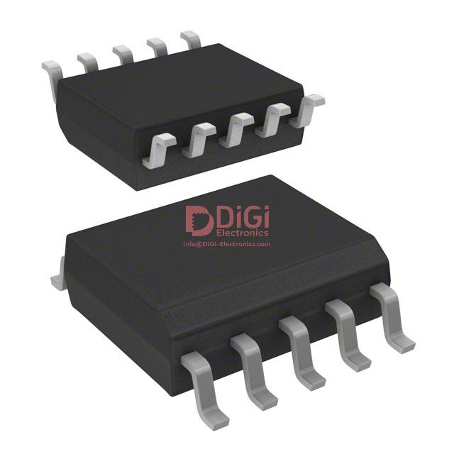
Package details and mounting for VIPER012LSTR
The VIPER012LSTR integrates advanced switching regulator functionalities within an ECOPACK-compliant SSOP10 surface-mount package. This compact form factor directly addresses constraints in board space while maintaining strict adherence to global environmental protocols, making it well-suited for both new designs and green-compliance retrofits. The SSOP10 package, with its controlled lead pitch and mechanical robustness, supports automated pick-and-place processes, reducing assembly defects and improving throughput in high-volume manufacturing.
Mechanical outline specifications are precisely defined to align with industry-standard land patterns, simplifying layout integration and minimizing risk during reflow soldering. Recommended pad geometries not only ensure reliable solder joints but also strategically mitigate the occurrence of tombstoning and other common SMD issues. From a thermal engineering perspective, the package's body dimensions and pin configuration facilitate effective heat dissipation through PCB copper areas, a crucial consideration when deploying the VIPER012LSTR in high-density assemblies or thermally constrained environments such as compact power modules and LED drivers.
Layer stacking and via placement on the PCB play decisive roles in optimizing the thermal flow away from the device. Multiple ground planes beneath the SSOP10, combined with thermal relief on thermal pads, have demonstrated measurable reductions in junction temperature, directly impacting device longevity and reliability. Subtle variations in footprint design, such as slightly enlarging the ground pad or increasing thermal vias, can yield tangible thermal performance gains without adversely affecting assembly yield or electrical characteristics.
Application experiences highlight that, in designs where heat generation is driven primarily by high switching frequencies or elevated ambient temperatures, the recommended land pattern—when coupled with careful placement of thermal vias—provides an effective trade-off between assembly practicality and thermal efficiency. Furthermore, the ECOPACK compliance not only futureproofs designs against regulatory shifts but also simplifies qualification processes for end products targeting international markets.
Integrating VIPER012LSTR in densely populated power topologies underscores the importance of package and footprint synergy with overall thermal management. Such design attention enables aggressive miniaturization without sacrificing electrical or mechanical integrity, an increasingly decisive factor as regulatory, thermal, and productivity constraints converge within modern electronic design. This approach amplifies the package's value proposition beyond its electrical characteristics, positioning it as a reference solution for space-constrained and environmentally sensitive power supply applications.
Potential equivalent/replacement models for VIPER012LSTR
Selecting robust alternatives to the VIPER012LSTR demands a systematic evaluation of both device architecture and application requirements. The primary consideration involves analyzing comparable devices within the STMicroelectronics VIPer01 series, such as the VIPER013 and VIPER014 models. These variants maintain a similar integrated offline converter topology but introduce differences in switching frequency profiles, power handling capability, and available package formats. For instance, a higher switching frequency may enable more compact transformers, useful in space-constrained PCBs, while package options influence thermal management strategies.
Beyond familial alternatives, scrutiny extends to converter ICs offered by leading manufacturers like Texas Instruments, ON Semiconductor, or Infineon. These should be matched on core performance metrics: input voltage range, maximal and minimal output characteristics, quiescent and standby power consumption, and on-chip protection mechanisms. Subtle disparities in start-up current or hiccup-mode fault recovery could be significant, especially in energy-critical or highly reliable designs. Pin-to-pin compatibility warrants special attention, as mismatches may necessitate redesign of PCB layouts or compromise ease of drop-in replacement. Careful reference to detailed datasheets and cross-comparison tables accelerates effective substitution, but nuanced thermal rating and integrated EMI filtering features must also be aligned—small divergences here can impact system longevity or regulatory compliance.
Through close inspection of both electrical and physical specifications, successful transitions hinge on the availability of comprehensive protection features such as overvoltage, overload, thermal shutdown, and brown-out protection. Devices supporting multiple topologies—flyback, buck, or non-isolated arrangements—enhance design flexibility and allow adaptation of existing reference circuits. Temperature derating curves and real-world efficiency data drive selection where operational margins are tight and ambient conditions vary.
Application experience reveals that, in practice, thermal performance and switching noise diverge under load and ambient stress. For example, transitioning from VIPER012LSTR to VIPER013 may present minor PCB tuning requirements due to altered gate drive waveforms, influencing EMI signatures and transformer stress. Adopting an alternative from another vendor often exposes subtle differences in fault response or power-down sequencing, detectable only in stress testing. The most reliable strategy involves staged prototype verification, beginning with electrical parameter simulation and advancing to in-circuit evaluation in the intended end product.
Effective replacement is not solely a function of datasheet parity but an ability to maintain design intent across regulatory, reliability, and manufacturability domains. Experienced practices favor alternatives with proven field history, transparent support resources, and granular configuration options, thereby managing project risk. Value emerges when design decisions account for holistic device behaviors, optimizing for longevity, total cost of ownership, and seamless production transition.
Conclusion
The STMicroelectronics VIPER012LSTR embodies a sophisticated integration of high-voltage startup, onboard control circuitry, and comprehensive protection mechanisms within a compact SMPS controller. Internally, its avalanche-rugged power MOSFET and optimized start-up sequence enable direct connection to rectified AC mains, simplifying initial power architecture. The embedded current-mode PWM controller operates with precise feedback, allowing flexible adaptation to widely used topologies, including flyback and buck converters. This versatility streamlines design iteration, reducing the tuning complexity common in traditional discrete solutions.
Critical to energy efficiency, the VIPER012LSTR incorporates low standby consumption modes and advanced burst operation algorithms. These functions maintain output regulation while curtailing loss during light-load or idle states, directly addressing modern regulatory requirements such as ErP and ENERGY STAR. With only a handful of external passive components—primarily for input filtering and output smoothing—the device accelerates prototyping and minimizes BOM cost without sacrificing operational stability.
Fault tolerance is embedded at multiple levels. Features like output short-circuit protection, thermal shutdown, and automatic restart empower designs to recover gracefully under overload, line surge, or peripheral miswiring events. The controller's immunity to excessive voltage spikes ensures resilience even in electrically harsh environments, supporting long-term reliability in industrial, consumer, and IoT application domains. This reliability aligns with field-tested observations that robust power conversion can be achieved with via careful PCB layout, adequate creepage and clearance around high-voltage pins, and strategic grounding to limit EMI propagation.
Deployment of the VIPER012LSTR further confers ease of international certification. Its compliance with recognized standards reduces the iteration cycle associated with regulatory pre-testing. By leveraging the device's thorough technical documentation, engineers can optimize feedback loop compensation and transformer parameters to precisely balance dynamic response, efficiency, and conducted emissions. Experience in real-world rollouts highlights the value of simulating thermal behavior under maximum ambient conditions during the design phase, as this preemptively identifies needed derating or supplemental heat sinking.
A crucial insight emerges when contrasting generic controllers with this integrated approach: systems designed with the VIPER012LSTR gain a modular power core that scales naturally across power ratings and form factors. The stability inherent in its control algorithms and the breadth of protection mechanisms encourage confident transitioning from prototyping to mass production. As energy codes evolve, such architectures enable rapid compliance adaptation—reaffirming the VIPER012LSTR’s role as a key enabler for next-generation, global-ready, efficient AC-DC conversion systems.


