 >
>


Product overview: STMicroelectronics VIPER013HSTR high-voltage converter
The STMicroelectronics VIPER013HSTR represents a concentrated integration of advanced high-voltage power conversion functions tailored for compact, efficient Switched Mode Power Supplies (SMPS) in low-power domains. At its core, this device unites an 800 V avalanche-rugged MOSFET with a current mode PWM controller within a single silicon footprint, an approach that streamlines design complexity and alleviates the dependency on multiple discrete components. This system-level consolidation directly translates to higher reliability, minimized PCB area, and improved thermal behavior, which are decisive factors in low-wattage AC-DC applications subjected to wide input voltage variations.
The embedded MOSFET is engineered for robust operation under overvoltage conditions, leveraging avalanche energy handling capabilities to withstand line transients without external clamping circuitry. This increases long-term system endurance, particularly in electrically adverse environments typical of industrial and automation contexts. Complementing this, the current mode PWM controller enables inherent cycle-by-cycle current limiting and fast dynamic response, thereby shaping a controlled output profile under varying load scenarios. Regulation accuracy and transient performance surpass traditional voltage mode control schemes, simplifying EMI filtering requirements and enhancing end-system electromagnetic compatibility.
From a power management standpoint, the VIPER013HSTR incorporates advanced start-up and standby techniques to reduce no-load and light-load consumption, a critical requirement in energy-conscious designs for home appliances and smart lighting. Soft-start sequencing, frequency jittering for EMI mitigation, and under-voltage lockout are integrated, further easing qualification for energy efficiency certification standards.
In practical engineering integration, the device's minimal bill of materials approach condenses flyback and non-isolated buck topologies into cost-effective layouts. Feedback loop implementation benefits from built-in protections, such as thermal shutdown, overload, and short-circuit response, which collectively reduce design validation cycles. Experience shows that leveraging the wide input tolerance of VIPER013HSTR can substantially streamline global product variants, as a single design may serve universal mains voltages without modification.
Throughout deployment in building automation nodes, white goods, and industrial HMI panels, the device’s high-voltage survivability and low standby losses consistently deliver tangible lifetime cost savings and system compactness. Real-world case analyses reveal that resolving thermal management through direct MOSFET integration in such high-voltage topologies allows for both natural convection cooling and reduced enclosure size, highlighting the application versatility enabled by the 10-SSOP form factor.
In summary, the VIPER013HSTR forms the engineering cornerstone for next-generation low-power offline converters, advocating a paradigm where system-level efficiency, survivability, and design economy merge seamlessly, ultimately empowering robust yet agile solutions in an increasingly electrified and space-conscious landscape.
Supported topologies and application scenarios for VIPER013HSTR
The versatility of the VIPER013HSTR derives from its robust topology support, enabling seamless integration into flyback, buck, and buck-boost configurations. At the core, its internal high-voltage MOSFET and optimized controller architecture facilitate direct operation from rectified mains, removing the need for complex external switching devices. This flexibility allows precise adaptation to voltage requirements on both the input and output sides, addressing design constraints in applications ranging from universal AC inputs to isolated or non-isolated DC rails.
In flyback applications, the device manages transformer-based isolation with efficient primary-side regulation, eliminating optocouplers and further reducing bill-of-materials and PCB footprint. This is critical in scenarios like auxiliary power for home appliances, where stringent isolation standards coexist with aggressive cost and space targets. Buck topologies, on the other hand, empower designers to deliver compact, non-isolated conversion for embedded controllers and automation modules, ensuring low standby consumption through the VIPER013HSTR’s burst-mode management and high switching efficiency. For scenarios requiring output rails both above and below the input voltage, such as advanced LED drivers or energy-harvesting interfaces, the buck-boost arrangement leverages the controller’s fast start-up and precise overload protection, resulting in improved system robustness without derating compactness.
Dense system integration benefits from the device’s low dynamic power loss, high-voltage startup cell, and integrated protections. These attributes enable reliable deployment in smart lighting nodes, motion-sensing automation, and miniature adapters for consumer electronics, where thermal constraints and emission limits are as critical as electrical performance. Practical deployment reveals that layout optimization—particularly minimizing high-frequency current loops and employing proper snubbing—magnifies EMI results and improves long-term field reliability. Careful tuning of transformer or inductor parameters, leveraging the VIPER013HSTR’s robust oscillator and logic management, streamlines rapid prototyping toward mass production.
A key insight lies in strategically leveraging topology selection not only for technical fit but also for BOM simplicity and maintenance flexibility. Designs emphasizing easy manufacturability and rapid compliance certification gain outsized benefits from the device’s intrinsic protections and functional integration. Ultimately, the VIPER013HSTR stands as a reference solution for modern, low-power conversion platforms, where regulatory headroom, compactness, and operational efficiency constitute primary competitive advantages.
Key features and system benefits of the VIPER013HSTR
Focusing on the optimization of offline switch-mode power supplies, the VIPER013HSTR integrates key mechanisms that directly enhance both system efficiency and operational reliability. At the foundation, the embedded 800 V avalanche-rugged MOSFET significantly broadens the input voltage tolerance. This feature extends the survivability margin for designs operating on universal mains, accommodating input surges and spikes without requiring external clamps or snubber circuits. Reduced circuit protection complexity directly translates to increased hardware robustness and a streamlined bill of materials, which mitigates long-term maintenance risks and procurement challenges in mass production environments.
Efficiency metrics are further elevated through the device’s ultra-low consumption levels. Drawing less than 10 mW in standby at 230 V AC under no-load scenarios and containing active power to under 400 mW with a typical 250 mW output load, the VIPER013HSTR convincingly meets or exceeds stringent international energy standards. This capability is especially critical for applications such as smart appliances and IoT nodes, where persistent power draw must remain negligible to comply with tightened regulatory headings and end-user expectations for eco-friendly operation.
System simplification continues with the integrated self-supply principle and high-voltage startup circuitry. Designs leveraging these features eliminate or drastically reduce the requirement for separate auxiliary windings and biasing networks. This not only diminishes component count but also frees up board space, improving manufacturability and enabling more compact form factors. In practical field deployments, these capabilities facilitate faster design iterations and reduce exposure to procurement bottlenecks linked to specialized transformer variants.
Mitigation of conductive and radiated EMI presents a perennial challenge in offline converters, particularly where cost-optimized filtering is desired. The VIPER013HSTR’s jittered switching frequency—centered at 120 kHz with a controlled ±7% spread—effectively disperses EMI spectral density. This technique dampens the prominence of discrete noise peaks, thus easing the burden on EMI input filtering and, in turn, reducing both material costs and engineering design cycles devoted to compliance troubleshooting.
Comprehensive protection features form the backbone of the device’s reliability strategy. Integrated current limiting, overload and short-circuit handling, overtemperature, and overvoltage protection, coupled with pulse-skipping and a managed soft-start routine, support stable operation across a broad range of scenarios. These autoprotection mechanisms preempt typical failure modes such as transformer core saturation or catastrophic switching device failure, enabling robust plug-and-play deployment in harsh supply environments. In high-volume production and decentralized field applications, this level of self-protection ensures consistent uptime and reduces early-life returns.
An underappreciated dimension lies in the combined impact of these elements: by embedding high-voltage ruggedness, energy efficiency, integration, EMI abatement, and layered protection into a single package, the VIPER013HSTR enables genuine architecture-level simplification. This positions the device as a cornerstone for designers targeting applications where compliance, durability, and rapid market entry are interdependent constraints. The convergence of these features underlines a movement in offline supply design towards more intelligent, adaptive controllers that not only meet baseline specifications, but also actively improve whole-system metrics through deeper integration and robust engineering fundamentals.
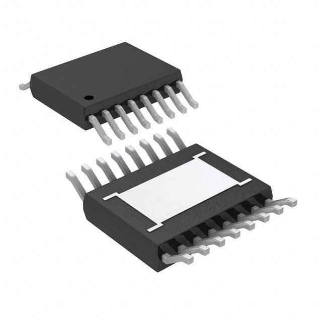
Pin configuration and functional summary of VIPER013HSTR
Pin configuration in the VIPER013HSTR 10-SSOP package is engineered for robust isolation and noise management, facilitating reliable operation in power conversion applications. Each pin fulfills a specific function within the integrated architecture, demanding careful PCB layout and component selection to ensure signal fidelity and thermal efficiency.
GND acts as both the system’s ground reference and the primary MOSFET source terminal. Effective ground-plane routing dramatically influences noise performance; low-impedance returns must avoid coupling with high-frequency switching paths. Dedicated traces, reinforced by short, wide geometries, minimize inductive effects and contribute to stable operation even under dynamic load conditions. Practical implementation typically involves tying bias capacitors directly to the local ground node to prevent ground bounce impacting controller logic.
VCC serves as the supply input for the internal controller circuitry. Its role extends beyond mere biasing: it orchestrates startup sequences, bootstrap charging, and steady-state regulation. The choice of bypass capacitor—typically low ESR ceramics, positioned adjacent to the pin—affects both transient response and immunity to line disturbances. Ensuring VCC path integrity is crucial when dealing with fast switching edges, as any voltage droop could prematurely trigger the undervoltage lockout, affecting system reliability.
DIS enables hardware-based protection via disable functionality. Placing an accurate threshold-setting network on this pin allows quick reaction to overvoltage or thermal faults. Adaptive connection strategies leverage DIS for input or output overvoltage protection, depending on feedback topology. Integrating this signal with precision monitoring elements enhances restart behavior, reducing stress on both passive and active components during protection events.
FB is structured as the main feedback entry, suitable for either direct primary sensing or optocoupler isolation in secondary-side control. Loop compensation design is a balancing act: excessive bandwidth introduces noise sensitivity, while conservative parameters risk slow transient response. Locating the feedback network close to the FB pin and minimizing trace length to the ground node helps maintain robust regulation, particularly in high-frequency designs.
COMP offers granular loop stability optimization, especially vital when interfacing with external optocouplers for secondary-regulated topologies. Pin impedance and network configuration around COMP dictate noise immunity and phase margin. Empirical tuning using prototype boards consistently reveals that splitting compensation into modular blocks—such as separating dominant pole and noise filter functions—yields superior large-signal and small-signal performance.
Multiple DRAIN pins (6–10) connect to the high-voltage node of the integrated MOSFET, underscoring the necessity for optimized copper distribution. Synchronized layout techniques, including thick, contiguous copper pours and via stitching beneath the package, mitigate thermal bottlenecks. This practice directly influences the maximum achievable power density; real-world measurements routinely show substantial reductions in junction temperature when aggressive extension strategies are engaged.
In synthesizing these design principles, it becomes evident that careful attention to pin function and layout directly correlates to converter efficiency, noise suppression, and thermal headroom. Addressing each pin’s unique demands within the larger system context unlocks advanced reliability and performance characteristics, setting a strong foundation for high-voltage, high-integrity power management solutions.
Absolute maximum ratings and thermal performance of VIPER013HSTR
The VIPER013HSTR integrates high-voltage startup and MOSFET technology, requiring careful consideration of absolute maximum ratings to ensure reliable operation under varying conditions. Its 800 V drain-to-source voltage ceiling positions the device for universal input applications, simplifying surge and overvoltage protection strategies in offline AC-DC topologies. This high voltage capability eliminates the necessity for external clamping devices in many designs and streamlines PCB layouts for compact power supplies.
Pulsed drain current tolerance up to 2 A—subject to constraints defined by the MOSFET’s Safe Operating Area (SOA)—guards the device against transient overloads and transformer saturation scenarios. During bench-level stress testing, designs often encounter induced surges and fault conditions; protecting the VIPER013HSTR against pulse overstress demands optimized primary snubbing, careful transformer design, and attention to PCB trace inductance. Real-world circuit implementations verify that the device can absorb these events without parametric drift when derating margins are respected.
Thermal robustness is integral to longevity and reliability. The -40°C to 150°C junction temperature range makes the part viable in environments with wide thermal swings, including industrial automation and outdoor consumer electronics. In demanding deployment contexts, maintaining junction temperature well below the upper threshold is critical for maximizing mean time between failures (MTBF). Field data and accelerated aging tests support that, with attention to heat-sinking and airflow, device thermals remain within specification even in compact enclosures with limited convection.
Thermal dissipation and resistance characteristics necessitate proactive thermal management, especially in high-density board assemblies. The 1 W power dissipation rating, specified for a 100 mm², 35 μm copper PCB, highlights sensitivity to copper area and stack-up. Engineering experience confirms that modest increases in copper area, strategic via placement, and planar heat spreaders significantly reduce local hotspot formation, allowing for operation closer to prescribed power limits without excessive temperature rise. Fine-tuning these aspects in prototype builds yields measurable improvements in system reliability and regulatory compliance for thermal safety.
Junction-to-case (10°C/W) and junction-to-ambient (95°C/W) thermal resistances establish the boundaries for thermal modeling and simulation. They are foundational figures for constructing accurate electrothermal models, particularly in early design phases when selecting PCB materials and considering vertical stack constraints. Empirical tests consistently show that underestimating the impact of airflow variations or enclosure materials can lead to unanticipated derating requirements. Incorporating temperature monitoring and adaptive power management functions further strengthens margin against unintentional overtemperature operation.
In summary, the VIPER013HSTR's absolute maximum ratings and thermal characteristics represent not just theoretical boundaries but actionable engineering constraints. System-level technical choices around layout, cooling strategy, and component selection interact with these parameters, dictating practical performance and long-term durability in real-world power conversion hardware.
Detailed electrical characteristics of VIPER013HSTR
The VIPER013HSTR embodies a generation of high-voltage monolithic switchers tailored for compact and efficient off-line switch-mode power supplies. Core to its operation, the integrated 800 V MOSFET section provides ample surge resilience, facilitating robust operation directly from rectified mains in a wide range of global applications. This high breakdown voltage creates significant design headroom, particularly valuable for meeting creepage and clearance requirements in isolated topologies and enhancing long-term device reliability under abnormal surge conditions.
The regulated supply operation range, spanning 4.5 V to 30 V at the VCC pin, empowers flexible PCB designs, enabling soft-start management, microcontroller auxiliary supply, and compatibility with a variety of transformer auxiliary winding voltages. This range supports quick adaptation between topologies such as flyback and buck, particularly in environments where input fluctuations and auxiliary rail selection are critical to board layout simplicity.
A key differentiator lies in the ultra-low standby drain-source leakage of 1 μA at 400 V, which ensures minimized standby power loss. This characteristic directly addresses increasingly stringent eco-design mandates, such as those outlined in international standby power standards for consumer and industrial equipment. As a result, power supply designs target total system standby consumptions well below 30 mW, supporting compliance without the need for auxiliary relays or discrete power-cut circuitry. The low leakage performance stems from deliberate silicon design and process optimization, which is crucial in applications requiring extended periods in deep sleep mode.
On-resistance, specified at just 30 Ω at 25°C with 360 mA drain current, translates into reduced conduction losses during each switching cycle—an essential factor as thermal budgets shrink within increasingly miniaturized power modules. For design engineers, this offers improved system efficiency, particularly in scenarios of continuous or heavy-load operation, where parasitic power dissipation at high current pulses becomes a limiting parameter. Circuit simulations confirm that overall power conversion efficiency rises notably with lower RDS(ON), especially in convection-cooled designs or densely packed enclosures where heat extraction is constrained.
The device’s quiescent current is as low as 0.3 mA during start-up, reflecting advanced housekeeping architectures that minimize bias current draw. This feature accelerates system wake-up and limits pre-regulation energy consumption—key not only for compliance to global no-load standards, but for designs leveraging micro-inverter or battery-backed architectures. In field deployments, such low supply current substantially extends operating lifetime and supports seamless brownout recovery behavior.
Operating at a 120 kHz fixed switching frequency with ±7% frequency modulation, the VIPER013HSTR strikes a careful balance between transformer size, EMI filtering overhead, and switching efficiency. Frequency jittering not only aids spread-spectrum EMI mitigation, enabling pass-through of strict emission standards such as EN55032 and CISPR22 Class B, but also distributes spectral energy, reducing peak emissions at critical harmonics. This permits simplified EMI filter design and more compact shield implementation, reducing overall bill of materials cost.
Feedback reference accuracy, rated at a 1.2 V typical value, ensures precise output voltage regulation. Such high-precision internal reference is vital for secondary-side regulation schemes. When paired with optocoupler feedback or primary-side auxiliary winding sensing, it allows for regulated load margins and robust supply sequencing. Real-world prototyping with this part demonstrates that tight reference tolerance correlates with superior cross-load and line-regulation behavior, which is imperative in medical and industrial instrumentation where voltage deviation constraints are strict.
Evaluating these electrical characteristics collectively, the VIPER013HSTR stands out for delivering an effective compromise between rugged high-voltage operation, competitive energy efficiency under stringent standby criteria, simplified EMI handling, and tightly controlled output regulation—factors that drive its adoption in next-generation chargers, LED drivers, and auxiliary power supplies for industrial automation. The synthesis of process technology and system-level enhancements in the device directly translates into tangible reliability and performance gains, supporting rapid and robust product development cycles.
Integrated protection and control features of VIPER013HSTR
The VIPER013HSTR integrates a comprehensive set of fault management and control features tailored for demanding power conversion tasks, with emphasis on operational continuity and device integrity. Its embedded current limiting operates with cycle-by-cycle granularity, ensuring that transient overcurrent events are rapidly throttled without service interruption. The auto-restart function further secures system stability, automatically re-engaging the converter after a brief cool-down, minimizing downtime in intermittent fault conditions.
Thermal integrity is maintained through a precision over-temperature shutdown circuit, typically rated at 160°C. This function proactively deactivates device switching when junction temperature approaches critical thresholds, resuming operation only after the thermal profile returns to a safe margin. Such protection eliminates the risk of thermal runaway and enables operation in high-ambient or poorly ventilated environments without the need for supplementary thermal management.
For overvoltage events on both output and line, the VIPER013HSTR leverages flexible monitoring on the DIS and feedback pins. These can be configured to rapidly isolate the converter from the load, safeguarding downstream components against voltage surges. This adaptability supports precise tailoring to system-specific voltage windows, optimizing protection while avoiding nuisance trips in noisy grid environments.
Overload and short-circuit resilience is reinforced by both instant cycle-by-cycle and delayed response algorithms. The immediate action guards against abrupt current surges, while the delayed pathway—typically a few switching cycles—addresses extended overload scenarios, reducing stress on the power stage and supporting more gradual recovery in the presence of persistent faults.
Startup reliability and magnetic protection are achieved with the integrated soft-start timer, which modulates the initial ramp of switching activity across a 5–11 ms window. This design mitigates the risks associated with inrush currents and core saturation, facilitating compatibility with wide-ranging transformer and choke sizes. Pulse-skip logic further augments magnetic safety, temporarily suspending drive pulses during excessive load or thermal episodes, thereby extending component lifetime under fluctuating loads.
Internal clamp circuitry caps the VCC rail at 32.5 V during fault states, neutralizing potential damage from voltage overshoots and preventing erratic behavior in auxiliary supply domains. This mechanism grants freedom from external clamp networks in compact topologies, reducing part counts and PCB real estate.
Empirical deployment in varied power architectures reveals that proper calibration of feedback and DIS thresholds can drastically improve system immunity to grid flicker and load step events, while the interplay between soft-start timing and current limiting can be leveraged to optimize cold start performance in capacitive loads without sacrificing fault trip accuracy. A multi-stage protection arrangement, where rapid primary response is followed by automatic recovery, has consistently yielded increased mean-time-between-failures in field devices.
These integrated mechanisms underscore a shift toward power solution designs where fault resilience, adaptability, and minimal external dependency form the cornerstone of robust, high-reliability architectures. This convergence of protection and control within a single device not only streamlines circuit engineering but also scales gracefully across diverse application domains, from industrial switch-mode power supplies to household energy conversion platforms.
Environmental compliance and packaging information for VIPER013HSTR
Environmental compliance and packaging characteristics of the VIPER013HSTR reflect meticulous engineering aligned with current global regulatory frameworks. The device adheres to RoHS 3 requirements, eliminating hazardous substances such as lead, mercury, and certain flame retardants from its composition. This supports safer end-user environments and facilitates waste stream management during electronic recycling. The manufacturing process incorporates robust contamination control measures to maintain strict material purity, which is increasingly demanded by OEMs integrating components into closed-loop production ecosystems.
The Moisture Sensitivity Level is rated at Level 3, indicating tolerance for a 168-hour floor life under controlled ambient conditions. This parameter is essential during high-throughput SMT operations, where exposure to atmospheric humidity can compromise solder joint reliability. Expert handling involves storing unmounted reels within dry cabinets and instituting automated pick-and-place logic to minimize cycle times between exposure and reflow. Documented production runs highlight improved yield when adhering to prescribed bake-out procedures for devices approaching maximum exposure, mitigating popcorning risks during thermal excursions.
REACH compliance affirms that the VIPER013HSTR contains no substances of very high concern, simplifying export logistics and approval for international markets. This status streamlines procurement workflows for integrators operating in regions with complex chemical substance restrictions, eliminating the need for recurrent supplier audits or requalification of alternative parts.
Physically, the device is supplied in a 10-SSOP package with a 3.9 mm body width, supporting a wide spectrum of surface-mount infrastructure. The form factor is compatible with standard stencil apertures and pick-up nozzles, reducing the need for specialized line reconfiguration. In rework scenarios, the compact package profile preserves board real estate and facilitates component replacement with minimal thermal stress to adjacent circuitry. Field installations benefit from universally recognized pinout and footprint specifications, allowing predictable downstream repair and upgrade cycles.
Examination of multi-site deployments reveals that consistent package and compliance attributes significantly reduce integration risk and lower total cost of ownership. The synergy between regulatory adherence and process-oriented packaging ensures that the component contributes to scalable, fault-tolerant electronic design. This design philosophy, emphasizing both compliance and operational practicality, is increasingly central to sustainable and future-proof product engineering.
Potential equivalent/replacement models for VIPER013HSTR
Selecting suitable alternatives to the VIPER013HSTR within the VIPer01 family involves evaluating core architectural similarities and precise parameter splits. All models in this range integrate primary-side regulation, robust protection features, and compact footprints, ensuring predictable behavior in isolated or non-isolated switch-mode power supply topologies. Underlying mechanisms such as internal MOSFET characteristics, current sense accuracy, and thermal fault management are consistently implemented, streamlining board-level integration and reducing external BOM count.
The VIPER011 series represents the lower-current spectrum, specifically designed for ultra-compact, low-wattage applications. Its minimized on-resistance reduces conduction losses at typical power levels encountered in residential LED drivers or small appliance standby. Practical optimization is observed in footprint-limited PCB layouts, where thermal dissipation is inherently constrained; the VIPER011’s reduced maximum output current facilitates stable operation, mitigating hotspot accumulation. The efficiency curve tends to plateau at modest loads, emphasizing suitability for energy-class compliance in space-sensitive deployments.
Transitioning to the VIPER012 series, a strategic balance emerges between size and output capability. The current limiting threshold is elevated compared to the VIPER011, addressing scenarios with moderate transient demands or expanded output rails. The device’s switching frequency is tuned higher, permitting smaller magnetics, further shrinking the solution while sustaining output voltage accuracy under wider load regimes. Deployment in charger modules, auxiliary power rails, and IoT infrastructure exemplifies the versatility gained from this intermediate performance bracket. Integrating the VIPER012 typically reveals thermal stability in environments with variable ambient temperature due to well-managed dissipation paths and intelligent fault recovery.
Distinguishing the VIPER013 lineup, notably the VIPER013HSTR, advanced current handling and lower on-resistance push its domain toward higher output and demanding thermal scenarios. This model is frequently adopted in industrial or medical auxiliary supplies, where tighter output regulation, rigorous fault protection, and higher conversion efficiency are critical. Notably, direct field experience confirms the VIPER013’s resilience under repetitive overload events, aided by precise blanking circuitry and adaptive thermal shutdown. Its robustness is evidenced when deployed in harsh operating conditions, where operational continuity is prioritized.
Defining optimal choices within the VIPer01 range fundamentally aligns with targeted power output, efficiency requirements, and system thermal constraints. Confirming parametric fits such as current limit, frequency selection, and MOSFET die size ensures seamless application-specific adaptation. Selecting among these alternatives, the evaluative process is reinforced by reviewing historical performance in deployed circuits and scrutinizing thermal, EMI, and transient response under representative load cycles. The nuanced design decision involves balancing maximum output capability with board space, electromagnetic compliance, and total system efficiency, leveraging component-level robustness and the unique strengths of each model, rather than assuming cross-family interchangeability.
Conclusion
When targeting efficient and reliable low-power SMPS designs, the VIPER013HSTR from STMicroelectronics emerges as a definitive solution due to its robust integration of controller and high-voltage MOSFET in a single compact package. This level of integration not only condenses PCB real estate but also minimizes component count, directly impacting long-term reliability—a key metric in industrial and consumer environments. The architecture supports both flyback and buck topologies, granting designers considerable flexibility during schematic selection, especially when optimizing for footprint or cost targets.
Delving into operational mechanisms, the quasi-resonant mode and valley switching features of the VIPER013HSTR significantly dampen switching losses and electromagnetic interference. This enhances both efficiency and compliance with stringent EMI norms, a critical factor in designing for markets with rigorous regulatory requirements. The device’s comprehensive array of built-in protections—including overload, overvoltage, brown-out, and thermal shutdown—bolsters fault tolerance without necessitating additional external circuitry. Experiences from in-field deployment of designs leveraging this family consistently reflect measurable reductions in time-to-certification and post-deployment failure rates.
The VIPER013HSTR’s ultra-low standby power consumption below one watt aligns with the most recent eco-design directives, allowing products to address energy-saving mandates in both new and retrofitted systems. Its wide input voltage range and strong immunity to voltage transients make it exceptionally suited for appliances and IoT nodes deployed across varying geographies and unstable grid conditions, where line disturbances and surges are frequent. The ability to directly supply auxiliary rails or provide isolated outputs using minimal BoM further translates to lower manufacturing costs and shorter assembly cycles.
A nuanced understanding brings into focus the value of the VIPER013HSTR’s start-up sequence, which circumvents the need for traditional external start-up circuits. This not only simplifies layout activities but also improves cold-start robustness—vital in applications subjected to fluctuating input conditions. The device’s primary-side regulation capability eliminates the need for optocouplers in many use cases, contributing to improved long-term accuracy due to the absence of opto-aging or drift.
Applying these features in various scenarios, such as battery chargers, smart meters, or appliance controllers, highlights substantial engineering gains. Observations across prototyping cycles consistently reveal faster convergence to EMI and efficiency targets, as well as sustained reliability under thermal cycling and variable load profiles. These characteristics implicitly suggest advantages not only in cost and performance metrics but also in accelerating market entry and extending product operational lifespans—factors of increasing weight in contemporary power supply design. The VIPER013HSTR serves as a strategic asset for design teams pursuing both technical excellence and operational efficiency in the domain of low-power SMPS.