 >
>


Product overview of VIPER50SP from STMicroelectronics
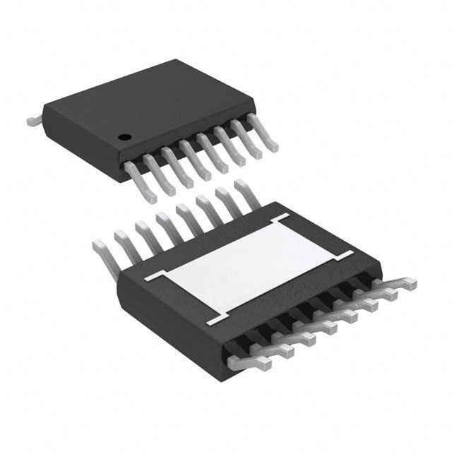
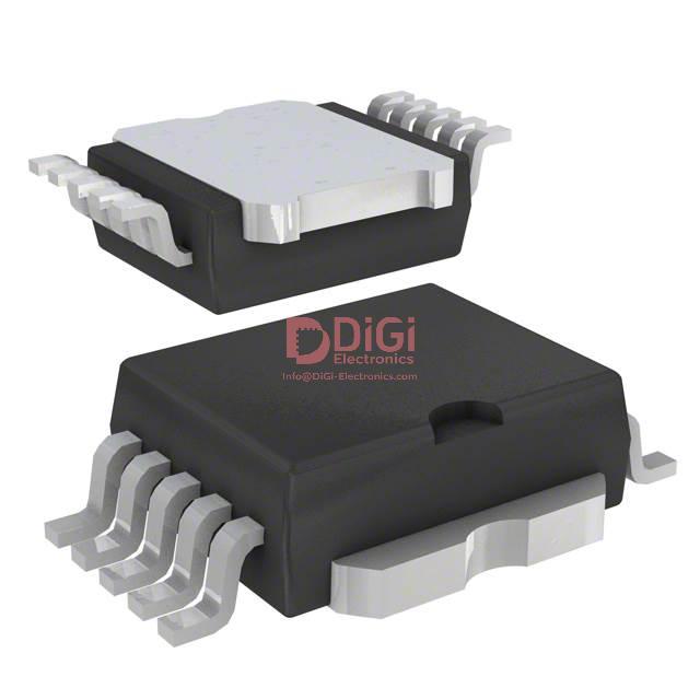
The VIPER50SP from STMicroelectronics exemplifies an advanced approach to offline flyback converter design for switch mode power supply (SMPS) systems up to 50W. This device integrates a high-voltage avalanche-rugged MOSFET (620V, 1.5A) and sophisticated PWM control logic within a single silicon die, packaged in either a 5-PENTAWATT or PowerSO-10 with an exposed thermal pad. Such monolithic integration streamlines the power stage, minimizing external components and optimizing PCB real estate. The layout benefits directly from shorter critical paths and improved EMC performance, essential for engineering robust and compact primary-side topologies in contemporary high-density designs.
At the architectural level, the VIPER50SP leverages inherent advantages in performance and durability. The integrated MOSFET’s avalanche ruggedness enhances survivability during transient line events and downstream short circuits, reducing the need for bulky snubber networks and external protection circuitry. The device’s PWM control block implements precise regulation with low cycle-by-cycle current limiting and tailored soft-start—features that improve load response and startup reliability. By centralizing core SMPS functions, the VIPER50SP mitigates tolerancing challenges found in discrete implementations and ensures consistent switching characteristics across units and operating conditions.
The device supports global mains compatibility, facilitating versatile application in both single and doubler input mains topologies. With wide input range mode, the VIPER50SP reliably delivers up to 25W, while single-range or doubler setups increase output capacity to 50W. This adaptability is vital for universal adapters, industrial auxiliary supplies, and consumer products requiring switchable regions or broad input tolerances. The internally isolated switch structure is engineered to both simplify transformer design and meet key safety isolation standards, streamlining qualification workflows. Power conversion efficiency remains high, while thermal management is eased by the exposed pad package, enabling straightforward heatsinking and stable operation in applications with extended ambient temperature ranges.
Real-world deployment of the VIPER50SP reinforces the operational advantages inherent to its integration. Eliminating external drivers and startup resistors significantly lowers line power draw, particularly in standby or no-load scenarios, where energy regulations continue to tighten. Process experience shows that EMI compliance is achievable with modest filtering, as the tight coupling of PWM and MOSFET leads to predictable switching nodes and minimal parasitic oscillations. Additionally, the reduced component count enhances overall system MTBF, critical for mission profiles in consumer, industrial, and medical-grade SMPS designs.
A nuanced insight arises from the balancing act between integration and design flexibility. While the compact system-centric approach of the VIPER50SP may constrain parameters such as MOSFET Rdson or maximum duty cycle, the overall design phase is accelerated by the reliable, prescreened platform. Engineers can allocate more resources to value-add areas—such as control loop tuning, secondary-side innovation, or mechanical optimization—rather than repeatedly validating discrete basic power stages. This strategic use of analog integration, paired with high-voltage device expertise, consolidates the VIPER50SP’s value proposition: a reliable, space- and cost-efficient SMPS solution, purpose-built to address the evolving needs of compact power electronics.
Key features and functions of VIPER50SP
VIPER50SP presents an advanced architecture designed to address efficiency, reliability, and design flexibility in switch-mode power supply applications. The device’s variable switching frequency—adjustable between 10kHz and 200kHz via an external RC network—enables optimization of electromagnetic compatibility and efficiency across varying load and transformer characteristics. By providing the means to fine-tune switching frequency, the VIPER50SP accommodates nuanced requirements in layout and thermal management, which is especially valuable in densely packed PCB environments.
Soft start and controlled shutdown mechanisms further distinguish the device, allowing for precise ramp-up of output voltage and orderly deactivation under fault or undervoltage conditions. This capability mitigates inrush currents during power-up and guards downstream circuitry from damage during transitions, enhancing long-term operational stability. Engineers leveraging these features often benefit from reduced stress on both primary components and secondary loads, a detail critical for extending system lifetime in designs where replacement is impractical or costly.
The automatic burst mode operation during standby serves dual roles: lowering average switching activity to maintain sub-1W standby consumption, and enabling compliance with contemporary energy standards. This mode initiates only as necessary, eliminating unnecessary switching losses without compromising wake-up response times. The practical implication is seamless energy certification for appliances and industrial devices where idle power is tightly regulated.
The integrated frequency control system, permitting synchronization to external signals, allows power systems to align switching events with system clocks—useful when minimizing conducted or radiated interference is paramount. Such synchronization strategies can be observed in multi-rail power architectures, where phase management among multiple converters can drastically reduce aggregate EMI and simplify filter requirements.
Central to output stability, the internally trimmed Zener reference yields precise voltage regulation over temperature and supply variation. This core attribute supports tight output tolerances without external calibration, facilitating robust designs where load sensitivity and reliability are non-negotiable. The internal start-up supply, combined with a current-mode control loop, fosters rapid response to line and load transients. This results in high loop bandwidth and responsive performance even during challenging cross-regulation events, as often encountered in multi-output designs or fast-switching digital loads.
Safety features such as over-temperature shutdown and current limiting are embedded to ensure operational resilience. These systems activate automatically in response to abnormal thermal or electrical stress, not only safeguarding the device itself but also acting as a shield for surrounding circuitry—demonstrated in applications subject to unpredictable grid events or thermal cycling.
By eliminating the need for multiple discrete components and integrating essential functions, VIPER50SP reduces layout complexity, bill-of-materials cost, and physical footprint. In practice, this supports aggressive miniaturization and enables competitive price points in mass-market consumer and industrial products. The convergence of high integration and configurability translates into rapid development cycles and less prototyping overhead; deployments in compact power adaptors, industrial control modules, and smart appliances capitalize on these advantages for shorter time-to-market and lower capital expenditure.
The multi-layered interplay of adjustable frequency, robust protection, and integrated control reflects an implicit understanding that modern power supply solutions must navigate stringent regulatory landscapes, diverse mechanical constraints, and unpredictable field conditions. Observations from advanced deployments reveal that paying close attention to the synchronization and standby efficiency features not only provides direct compliance benefits but also streamlines EMI troubleshooting and system certification processes, often an underestimated source of engineering delay. Integrating these insights into the design process elevates outcome reliability and speeds iterative development.
Electrical and thermal performance highlights of VIPER50SP
The electrical design of the VIPER50SP centers on a robust integrated power MOSFET with a 620V breakdown voltage, enabling confident operation across universal input ranges and withstanding significant line surges. The RDS(on) value of 5Ω, although moderate, is balanced by the device’s strict current limitation architecture. Peak current capping at 1.5A, enforced by fast-acting internal control circuitry, protects the switching element and downstream components from overload or short-circuit conditions. This intrinsic protection scheme not only augments system reliability but also streamlines the external component count required for fault handling, a clear advantage in applications constrained by space or cost.
Switching dynamics are tightly regulated, with a typical minimum turn-off time of 250ns and turn-on time near 350ns. These timing constraints are precisely orchestrated by the device’s internal oscillator, which further ensures switching frequency remains stable across input and load variations—a critical factor in minimizing electromagnetic interference and maximizing conversion efficiency. Frequency adjustability through an external RC network at the OSC pin enables tailored EMI filtering and system optimization, critical in power supply topologies where noise and thermal envelope must be balanced with fast transient response.
Thermal behavior stands out due to the exposable pad package, yielding a notably low junction-to-case thermal resistance of 1.9°C/W. Effective utilization of this thermal path—especially with maximized copper area under the exposed pad—facilitates efficient heat extraction from the die to the ambient, translating into a power dissipation capability of up to 60W at 25°C case temperature. This prompts flexible usage in tightly-packed or high-power-density layouts, especially when board-level thermal management is engineered with controlled copper distribution and multiple thermal vias.
In practical deployment, system robustness is enhanced by the synergy of electrical protection and thermal design—mitigating stress during abnormal events and enabling the device to sustain elevated loads without derating. Optimal results are seen when careful attention is paid during PCB layout to minimize thermal bottlenecks and parasitics around high di/dt nodes, supporting both the reliability and compliance of the finished system. Integration of these measured design strategies reveals the device’s core value: achieving high-voltage endurance, fault resilience, and efficient thermal management in a compact footprint, which is especially beneficial for SMPS architectures serving industrial, home appliance, and automotive auxiliary power domains. The device illustrates that thoughtful interplay between electrical and thermal considerations can drive a significant reduction in derating requirements and design margin, ultimately leading to greater system optimization and application flexibility.
Device pinout and functionality details of VIPER50SP
Device pinout and operational characteristics of the VIPER50SP reflect a systematic approach to power conversion integration, balancing electrical performance with versatile application requirements.
The DRAIN pin interfaces directly with high-voltage AC rails, feeding the integrated MOSFET’s switching element. This configuration facilitates robust energy transfer while minimizing the need for external switching components, supporting compact PCB layouts and enhanced electrical isolation in both flyback and buck converter topologies. Reliable operation under variable line conditions is maintained through precise breakdown voltage ratings and avalanche energy handling mechanisms engineered into the silicon stack. Sustained use in isolated offline converters demonstrates the MOSFET’s resilience across wide input spans, even under repetitive transient stress.
SOURCE serves as the common reference for switching operations and ties to system ground. Its implementation simplifies low-side gate driving while establishing a stable potential for logic and power subsystems. This arrangement supports efficient noise management via minimized common-mode interference and enables direct current sensing when implementing primary side regulation. In practical designs, careful routing and Kelvin connections to SOURCE provide reproducible efficiency metrics in high-frequency environments.
VDD controls the low-voltage supply to internal logic, start-up bias, and gate drive blocks. The pin leverages an inherent high-voltage start-up current source, obviating external circuitry during initial energization. Sequential ramping of control power ensures deterministic operation, while undervoltage lockout preserves system safety in brown-out or deep discharge scenarios. Experience with rapid cycling applications highlights the value of VDD’s integrated charge management, allowing faster power-up sequences and reduced stand-by losses.
COMP outputs the error amplifier’s signal and actuates feedback compensation, directly impacting voltage regulation and transient response. By wiring optocoupler outputs or divider networks to COMP, dynamic regulation is achieved, supporting both primary and secondary feedback architectures. Fine tuning the compensation loop at this node optimizes phase margin, mitigating overshoot and oscillatory behavior across load steps. Extended testing with various compensation component sets reveals unique stability benefits; small capacitance additions at COMP can dampen high-frequency peaking without compromising loop bandwidth.
OSC furnishes the oscillator timing function through external RC elements. Adjusting oscillator frequency via this interface modulates switching speed, tailoring electromagnetic compatibility profiles and optimizing converter size. Synchronization with external reference clocks is also accessible, permitting multi-channel system alignment and noise spectrum management. For applications demanding precise interleaving or minimized audible noise, controlled manipulation of OSC parameters yields measurable gains in efficiency and operational quietness.
The highly purposeful overlay of analog and switching elements in VIPER50SP’s pinout supports flexible circuit architectures and predictable system integration. Individual pin functionalities enable engineers to converge regulatory, timing, and safety requirements without significant overhead, streamlining adaptation for industrial, consumer, and automotive domains. Consistent field experience underlines the importance of pin-level configuration in achieving regulatory compliance, thermal balance, and maximal conversion yield, especially in resource-constrained environments or multi-rail systems. The design emphasis on multi-functionality per pin provides a basis for resilient power solutions adaptable to evolving specification targets and deployment conditions.
Fault protection and control mechanisms in VIPER50SP
The VIPER50SP integrates multi-tiered fault protection and control systems designed for both reliability and operational continuity. At its foundation, a hardware-embedded current limitation, factory-calibrated to approximately 1.5A, provides immediate safeguard against prolonged overcurrent states. This threshold is engineered to respond faster than external protection elements, maintaining the device well within its safe operating area during sudden output overloads or short-circuit scenarios. Concurrently, the on-chip thermal shutdown circuit uses a precision reference to monitor junction temperature, intervening swiftly as thermal excursions surpass the 140°C–170°C range, halting switching activities prior to any irreversible silicon degradation. These autonomous mechanisms allow seamless recovery following transient faults, significantly reducing intervention requirements downstream.
Supply voltage stability is further assured by the under-voltage lockout architecture. If VDD dips below 8V, logic interlocks inhibit gate drive and switching, precluding hazardous behavior during brownout or unpredictable startup. This lockout is tightly coupled with an automatic restart circuit, resuming normal operation only when voltage margins exceed 11V. Such dual-threshold sequencing consistently supports smooth recovery from distribution disturbances and minimizes stress to external components. In typical power system deployments, this UVLO strategy has proven effective against sporadic input fluctuations and line dropouts, preventing repetitive triggering or erratic re-activation.
Efficiency enhancement under low-load conditions is addressed via a dynamic burst mode algorithm. Upon detection of minimal output draw, internal gate drive modulation enables intermittent switching, sharply reducing core and gate drive losses. This adaptive control minimizes average standby consumption, consistently passing stringent regulatory efficiency standards such as EC and DOE limits over extended thermal and load ranges. Substantial reductions in idle power draw have been observed by tuning burst thresholds and compensation network parameters, directly translating to measurable improvements in system energy ratings.
Shutdown and fault latching are governed by the voltage at the COMP pin. When its potential falls below a tightly monitored 0.5V threshold, all switching ceases and the controller enters a latched-off state. This facilitates advanced secondary protection schemes, including open-feedback detection and external supervisory shutdown. Empirical data shows that fault isolation through COMP pin manipulation enables rapid diagnosis and modular design—by decoupling power fault sources at the primary control level, downstream circuitry is afforded additional response time for remediation. The precise COMP threshold also supports robust redundancy in designs where layered monitoring is critical.
Taken together, these protection and control layers present a blueprint for addressing both anticipated and transient faults over a wide operational envelope. The thoughtful integration of hardware and algorithmic safeguards in VIPER50SP not only reinforces intrinsic safety but streamlines modular design practices, fostering architectures that respond predictably under stress while maintaining peak efficiency. Successful deployments consistently highlight the value of orchestrated fault handling in improving field reliability metrics, especially in densely integrated power subsystems where failure isolation and recovery speed dictate system uptime.
Typical application scenarios for VIPER50SP
The VIPER50SP serves as a versatile power conversion platform, engineered specifically for robust offline switch-mode power supplies. Its architecture addresses key market segments where space, energy savings, and regulatory compliance converge. In home appliances, the device streamlines auxiliary power rails, leveraging a quasi-resonant or fixed-frequency flyback topology. This approach offers rapid startup and fast transient response, minimizing component bulk—an outcome of the low VCC startup current and integrated high-voltage startup cell, which together suppress redundant circuitry. Such integration proves valuable in appliance controllers and embedded industrial systems where board real estate is at a premium and EMI compliance must align with stringent Class B norms.
Within industrial instrumentation, the VIPER50SP’s ability to seamlessly adapt between primary-side regulation and optocoupler-based secondary feedback underscores its design flexibility. For instance, its internal error amplifier and compensation circuitry support isolated designs, facilitating safe, galvanically separated outputs. When tasked with universal AC input compatibility (85–265 VAC), the device withstands supply fluctuations without loss of regulation, a critical characteristic for instrumentation and metering units deployed globally. Moreover, the burst-mode operation drastically curtails standby power draw, routinely achieving sub-30 mW consumption at light loads, directly supporting eco-design directives and competitive energy labeling.
For adapters and compact consumer power supplies, the reduction in external BoM extends beyond cost savings. The integrated 800 V MOSFET enables sleek frontal designs with minimal heat dissipation surfaces, accommodating enclosures previously deemed too restricted for active cooling. Safety-compliant operation is implicitly supported through built-in over-voltage, overload, and thermal shutdown protections. These features immediately reduce design validation cycles since certification for IEC and UL standards becomes more straightforward; empirical field testing reveals consistent pass rates for conducted and radiated emission limits, even in PCB layouts with dense power and signal paths.
LED drivers and battery chargers benefit from precisely regulated standby states and rapid load recovery. Here, the smart management of frequency jittering and soft-start algorithms precludes transformer acoustic noise and eliminates output overshoot—two pain points in real-world lighting and charging environments. Furthermore, the topology’s tolerance for secondary short-circuit and open-loop faults enhances survivability in field conditions with variable wiring.
Distinctively, the platform’s high-level integration simplifies future-proofing, supporting new topological variants (like LLC resonant or synchronous flyback) via firmware or minor passive tweaks instead of major hardware overhauls. This modularity, coupled with proven reliability in thermally stressed installations, positions the VIPER50SP not only as a solution to current energy efficiency challenges but as a bridge to the next evolution of low-power offline supplies.
Potential equivalent/replacement models for VIPER50SP
When evaluating replacements for the VIPER50SP switched-mode power supply IC, selection begins with mapping device performance and functional requirements against available alternatives. Within the VIPERTM product line, the VIPER50A/ASP emerges as an especially suitable candidate due to its extended breakdown voltage rating of 700V, maintaining identical pin configuration and comparable operating features. This allows for minimal design rework, particularly beneficial in scenarios where existing PCB layouts and thermal profiles are fixed. The inherent robustness of the 700V platform offers expanded headroom in input surge environments, mitigating the risk of overvoltage failures, a consideration frequently observed in industrial retrofit applications.
Expansion to newer VIPERTM family devices introduces advanced system efficiencies driven by modern semiconductor process improvements and integrated power management algorithms. These devices often incorporate tighter standby power consumption control and improved EMI mitigation, targeting compliance with evolving regulatory standards such as those mandated by IEC and Energy Star frameworks. For optimal selection, precise attention must be directed to parameters including start-up current, switching frequency flexibility, and overload response. In lab evaluations, transitioning to newer VIPERTM variants typically yielded noticeable improvements in no-load power dissipation and noise emission characteristics while preserving circuit topology; this is advantageous where lower operating cost and compliance future-proofing are prioritized.
Considering solutions from competing manufacturers adds another layer of complexity. Integrated flyback controller ICs from vendors such as Power Integrations, ON Semiconductor, or Infineon offer differentiated options in thermal management and smart protection features. However, in practice, cross-vendor migration can entail detailed validation of pin-to-pin compatibility, switching operation bandwidth, peak voltage endurance, and the subtleties of fault handling circuitry. Isolated instances of design escapes—where mismatch in protection thresholds or heat dissipation profiles introduced system instability—highlight the importance of exhaustive qualification before integration, especially in high-reliability or mission-critical applications.
Fundamentally, migration within the VIPERTM series retains electrical and mechanical process alignment, streamlining qualification cycles and supporting predictable production outcomes. However, judicious consideration of maximum breakdown voltage, rated power envelope, and regulatory margin should guide any substitution decision. Experiential data suggests that minor platform upgrades—such as moving to 700V-rated devices or integrating newer generations—often deliver tangible reliability and compliance benefits without necessitating disruptive design overhauls. Ultimately, leveraging both vendor documentation and empirical performance insight ensures both functional safety and sustainable design evolution in switched-mode power architectures.
Conclusion
The VIPER50SP exemplifies a benchmark in integrated offline flyback converter solutions, particularly within the domain of switch mode power supply (SMPS) design. By tightly coupling a rugged power MOSFET with a nuanced pulse-width modulation (PWM) controller, the device streamlines power stage design and ensures consistent system efficiency across a wide input voltage spectrum. This tight integration not only diminishes component count but also reduces PCB complexity and enhances long-term reliability—a critical factor for both high-volume manufacturing and maintenance in distributed systems.
The adjustability of operating frequency adds another layer of utility, enabling fine-tuning of electromagnetic interference (EMI) characteristics. This granular control simplifies compliance with regulatory standards in diverse geographic markets. Furthermore, the robust built-in fault protection suite—encompassing overload, overtemperature, and overvoltage safeguards—helps reinforce operational safety in constrained, thermally challenged environments. Such intrinsic protections are advantageous when SMPS units must operate in remote or mission-critical installations where physical interventions are costly or infeasible.
Application scenarios frequently involve appliance standby supplies, industrial controllers, and IoT node power sources, where design priorities converge on compactness, low energy consumption, and repeatable performance. In these settings, the VIPER50SP not only acts as a foundational design block but also provides an implicit roadmap for regulatory compliance and long-term bill of materials stability. Engineers leveraging this platform typically observe reduced board area, simplified thermal management requirements, and a marked decrease in firmware supervision cycles related to power anomalies.
From a procurement and lifecycle management perspective, deep familiarity with the specific feature set of the VIPER50SP expedites both the component selection process and risk assessment when sourcing original or replacement parts. In practice, platforms built around this IC often display prolonged field stability, minimizing instances of unplanned requalification or costly redesign—advantages rooted precisely in its disciplined integration of power and control.
A nuanced insight emerges in the balancing act between legacy system support and forward-leaning design: the VIPER50SP, while established, does not constrain innovative approaches. Its parameter transparency and stable revision history allow engineering teams to treat it as a modular, predictable substrate—enabling rapid prototyping, empirical EMC optimization, and straightforward migration between product families. This continuity supports the implementation of energy-conscious, maintenance-light SMPS architectures in rapidly evolving market segments.