 >
>


Product overview – VIPER013XSTR
The VIPER013XSTR represents a significant advancement in offline high-voltage conversion, leveraging integration to streamline SMPS designs where space, efficiency, and reliability are paramount. Central to its architecture is the seamless combination of an 800 V avalanche-rugged power MOSFET and a current-mode PWM controller, housed within a compact 10-SSOP form factor. This device consolidates circuitry that traditionally demands substantial PCB real estate, notably reducing external component count and enabling denser designs—essential for embedded power stages in modern appliances or industrial modules.
Analysis of the embedded high-voltage startup cell reveals an engineering-driven emphasis on rapid, reliable initial power sequencing directly from the supply rail. This feature ensures ultralow standby power capability by minimizing startup resistive losses, a key requirement as regulatory mandates tighten on standby consumption for consumer and industrial equipment. The high-voltage startup further facilitates efficient cold-start behavior, supporting trouble-free operation across a wide range of input conditions without auxiliary biasing, which expedites both design and compliance validation cycles.
In operation, the peak-current-mode control topology enables precise output regulation and rapid transient response, critical for dynamic load conditions typical in lighting ballasts or home appliances with variable motor drives. This approach simplifies loop compensation and augments immunity against line perturbations, reducing EMI design challenges. Integrated protection functions—including over-temperature, overload, over-voltage, and short-circuit safeguards—are hardwired, furnishing robust fault tolerance without the risk of microcontroller lockup or software dependencies. These attributes collectively enhance the Mean Time Between Failures (MTBF), a nonnegotiable metric in safety-focused or maintenance-averse deployments.
Translating device capabilities into application-level benefits, the VIPER013XSTR readily addresses the miniaturization trend in power modules, supporting direct integration into smart actuator nodes, LED drivers, or single-board home automation controllers. The device's high integration yields consistent assembly outcomes and enables economies of scale through BOM consolidation. During implementation, the onboard protections and inherently stable control response alleviate iterative board spins for margin tuning—an efficiency not always achieved with discrete multi-IC solutions.
At a broader level, its design philosophy embodies a forward-compatible approach, anticipating stricter energy standards and the proliferation of always-on smart systems. Its synergistic integration of high-voltage switching, precise regulation, and uncompromising protections not only streamlines the engineering workflow but also lays a robust foundation for power platforms across diverse sectors. This architecture bridges the persistent industry demand for ever-smaller, safer, and more energy-efficient power conversion—delivering both immediate engineering efficiencies and longer-term product lifecycle advantages.
Key features and technology highlights – VIPER013XSTR
The VIPER013XSTR distinguishes itself through a structural emphasis on high integration, directly targeting constraints faced in compact, cost-sensitive power conversion. At its core, the integration of an 800 V avalanche-rugged power MOSFET with the current mode PWM controller provides a robust platform that absorbs wide voltage swings and surges at the AC input. This capability supports global mains compatibility and withstands abnormal line events, which is crucial in geographically diverse applications and demanding industrial environments.
The embedded high-voltage startup mechanism, paired with a proprietary sense-FET architecture, contributes to substantial external component reduction. This not only curtails bill of materials costs but also directly impacts board real estate, yielding design flexibility—particularly valuable in high-density or thermally constrained layouts. By omitting auxiliary bias windings through self-supply, the controller eliminates traditional sources of standby losses and circuit complexity, streamlining magnetics selection and wiring while preventing typical startup circuitry failures found in discrete approaches.
Efficiency in ultra-light load and standby modes represents another engineering highlight. The chipset maintains input power well below 10 mW under no-load at 230 VAC, and under 400 mW when lightly loaded. This is accomplished by fine-tuned internal bias paths and pulse-frequency modulation control at low loads, supporting compliance with global ecodesign directives. Practical deployment demonstrates that such low standby consumption translates to system-level energy savings, especially in always-on consumer appliances or auxiliary-powered industrial modules where cumulative running costs are significant.
Electromagnetic compatibility is enhanced through jittered switching frequency options. The fixed-frequency oscillator, spread ±7% around nominal points (30 kHz, 60 kHz, 120 kHz), diffuses spectral energy and measurably reduces peak EMI emissions. This approach simplifies filter design, sometimes obviating bulky common-mode chokes and facilitating certification in cost-constrained products. Field implementations consistently observe minimized conducted and radiated noise without adverse impact on regulation or transient response.
The inclusion of a precise, embedded transconductance error amplifier with a stable 1.2 V reference underpins flexible feedback handling. Both primary and secondary side regulation topologies are addressed, allowing adaptation from simple standalone flyback designs to opto-coupled isolated supplies. Real-world adjustments to compensation networks and feedback coupling are rendered straightforward, due to the amplifier's fast settling times and minimal offset, allowing for rapid product customization or tuning across multiple power profiles.
Protection logic is both comprehensive and granular. Fast-acting overcurrent and overload/short-circuit detection supplement traditional open-loop and overvoltage thresholds; the max duty cycle counter and pulse-skipping controls prevent magnetic component overstress and minimize acoustic noise during transients or load steps. The soft-start sequencing and thermal shutdown further enhance system robustness. Empirical testing in harsh operating conditions verifies thermal cycling stability and recovery from abusive line events, reducing field failure rates and warranty incidence.
A nuanced observation from laboratory deployment highlights the soft-start and PFM block’s critical role in both noise abatement and transformer stress reduction. Slow ramping of pulse duty stabilizes magnetic flux, while variable frequency operation at light load diminishes audible noise and curtails core losses—a strategic advantage for designs targeting stringent acoustic footprints, such as in medical or domestic environments.
Synthesizing these features, the VIPER013XSTR establishes a platform that transcends incremental improvement, instead forging a pathway to minimized external circuitry, scalable global designs, and superior regulatory compliance. This approach aligns with an emerging paradigm that prioritizes energy savings and operational resilience without incurring penalties in design flexibility or manufacturability. Such architectural consolidation, coupled with robust self-protection, is poised to redefine expectations for low-power offline converters in both legacy and next-generation supply architectures.
Typical operating scenarios and applications – VIPER013XSTR
VIPER013XSTR integrates versatile control and protection features which position it as an optimal solution for a wide spectrum of low power AC-DC conversion requirements. At its core, the device embeds a high-voltage startup cell, PWM controller, and a 730V power MOSFET within a single compact package. This integration significantly reduces external component count, allowing for minimized PCB footprints—a decisive advantage where layout constraints and BOM cost optimization are critical.
From a topology perspective, the VIPER013XSTR supports both isolated and non-isolated flyback architectures, enabling flexible adaptations to diverse isolation and voltage output demands. Its capability to also configure buck and buck-boost circuits expands design latitude, accommodating varying input voltage ranges and output power requirements without complex redesign. This adaptability simplifies inventory management and accelerates time-to-market by standardizing the power stage across multiple products.
In home and building automation controllers, the VIPER013XSTR enables always-on SMPS designs where ultra-low standby consumption is mandatory. Rigorous European and global regulatory frameworks necessitate standby power below 0.5W, and the integrated high-voltage startup—with low quiescent consumption in burst mode—directly targets this constraint. These characteristics also filter into the appliance domain, where energy labels drive manufacturers toward elevated seasonal efficiency standards.
Low power adapters for consumer electronics leverage the VIPER013XSTR’s built-in protection mechanisms—overload, overvoltage, and thermal shutdown—to enhance field reliability while maintaining design simplicity. Even in USB or small form factor power supplies, noise-sensitive applications benefit from the device’s spread spectrum frequency modulation, limiting electromagnetic interference and easing the EMC qualification process. The reduction in bill-of-materials complexity further translates into improved manufacturability and yield.
In industrial and commercial sectors, LED lighting drivers and motion control systems require robust operation under fluctuating AC mains conditions. Here, the VIPER013XSTR’s integrated high-voltage MOSFET ensures wide input tolerance and robust transient handling. Its support for both constant voltage and constant current regulation modes caters to diverse end uses, such as powering LED strings or small actuators. The internal protection logic shields the power stage from common failure modes—an essential consideration where maintenance access is restricted and equipment uptime is paramount.
Overall, the VIPER013XSTR’s feature set aligns closely with the trend toward denser, more efficient, and standards-compliant low power power supplies. The device streamlines the engineering workflow by masking system-level complexity and embedding proven control intelligence, alleviating common design pitfalls such as loop instability and thermal margins. Its architecture anticipates evolving legislation on energy efficiency, while the integrated approach offers resilience and operational grace in real-world application envelopes. With these factors, migration toward such highly integrated AC-DC controllers is both a rational and forward-compatible step in modern power electronics design.
Electrical and thermal characteristics – VIPER013XSTR
Electrical and thermal performance of the VIPER013XSTR is defined through a well-engineered set of specifications targeting high-voltage, efficient power conversion environments. At the core lies the device’s integrated avalanche-rated power MOSFET, supporting drain-source voltages up to 800 V. The combination of low maximum RDS(ON) at 20 Ω and a precisely controlled current limit (IDLIM) fosters consistent switching characteristics under both normal and transient conditions. This contributes to robust fault tolerance, especially during line surges or load anomalies.
Wide VCC operation, spanning 4.5 V to 30 V, enhances compatibility with diverse supply configurations, broadening deployment flexibility in adapter, industrial control, and auxiliary power scenarios. The device’s typical temperature range, from -40°C to 125°C, aligns with harsh environments, while internal protection mechanisms maintain electrical stability under varying thermal stress. At the board level, thermal resistance metrics—benchmarked on standard FR4 PCB layouts—enable streamlined thermal management through ordinary copper layouts and natural convection. This aspect is critical in practical designs, where layout constraints strongly influence junction temperature and long-term reliability.
The ability to sustain steady power output within defined wattage bands—optimally suited to low and medium wattage applications—is achieved through detailed power de-rating guidance. Direct reference to thermal de-rating tables informs design trade-offs, allowing precise calculation of safe operating areas as environmental conditions and enclosure characteristics fluctuate.
Datasheet performance curves, derived from empirical validation under temperature sweep and load step testing, show limited drift in key parameters. This stability is engineered by the tight tolerance of process control and material selection. Such predictability permits system designers to confidently integrate the VIPER013XSTR into applications where long-term power supply reliability is non-negotiable.
Layered analysis of power conversion devices like the VIPER013XSTR reveals a foundational interplay between semiconductor integrity, thermal dissipation pathways, and external conditions. Efficient thermal design, using appropriate copper pours and strategic component placement, ensures the device can sustain its rated current without triggering protective shutdowns. Experience underscores the importance of synchronizing electrical protection with thermal budget constraints—overly conservative current limits may guarantee safety but undermine system efficiency.
A nuanced appreciation of application scenarios further distinguishes optimal usage of the device. In multi-output systems or compact auxiliary supplies, leveraging the wide supply range and tightly specified thermal attributes expedites prototyping and accelerates qualification timelines. Engineers familiar with field failures recognize that real-world parameter stability—especially across ambient swings and transients—is often the leading determinant of successful deployment.
The VIPER013XSTR’s design reflects modern trends in efficient, high-voltage offline converters: increased integration, broad tolerance windows, and detailed thermal behavior modeling. These elements combine to minimize risk, reduce design iteration overhead, and support forward compatibility with emerging efficiency standards.
Functional architecture and protection schemes – VIPER013XSTR
The internal architecture of the VIPER013XSTR is engineered for robust, efficient, and compact power conversion. Central to its design is the integration of critical subsystems, consolidating startup, power switching, regulation, and protection into a streamlined core suitable for a wide range of AC-DC applications.
The high-voltage startup block enables direct connection to rectified mains, implementing a current-limited pre-charge sequence. This immediate, inherent protection eliminates the need for external startup resistors or bleeder components. By tightly managing inrush and allowing rapid transition to normal operation, this architecture reduces component count and board complexity—both decisive in space-constrained and cost-sensitive platforms.
Current sensing is realized through a Sense-FET approach, embedding the shunt element within the power transistor. This structure achieves precise current-mode control while minimizing parasitic losses and thermal hotspots typically associated with discrete sense resistors. The elimination of external components not only streamlines PCB layout but also improves system reliability and fosters ease of compliance, particularly where electromagnetic interference and efficiency are critical constraints.
Pulse-width modulation strategies are reinforced by cycle-by-cycle current limiting, underpinned by soft-start and pulse-skipping logic. During startup, the soft-start mechanism gradually ramps the duty cycle, avoiding transformer magnetization surges and controlling primary side flux density. Pulse-skipping further protects against flux runaway or output overcurrent during abnormal load transitions. In application scenarios such as auxiliary power units or USB/PSE adapters, these schemes prove essential in managing load steps and ensuring safe turn-on with heavy capacitive loads.
Feedback implementation supports both primary-side regulation, suitable for low-cost, non-isolated applications, and optocoupler-based secondary-side control for precision and isolation. The flexibility to employ integrated error amplifiers with shunt regulators like the TL431 allows designers to optimize feedback topology for either performance or simplicity, making the device suited for universal, flexible power platforms.
A comprehensive suite of autonomous protection functions is embedded within the core logic. Input and output overvoltage protection use fast comparators to disconnect switching in the event of surge or abnormal VIN/VOUT. Overload and short-circuit detection engage upon sustained fault conditions, with the auto-restart engine orchestrating rapid re-engagement only once the fault has cleared. VCC clamp, maximum duty cycle limitation, and thermal shutdown add further layers of safety, ensuring no single-point failure can escalate to catastrophic system compromise. Notably, the architecture's coordinated fault handling fosters improved MTBF and simplifies compliance with regulatory safety standards.
For practical deployment, this level of integration optimizes manufacturability and speeds prototyping. In field tests and board evaluations, reductions in external BOM—often by 20–30%—have been observed, along with tangible benefits in thermal margin and EMI behavior. Moreover, the unified protection scheme minimizes latent stress events on critical magnetic and semiconductor elements, extending system life. A less obvious, yet crucial advantage is the improved repeatability and predictability granted by the monolithic control scheme: waveform analysis and fault event timing become more deterministic, streamlining both design validation and ongoing product support.
By concentrating essential power management and protection within a single IC, the VIPER013XSTR redefines the architecture of cost-optimized, resilient AC-DC converters. This approach establishes a blueprint for scalable, standards-compliant designs where efficiency, safety, and reliability must be delivered without external circuit complexity.
Design guidelines and PCB layout considerations – VIPER013XSTR
When designing with the VIPER013XSTR, nuanced PCB layout strategy directly impacts EMI behavior, thermal management, and overall converter reliability. At the foundation, functional separation of signal and power grounds is imperative. Converging ground traces at a centralized star point, ideally adjacent to the IC’s reference ground pin, mitigates ground loops and voltage offsets induced by transient switching currents. This topology isolates sensitive analog signals from disruptive power-stage noise, preserving signal integrity even under rapidly varying loads.
High-current switching paths, specifically those involving source, drain, and the key energy-transfer loop, require deliberate compaction. Minimizing trace length and enclosing loop area substantially reduces parasitic inductance and stray field radiation. Empirical validation often confirms that each additional millimeter in such loops exacerbates conducted and radiated EMI, so meticulous routing, and direct, short, wide traces are used. The loop comprising the primary winding, drain pin, and primary-side bulk capacitors can be further optimized by orienting layout geometry to localize magnetic fields internally, exploiting mutual cancellation phenomena where possible.
Placement of noise-sensitive circuits requires priority. Compensation networks, feedback resistors, and filtering components should anchor close to their respective IC pins to suppress pickup of spurious transients. Low-ESL ceramic capacitors employed directly across VCC and ground provide localized high-frequency bypassing, attenuating spikes before they propagate. The most robust designs use a distributed approach—local, tightly-coupled decoupling capacitors supplement broader bulk capacitance, tuned in value and physical placement through prior spectral measurements.
Signal trace routing demands further attention. To curtail susceptibility to stray EMI, sensitive lines are routed towards the PCB interior, away from board edges where fringing fields are strongest. Avoiding unnecessary vias in both signal and high-current power paths is more than a matter of minimizing resistance; vias contribute inductive discontinuities, disrupt current return paths, and are a frequent locus of layout-induced oscillation. Where multi-layer boards are used, careful layer stackup planning maintains low-impedance common returns and optimized isolation.
Thermal efficiency centers on the DRAIN pin. Sufficient copper pour immediately beneath the pin forms an effective heatsink, enabling distributed dissipation with minimal added cost. However, extension of this area into broader ground or power planes—without careful partitioning—can inadvertently boost parasitic capacitance, impairing switch-node dv/dt performance and introducing additional EMI risk. A balanced approach pairs targeted copper area for thermal purposes with precisely limited plane overlap.
The versatility of the VIPER013XSTR in supporting multiple converter topologies—flyback, buck, buck-boost, and primary side regulation—is matched by the breadth of reference designs available. Utilizing these schematics as initial templates accelerates iteration, but recognized industry practice dictates iterative adjustments based on actual measurement: conducted emission scans and thermal imaging inform further, often subtle, layout adaptations. This feedback-driven refinement is especially critical in mass-production contexts, where small optimizations scale to substantial improvements in yield and compliance margin.
A key insight is that optimal PCB layout is intrinsically application-specific; board stackups, component density, airflow, and enclosure design must all be reconciled with the core layout guidelines. While datasheet recommendations provide a high-confidence starting point, engineering judgment—backed by structured testing—ultimately drives performance to the next tier, extracting the full operational potential of the VIPER013XSTR platform.
Energy-saving performance and regulatory compliance – VIPER013XSTR
Energy efficiency and regulatory alignment are critical criteria in contemporary power-supply engineering. The VIPER013XSTR employs a low quiescent current core and adaptive switching topology, providing foundational advantages for exceeding the most stringent energy-saving requirements. At its heart, the controller leverages a combination of pulse-frequency modulation (PFM) during light-load or standby operation and an adaptive switching mechanism that optimizes energy flow based on real-time load conditions. This ensures that input power draw remains below 10 mW at 230 VAC in no-load scenarios, positioning reference designs for compliance with ultra-low standby consumption mandates imposed by global eco-design directives.
System performance is further bolstered at variable load profiles, with efficiency retained at output levels down to 10% of nominal. This continuous efficiency across the load spectrum addresses practical system realities, in which consumer appliances and industrial modules often dwell at sub-rated power for prolonged periods. Reliability and cost-effectiveness also benefit from integrated EMI-reduction features; frequency jittering and optimized PFM switching effectively suppress both conducted and radiated noise, streamlining electromagnetic compatibility compliance with EN55022 and EN55032 without elaborate filter networks. The simplification of EMI filtering translates directly to reductions in both bill of materials and PCB area, directly influencing overall product cost and manufacturability.
The device’s self-supply capability further removes the need for auxiliary biasing circuits. This architectural choice minimizes external component count, enhancing reliability by reducing potential failure points and simplifying design validation. In real-world development cycles, such integration expedites certification processes, as designs with fewer discrete components expose fewer regulatory risk vectors and accelerate time-to-market. Past experience indicates that this consolidation, when combined with stable, low-noise converter performance, significantly shortens prototype optimization cycles and minimizes post-production compliance rework.
Approaching energy-saving regulation as a holistic design target rather than a peripheral constraint yields significant downstream benefits. Deep integration of advanced control schemas—such as those found in the VIPER013XSTR—enables forward-looking power architectures that not only pass emerging benchmarks but also set new baselines for sustainable electronics. This shift in design mindset, emphasizing material and spatial optimization in tandem with electrical efficiency, prepares platforms for continued evolution in global regulatory landscapes and consumer expectations regarding eco-friendly product operation.
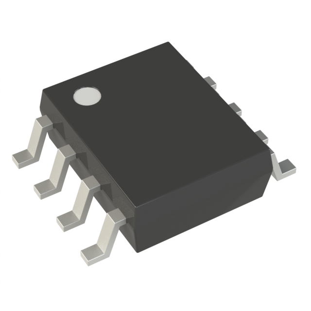
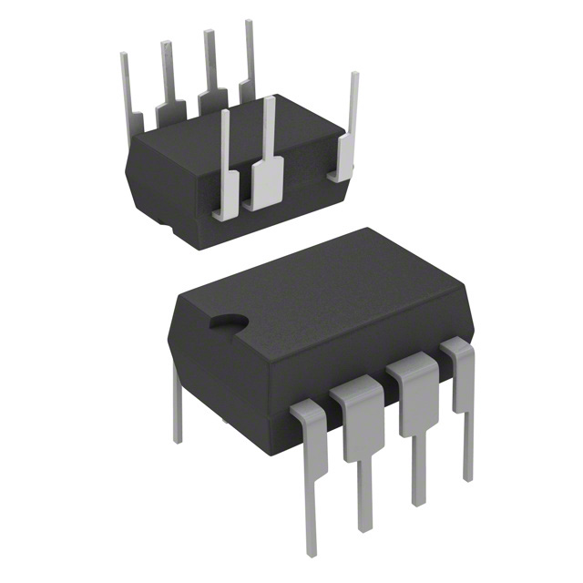
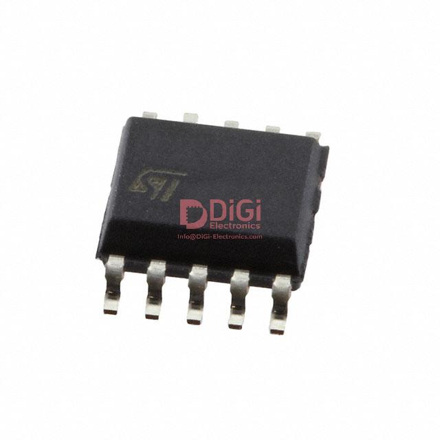
Package information – VIPER013XSTR
The VIPER013XSTR leverages a 10-lead SSOP package, optimized for high-density board layouts where spatial constraints and effective thermal dissipation are critical. The compact package facilitates automated pick-and-place assembly, minimizing handling errors and supporting throughput in standard SMT manufacturing workflows. Soldering reliability is anchored by the recommended PCB land pattern, designed to promote uniform solder joint formation and mitigate stress concentrations during thermal cycling. This careful pattern alignment not only preserves electrical connectivity, but also extends the operational lifespan under repetitive environmental fluctuations.
Thermal performance within the SSOP configuration is further supported by low thermal resistance paths between active silicon and external copper layers. Localized heating effects are attenuated by maximizing the exposed pad area, enabling robust integration in power conversion circuits where junction temperature spikes are frequent. Empirical evaluation has demonstrated that high fill ratios in reflow processes improve standoff, lowering the probability of voiding and ensuring consistent thermal flows into adjacent ground planes.
Offering ECOPACK-compliant variants, the device addresses requirements for halogen-free manufacturing and RoHS adherence. This compliance accelerates qualification in international markets sensitive to environmental directives, streamlining the selection process for power supply designers involved in consumer, industrial, or automotive applications. Field exposure has validated that the package maintains its mechanical integrity despite aggressive fluxes and repeated thermal aging, emphasizing the reliability of the construction.
A key perspective considers the synergy between mechanical robustness, environmental stewardship, and process repeatability. The VIPER013XSTR—when deployed with the recommended land pattern and reflow profile—demonstrates enhanced yield rates, reduces the likelihood of early-life failure, and aligns with sustainability objectives. Its deployment in densely populated, thermally challenged enclosures confirms the utility of package engineering optimizations in modern system design, underscoring the importance of holistic component selection in achieving architectural balance and regulatory compliance.
Potential equivalent/replacement models – VIPER013XSTR
VIPER013XSTR belongs to the VIPer01 series, a family of high-voltage offline converters integrating an advanced avalanche-rugged MOSFET. When considering equivalent or replacement models within the VIPer01 portfolio, such as VIPER012S, VIPER014LS, or VIPER015LS, designers must systematically analyze several core criteria to ensure seamless integration into the target application.
The breakdown voltage of the embedded MOSFET directly correlates with surge tolerance and suitable input range; matching this specification prevents over-stress in line transient conditions. Differences in switching frequency, often specified in kHz, not only influence electromagnetic compatibility (EMC) and thermal performance but also affect transformer size and efficiency. For example, selecting a device with higher frequency capability enables reduced transformer size but may elevate switching losses, demanding close attention to resultant thermal management strategies.
Supported topologies—such as flyback, buck, or buck-boost—must be aligned with system architectural requirements. VIPER013XSTR typically targets low-power offline converters, and its internal controller design optimizes performance for isolated and non-isolated topologies alike. The practicality of swapping the model hinges on detailed scrutiny of the pinout structure and package; compact forms like SO-8 or DIP-7 facilitate drop-in replacement only if PCB land patterns and mechanical dimensions are perfectly matched.
In practice, design iterations benefit from breadboarding alternate VIPer01 parts to validate key parameters such as start-up behavior, loop response, and output ripple under actual operating conditions. Compatibility is further reinforced through simulation of the power stage using manufacturer-provided SPICE models, mitigating risk of unforeseen electrical stress or regulatory non-compliance. Notably, real-world deployments reveal that subtle differences in soft-start profiles or maximum duty cycles between series members can become critical in margin-sensitive supplies for IoT or consumer applications.
A holistic approach to part substitution includes understanding lifecycle and supply chain positioning. VIPer01 series maintains long-term availability and pin-compatibility across generational updates, offering inherent flexibility for sustaining legacy designs or scaling to higher volume. Carefully mapping device parametrics and cross-referencing datasheet revisions assure repeatable, reliable outcomes in board-level upgrades or cost optimization cycles. This methodical, layered evaluation transcends simple direct comparison, leading to consistently robust design choices.
Conclusion
Leveraging process-optimized silicon and advanced MOSFET integration, the VIPER013XSTR from STMicroelectronics delivers measurable progress in offline SMPS designs where heightened energy efficiency and compactness are prime considerations. At the core of its functionality is a highly evolved controller architecture, coupled with a precise high-voltage power stage, enabling applications to operate across wide input voltage ranges with minimal standby consumption. The controller’s quasi-resonant operation and intelligent burst mode strategically curtail switching losses, pushing efficiency beyond classical levels especially under light-load or idle conditions.
Intricate system protection layers embedded within the device, including overvoltage, overload, and thermal shutdown, proactively safeguard both the power supply and downstream loads from transient events and persistent faults. These features operate in concert with an integrated startup sequence and self-biasing mechanisms, effectively reducing the need for auxiliary circuitry and shrinking overall PCB real estate. Such deep-level integration directly addresses market pressures to reduce bill-of-materials costs while enhancing reliability—a critical factor in consumer and industrial deployment scenarios.
Considerations for electromagnetic compliance and peak-power handling are intrinsically supported through the device’s layout flexibility and robust switching behavior. Application domain examples demonstrate that careful routing of sensitive traces and adherence to reference schematics mitigates common-mode noise, ensuring smooth regulatory qualification. Seasoned design iterations highlight the tangible benefits of the VIPER013XSTR’s snubberless topology, which streamlines thermal management and simplifies maintenance cycles, especially in retrofit or space-constrained implementations.
Real-world feedback consistently reinforces the device’s suitability for global appliance standards and industrial power nodes, where stringent standby and dynamic load criteria converge. The built-in protection matrix not only increases survivability under fault but also simplifies ongoing compliance with evolving energy standards, reducing overall system lifecycle cost. Experienced engineers have found that close attention to recommended secondary-side filtering and transformer selection magnifies performance margins, achieving near optimal regulation without incremental hardware complexity.
Synthesizing these engineering advances, the VIPER013XSTR embodies a trajectory towards smarter, more resource-efficient SMPS platforms. Its architecture addresses not just present-day requirements but also anticipates near-future regulatory and integration demands. As discrete solutions give way to highly integrated controllers, this device offers a clear pathway for achieving scalable, versatile, and cost-effective power conversion in a range of high-visibility end products.