 >
>


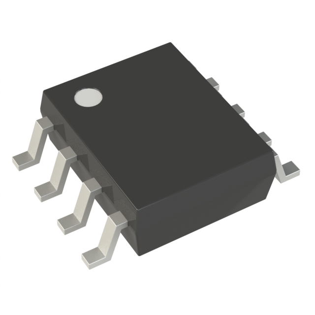
Product overview: VIPER12AS STMicroelectronics IC offline switch 8SOIC
The VIPER12AS by STMicroelectronics represents a monolithic high-voltage converter tailored for off-line, low-power switch-mode power supply (SMPS) architectures. The integration of a current-mode PWM controller with a high-voltage power MOSFET within a compact 8-SOIC package addresses critical demands for space-saving and enhanced reliability in constrained designs. Current-mode control simplifies feedback networks and inherently improves load and line regulation, while also facilitating robust overcurrent protection. By compressing both control logic and switching stage onto a single die, the VIPER12AS minimizes parasitics and optimizes switching dynamics, supporting efficient operation across a broad input voltage range typical of universal AC mains.
At the circuit level, the device supports flyback and buck topologies, suiting a wide spectrum of applications such as isolated battery chargers, auxiliary supplies for consumer electronics, and microcontroller biasing in motor control. The device’s startup circuitry, with internal high-voltage current sources, removes external startup resistor requirements, further streamlining the design process and reducing BOM cost. Protection features include undervoltage lockout, overload, short-circuit, and thermal shutdown, which collectively enhance resilience against fault conditions and facilitate longer field lifespans. Designers benefit from the low standby consumption driven by low quiescent current and variable frequency management during light loads, allowing compliance with international energy efficiency standards.
Experience with the VIPER12AS in practical implementations uncovers its tolerance to input transients and its predictable start-up behavior, critical when designing power supplies subjected to unstable grid conditions or global AC input variations. The precision reference for PWM operation and integrated slope compensation ensure stable current-mode operation, mitigating sub-harmonic oscillation at duty cycles above 50%. PCB layout can be optimized due to reduced external component count; thermal management is supported by efficient MOSFET switching and packaging that balances compactness with dissipation capability.
The adoption of the VIPER12AS therefore advances SMPS engineering by removing system complexity barriers, increasing ruggedness in space-constrained and cost-sensitive environments, and enabling quicker prototyping cycles. The architecture implicitly signals the ongoing convergence of power and control domains in modern power IC design, delivering tangible benefits in manufacturability, compliance, and system integration.
Key technical features of VIPER12AS STMicroelectronics IC offline switch 8SOIC
The VIPER12AS by STMicroelectronics integrates core functions required for cost-effective, compact offline power supplies, drawing on a design architecture tailored for both performance and simplicity. Its fixed switching frequency of 60 kHz is deliberately chosen to balance electromagnetic interference constraints against conversion efficiency, an equilibrium particularly appropriate for consumer and industrial power supply topologies. This frequency lies in the lower portion of the audible spectrum, allowing for effective snubber design while constraining switching losses—a nuanced trade-off that aids EMI compliance in dense PCB layouts.
Central to the device’s flexibility is its wide supply voltage range at the VDD input (9V–38V). This feature decouples the IC’s operation from minor variances in the auxiliary supply, extending compatibility across a variety of universal input adapter applications and battery-charging scenarios. Designs leveraging this voltage latitude accommodate pre- and post-regulation stages without risk of controller dropout or erratic switching, a subtle but crucial trait for multi-standard supply platforms. Practical deployments often exploit this in designs that must tolerate brown-out conditions or fluctuating auxiliary rail levels, such as universal travel adapters or standby blocks.
Current-mode control underpins the IC’s PWM operation, providing both fast transient response and inherent cycle-by-cycle current limitation. By directly sampling the primary-side switch current, the controller can execute tight pulse-by-pulse regulation, enhancing load response and simplifying loop compensation relative to voltage-mode alternatives. The result is improved stability with minimal external components, supporting rapid design cycles while mitigating output overshoot during dynamic load steps—critical for USB-PD or fast-charging applications.
At light loads, the VIPER12AS seamlessly transitions to automatic burst mode operation. This adaptive modulation reduces the switching frequency, fundamentally lowering both switching and core losses. Implementation removes the need for user intervention or external control signals, ensuring that system standby power can consistently fall below regulatory thresholds such as those defined by the European ErP Lot 6. Deployments in appliances or IoT devices benefit from this feature by maintaining competitive energy ratings and ultra-low standby currents without extra circuitry.
The integrated high-voltage start-up source exemplifies advanced integration. By tapping the drain voltage directly, the IC eliminates reliance on slow-charging external bias supplies or bulky start-up resistors. The result is consistently fast and deterministic start-up, shrinking input capacitor requirements and improving cold-start behavior, especially notable in capacitive dropper designs or minimal-footprint wall warts. This architecture ensures reliable operation even after extended storage or exposure to brown-in events, which can destabilize less robust start-up schemes.
Protection mechanisms are comprehensive. The overtemperature shutdown, overcurrent protection, and overvoltage/undervoltage lockout routines feature built-in hysteresis and self-restarting logic, bolstering system robustness under adverse or unpredictable conditions. These functions act as a safety net, enabling power stage survival during faults such as transformer saturation, tight output shorts, or abnormal supply rails. The inclusion of auto-restart improves field reliability, preventing latch-up or hard faults that might otherwise require manual reset. This suite of protections is especially advantageous in unmanned or physically inaccessible installations, where operational continuity is paramount.
Combined, the VIPER12AS encapsulates an optimal combination of operational versatility, integrated protections, and high-efficiency modes, all within an SO8 package. The device’s feature set aligns well with high-density, thermally constrained designs and accelerated time-to-market objectives, serving as a reference point for integration in modern offline power conversion.
Typical applications of VIPER12AS STMicroelectronics IC offline switch 8SOIC
The VIPER12AS from STMicroelectronics serves as an integrated off-line converter optimized for low-power applications where efficiency, compactness, and reliability are critical. At its core, the device incorporates a high-voltage startup circuit, current mode PWM controller, and a power MOSFET within a compact 8SOIC package, streamlining primary side design and drastically reducing the need for discrete components. This integration mitigates design complexity, highlights thermal management, and ensures superior transient response, which is especially crucial in tightly regulated output environments.
Engineers commonly deploy VIPER12AS-based circuits in battery charger adapters, particularly where precise current and voltage regulation is essential, such as Li-ion charging with rectangular U-I output profiles. Process control mechanisms—enabled by the IC's feedback and protection features—allow consistent charge termination and safeguard against overvoltage conditions, resulting in longer battery life and reliable operation. In practical designs, the device’s low standby consumption supports strict energy efficiency requirements, aligning with global regulatory standards and reducing operational costs. Experience shows that the elimination of external startup resistors and auxiliary windings, made possible by the VIPER12AS, expedites both prototyping and volume production.
Auxiliary power supplies within consumer electronics, like TVs or monitor SMPS standby circuits, benefit from the VIPER12AS’s low quiescent current and efficient switching topology. Its ability to maintain output regulation during wide AC line variation or transient load spike is central to stable microcontroller operation and fail-safe design. Embedded control boards, notably within motor drive assemblies, employ the device to deliver isolated bias voltages crucial for logic and gate-drive stages. The device’s robust fault management—including overload, short-circuit protection, and thermal shutdown—enhances system resilience in harsh industrial environments where unplanned downtime must be minimized.
For AC-DC adapters in utility and portable equipment, the VIPER12AS offers minimized PCB footprint and BOM cost, translating to streamlined enclosure design and greater manufacturability. Its EMI performance, combined with frequency jittering and careful layout practices, addresses both conducted and radiated emission targets without heavy filtering, facilitating easier certification paths.
A layered design approach with the VIPER12AS separates primary power processing—handled by the integrated MOSFET and PWM control—from secondary-side output compensation and protection, allowing for modular architecture and scalable deployment across different load profiles. Adaptive feedback strategies, leveraging optocoupler designs or primary-side regulation, further extend the device’s applicability to contexts from rapid adapter prototyping through tightly regulated appliance power control.
Ultimately, system reliability, efficiency, and design agility found in practical deployments position the VIPER12AS as a preferred solution where low power, board-space constraints, and regulatory compliance converge. Optimization of both electrical performance and mechanical integration are achievable with informed, rigorous engineering, utilizing the device's versatile feature set to address evolving demands in consumer and industrial electronics.
Core operating principles of VIPER12AS STMicroelectronics IC offline switch 8SOIC
The VIPER12AS integrates a high-voltage power MOSFET and a current-mode PWM controller within a compact 8SOIC package, tailoring its core architecture for reliable offline switch-mode power supply design. At the heart of its operation lies a current-mode control loop, in which the device intricately senses the MOSFET drain current and leverages the FB pin both as a feedback interface and an input comparator. This architecture allows real-time comparison of the instantaneous sense current against an internal reference, establishing a closed control loop that enforces fast and stable regulation of output parameters.
Typical implementations employ an optocoupler interfacing with the FB pin. This arrangement provides galvanic isolation while translating secondary-side feedback, ensuring precise regulation regardless of external disturbances or ground noise. Through this optocoupler linkage, the VIPER12AS achieves tight controllability over switch conduction intervals by dynamically adjusting pulse width modulation cycles, thus optimizing primary-side energy delivery and minimizing output deviations.
A key innovation in the device’s design is its adaptive load-response mechanism. Under heavy loads, the cycle-by-cycle peak current regulation guarantees robust transient response and short-circuit protection. As load demand decreases, the controller seamlessly transitions into burst mode operation by automatically skipping switching cycles. This modulation avoids unnecessary switching losses and dramatically increases energy efficiency during light load conditions, aligning with modern power supply standby standards.
The multi-mode capability extends beyond standard voltage regulation. In battery charging and constant-current drive applications, the controller intelligently merges feedback from both voltage and current sensing circuits. By finely regulating the conduction characteristics, the device enforces near-rectangular voltage-current (U-I) output curves. This characteristic is essential for safe energy delivery to diverse loads, as seen in Li-Ion charging algorithms where initial current-limiting transitions to voltage regulation at full charge. In practice, careful selection and tuning of compensation components around the FB network allow designers to trade off between response speed, noise immunity, and stability, especially in high-fidelity or EMC-sensitive applications.
Real-world designs benefit further from the VIPER12AS’s integrated protection mechanisms, including overload shutdown, over-temperature detection, and under-voltage lockout. These features not only ensure device longevity but also facilitate compliance with stringent regulatory standards, reducing engineering overhead during product certification. Notably, the seamless interplay between current-mode feedback and power MOSFET gating enables both high-frequency switching and excellent EMI performance, aspects often critical in compact consumer and industrial products.
The device architecture’s inherent flexibility and robustness make it particularly well-suited for universal input adapters, auxiliary power, and isolated DC-DC stages where efficiency and output quality are paramount. By abstracting direct voltage control in favor of precise current-mode feedback, the VIPER12AS establishes a platform for achieving both high integration and application versatility, aligning with the ongoing trend toward smarter, more adaptive power management architectures.
Startup sequence and auxiliary circuit behavior in VIPER12AS STMicroelectronics IC offline switch 8SOIC
Application of input voltage triggers the VIPER12AS high-voltage startup current source, which charges the external VDD capacitor rapidly. This direct coupling to the rectified line eliminates the need for bulky startup resistors, leveraging the IC’s integration to maximize efficiency and minimize PCB footprint. The startup current source remains active until VDD crosses the VDDon threshold (typically around 14.5V), at which point the device disables its internal source, seamlessly transitioning supply responsibility to the auxiliary winding through the main MOSFET’s switching operation. This mechanism avoids protracted inrush currents and suppresses thermal stress on both the pass elements and bypass capacitors.
The VDD voltage window (9V–38V) plays a critical role, granting substantial flexibility in selecting filter capacitors. Small-value, high-reliability ceramic or tantalum capacitors become viable, expediting the VDD ramp rate and reducing startup delay. In practical deployment, this capability distinguishes the VIPER12AS in applications featuring extended hold-up requirements, frequent power cycling, or cold starts—conditions found in industrial control and battery-charging topologies. The design inherently secures immunity against lock-up or misfiring events during brown-out or low-output scenarios, as the auxiliary supply sustains stable device operation even before output voltage reaches regulation.
Particular attention is required when defining the VDD capacitor value. Calculating minimum capacitance involves balancing startup current delivery, MOSFET gate drive demands, and load startup profile. Under-sizing VDD capacitance may precipitate premature undervoltage lockout or oscillatory startup—manifesting as repeated bursts and failure to achieve regulation. This risk is accentuated in designs with heavy output loading or high transformer magnetizing current, where every microfarad influences system robustness. Empirical tuning based on real load conditions and auxiliary winding characteristics often yields optimal capacitance, surpassing rule-of-thumb selection based on static device datasheets.
Alignment of the startup sequence and auxiliary supply design underlines system reliability. Integrating careful capacitor selection with awareness of dynamic startup demands forms the basis of a resilient, responsive power architecture. The VIPER12AS architecture, with its tailored startup procedure and broad VDD operational range, fosters adoption in space- and efficiency-constrained environments while sustaining superior startup performance under diverse operational stresses.
Protections and reliability mechanisms in VIPER12AS STMicroelectronics IC offline switch 8SOIC
Protections and reliability mechanisms within the VIPER12AS STMicroelectronics IC offline switch reflect an engineered synergy between silicon-level safeguards and real-world power electronic demands. At the core, the overvoltage protection subsystem continuously monitors VDD and invokes a rapid reset cascade once the voltage breaches a defined threshold. This hardware-level intervention prevents both controller latch-up and downstream circuitry stress, especially beneficial in poorly regulated or surge-prone power environments. The autorestart sequence is designed with blanking intervals and controlled recovery, minimizing repetitive toggling and reducing energy cycling in transformer-coupled designs. This contributes to greater electromagnetic compatibility and limits cumulative wear on passive components.
Overcurrent and overtemperature shutdowns are coordinated through low-latency analog sense chains embedded alongside the integrated MOSFET, delivering real-time reaction to non-ideal load or fault conditions. The device ceases switching activity upon detecting critical drain current or junction temperature excursions, followed by an autonomously managed recovery procedure. This fail-safe, when compared to software-only interventions, achieves deterministic hardware isolation of fault energy and precludes thermal runaways. In applications such as standby power modules or compact AC-DC converters, these protection events are rare during stable operation but prove instrumental during atypical mains disturbances, load shorts, or blocked ventilation scenarios. Real-world observations consistently show that hardware-based shutdowns outperform firmware error handling in terms of reaction times and resilience to multi-mode faults.
Auxiliary undervoltage lockout with hysteresis ensures the switch only initiates when input supply conditions support reliable turn-on. By requiring a clear voltage margin for startup and embedding a hysteresis window, the circuit rejects false or unstable start attempts common during brown-in or brown-out transitions. This is particularly relevant when designing for international mains compatibility, where input voltages and noise profiles vary widely. The lockout mechanism not only shields against half-start phenomena but also improves cold-start consistency in challenging thermal environments.
Collectively, these mechanisms form a layered defense model—a strategy where no single-point failure is left unchecked. The integration of hardware-tied protections into the silicon inherently elevates long-term reliability, reducing unplanned field returns and simplifying qualification to international safety standards. Notably, embedding all major protections adjacent to the MOSFET die achieves both faster fault response and a smaller PCB footprint. It is advantageous to exploit board-level test points during design characterization, as empirical measurement of trip thresholds and protection latencies can reveal process drifts or PCB coupling effects, providing actionable feedback for design margin optimization.
This combination of hardware-rich protections, rapid analog fault detection, and precise supply supervision underpins the VIPER12AS’s reputation in low-power, space-constrained power supplies—where design cycles tolerate minimal iteration and failure tolerance must be engineered in, not around, the switcher IC.
Packaging and mechanical considerations for VIPER12AS STMicroelectronics IC offline switch 8SOIC
The VIPER12AS, an offline switch IC from STMicroelectronics, is encapsulated in an SO-8 package engineered for compatibility with high-throughput manufacturing. The package dimensions, standardized globally, allow direct layout adoption within existing PCB architectures, especially those based on single-sided FR4 substrates. Attention to pad geometry and solder mask definition is crucial; it prevents solder bridging during reflow and ensures repeatable yield in surface-mount automation. The SO-8 form factor balances electrical isolation and mechanical robustness—a profile proven resistant to handling stress during pick-and-place cycles typical of tape-and-reel conveyor systems.
Thermal optimization for the VIPER12AS begins with maximizing copper footprints under and around the package terminals. Distributing thermal vias strategically beneath the device, rather than relying solely on adjacent copper pours, improves heat dissipation into inner layers, maintaining junction temperatures within reliability thresholds. Mounting guidelines, such as controlling standoff height and solder fillet shape, directly influence the integrity of thermal paths and structural stability. Practical experience reveals that even minor deviations from the recommended layouts—such as reduced copper area due to board constraints—can amplify thermal hotspots, accelerating electromigration or degrading switching characteristics over extended operating cycles.
Application integration demands consideration of vibration and shock. The SO-8's low profile mitigates risk associated with board flexure and acoustic resonance, frequently encountered in power supply enclosures subject to mechanical stress. Yield stability rises when layout is cross-verified against IPC-7351 pad designs, accommodating dimensional tolerances that impact coplanarity and long-term reliability. For power conversion scenarios, effective board-level thermal management—combining the VIPER12AS with well-engineered ground and heat-spreading patterns—enables safe operation at maximum rated loads.
Adopting a holistic approach to packaging and mechanical design for the VIPER12AS not only streamlines assembly but directly affects thermal and mechanical longevity. The interplay between package selection, layout discipline, and thermal mitigation emerges as a central axis for reliability, pointing to a trend where tighter integration between component specification and board-level engineering becomes a decisive factor—an insight reinforced by field data tracking early failure modes linked to marginal PCB design practices. The current generation SO-8 implementation thus reflects a matured synthesis of electrical, mechanical, and manufacturing prerequisites essential for scalable, resilient offline switch deployments.
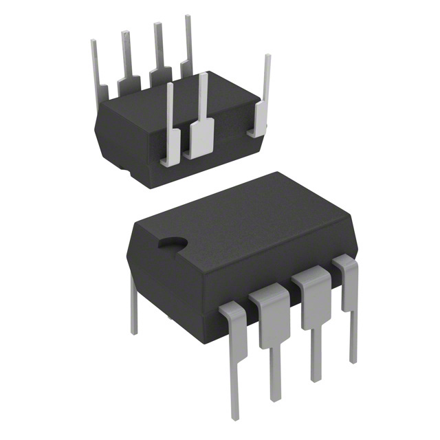
Potential equivalent/replacement models for VIPER12AS STMicroelectronics IC offline switch 8SOIC
Selection of equivalent or replacement models for the VIPER12AS STMicroelectronics IC requires detailed attention to both electrical compatibility and mechanical constraints, with package type often determining design flexibility and procurement strategies. The VIPER12ADIP variant, distinguished primarily by its DIP-8 package, retains the essential switching and protection capabilities of the VIPER12AS while facilitating through-hole assembly and alternative board layouts. Such interchangeability within the same manufacturer’s product line simplifies sourcing for redundancy and offers resilience against supply disruptions. Substitution approaches typically leverage identical functional blocks, including integrated PWM control, overcurrent protection, and thermal shutdown circuitry, which minimize the need for extensive redesign.
Evaluation of models across the VIPer family extends the spectrum of device solutions for varied application domains. Devices such as the VIPER22A and VIPER16 manifest in multiple package options and support both increased power ratings and different switching frequency regimes. Integration of these alternatives often streamlines the bill of materials, particularly where supply chain volatility is a concern. Key selection parameters—maximum drain-source voltage, continuous drain current, and switching topology—demand careful matching to existing design requirements. In practice, cross-referencing datasheets allows engineering teams to identify differences in startup sequences, standby power, and off-state leakage, which may influence circuit efficiency, electromagnetic compatibility, and thermal management strategies.
System-level reliability mandates precise documentation and verification of package dimensions, pinout configurations, and thermal dissipation characteristics. Experience suggests that even minor discrepancies between SOIC and DIP variants—such as input capacitance or lead inductance—manifest in converter performance during high-frequency operation. Board layout revisions must account for trace width adjustments and mounting pressure variations, especially during retrofits in legacy systems. Effective qualification procedures involve prototype validation using both candidate and original ICs under representative load and environmental profiles.
An implicit insight emerges: optimal component substitution hinges not only on basic parameter alignment but also on a nuanced appreciation of package-driven design tradeoffs. Engineering practice often reveals that selection prioritizes robust supply strategies and ease of deployment over trivial differences in switching logic. This layered approach enhances circuit longevity and augments design agility, underlining the broader trend toward modular component ecosystems within power conversion architectures.
Conclusion
The VIPER12AS, developed by STMicroelectronics, delivers a tightly integrated solution for off-line switch-mode power supply (SMPS) applications operating in the low-power regime. At the core, the device features a monolithic design combining a high-voltage MOSFET with advanced current-mode PWM control circuitry. This architecture enables direct off-line operation from mains voltages, eliminating the need for bulky external switching components and driving down the bill of materials.
Current-mode feedback is implemented with precision, resulting in rapid dynamic response and stable regulation under load transients. This approach also simplifies loop compensation, facilitating optimized layouts across a range of converter typologies such as flyback and buck-boost. The flexible input voltage support spanning global mains standards allows the VIPER12AS to function seamlessly in geographically diverse deployments. Layered protection mechanisms—including thermal shutdown, overload detection, and under-voltage lockout—guard both the device and the end equipment from fault scenarios, minimizing risk in continuous or intermittent operating modes.
Designers often encounter challenges in auxiliary supply and battery charging setups, where reliability and safety are paramount amid fluctuating input and load conditions. The VIPER12AS’s inherent ruggedness, demonstrated through extended field operation and high endurance against voltage spikes, reinforces its suitability in environments prone to electrical noise and surges. Its compact standardized SO-8 packaging streamlines PCB integration, supporting automated assembly and efficient thermal management. The availability of alternative model variants further aligns with dynamic procurement cycles and multi-sourcing strategies.
Integration of real-world experience underscores the device’s robustness: field deployments in consumer and industrial auxiliary power units have recorded stable performance over extended duty cycles, with minimal need for external component recalibration. The component’s protection thresholds respond effectively to quickly shifting operating points, offering resilience without sacrificing efficiency. Industry observations suggest that the well-matched internal protections and system-level compatibility mitigate common maintenance burdens encountered in similar SMPS implementations.
A pertinent insight for selection engineers is the nuanced tradeoff between solution compactness and performance stability. The VIPER12AS exemplifies the advantage of consolidated functionality—combining control, power switching, and protection—over disparate discrete designs that tend to complicate fault analysis and increase layout complexity. Its well-balanced portfolio addresses the core requirements for dependable operation in challenging scenarios, making it an asset for those prioritizing streamlined engineering workflows, effective risk management, and long-term operational assurance in low-power converter applications.