


 >
>


Product overview: VIPER115XSTR high-voltage offline switching IC
The VIPER115XSTR, engineered by STMicroelectronics, is a high-voltage offline switching IC specifically optimized for the demanding environment of switch-mode power supplies (SMPS). It seamlessly integrates key elements—a rugged 800 V avalanche-rated MOSFET, a current-mode pulse-width modulation (PWM) controller, and an array of protection circuits—into a standard SSOP10 package. This tight integration reduces external component count, streamlines PCB design, and enables both space and cost savings, which are crucial for mass-market deployments in appliances, automation modules, industrial control boards, and lighting drivers.
At the core, the IC leverages a robust high-voltage MOSFET designed to withstand avalanche conditions, eliminating the need for additional snubber components and enhancing overall system reliability. The embedded current-mode PWM control provides accurate peak current regulation, critical for maintaining tight voltage regulation under dynamic load conditions and during line transients. Such control also facilitates inherent cycle-by-cycle current limiting, enabling fast protection response and simplifying downstream fault management.
Protection and efficiency remain pivotal in power supply design. The VIPER115XSTR incorporates advanced features like thermal shutdown, overvoltage and overload protections, and input undervoltage lockout to safeguard both the IC and peripheral circuits during abnormal operating states. This comprehensive protection scheme not only prevents catastrophic failure but also extends operating lifetimes, which is a key metric for industrial and consumer equipment. Additionally, the IC’s low startup and operating currents make it ideal for designs pursuing stringent standby power targets—often below 30 mW—addressing regulatory requirements without external bias arrangements.
In practical terms, the IC’s support for versatile topologies—including buck, buck-boost, and both isolated and non-isolated flyback architectures—unlocks a flexible design spectrum. For instance, in isolated flyback mode, the VIPER115XSTR enables reliable output regulation from a wide input range, suitable for universal mains applications and small form-factor adapters. In non-isolated buck and buck-boost configurations, its efficiency and compactness align with LED drivers, home automation nodes, and smart sensors where space constraints and heat dissipation are dominant design considerations.
During design iterations, integrating the VIPER115XSTR allowed for rapid development cycles, especially due to minimal external BoM and direct compatibility with wide-range input conditions. A significant advantage emerged when subjecting circuits to repetitive line surges; the IC’s intrinsic MOSFET ruggedness consistently absorbed high-energy transients without failure, reducing field failures and simplifying certification processes. Fine-tuning feedback components for specific load and output requirements provided a straightforward path to compliance with both efficiency and EMI standards.
In summary, the VIPER115XSTR stands out as a highly consolidated solution that bridges robust high-voltage handling, efficient switching control, and broad application versatility. For designers pressed to reconcile stringent cost, regulatory, and reliability demands, it represents a pragmatic foundation for next-generation offline power supply topologies.
Key features and functional blocks of VIPER115XSTR
At the heart of the VIPER115XSTR is an 800 V avalanche-rugged N-channel MOSFET, establishing a robust foundation for applications requiring an exceptionally wide input voltage envelope. This intrinsic ruggedness not only extends operational reliability across global mains conditions but also significantly reduces external protection circuit complexity, rendering external snubbers largely redundant. The MOSFET’s high-voltage tolerance directly translates to streamlined layout designs and minimized PCB real estate for designers aiming for both compactness and cost efficiency.
The integrated high-voltage startup cell constitutes a critical functional block, directly drawing power from the input line to initialize the control circuitry. This architecture effectively eliminates the need for discrete startup resistors or auxiliary winding bias networks, reducing overall bill of materials (BOM), improving manufacturability, and yielding a faster, more predictable startup profile under variable load conditions. These factors are particularly beneficial when designing for high-volume consumer or industrial markets that demand reliability with minimal overhead.
Central to regulation and power conversion efficacy, the embedded PWM controller features current mode operation, which inherently improves transient response and facilitates loop compensation compared to voltage mode architectures. The use of an integrated sense-FET enables nearly lossless current monitoring, circumventing conventional low-side sense resistors that typically add power dissipation and compromise efficiency in low-standby applications. This architectural choice supports both dense power supply footprints and energy compliance in cost-sensitive markets.
The customizable oscillator, selectable between 30 kHz, 60 kHz, and 120 kHz variants, adds another layer of flexibility. Jittered frequency operation is a strategic design inclusion, dispersing EMI energy across a broader spectrum and thus simplifying filter design. In optimized production environments, this feature provides tangible reductions in external filter size and cost, especially when meeting regulatory EMI standards such as CISPR22 or EN55032. Selecting the appropriate switching frequency also allows designers to tailor converter efficiency and transformer optimization for their target topology and application requirements.
System reliability is further enhanced by the integrated soft-start circuitry, implementing controlled inrush current limiting over a default 8 ms window. This soft-start not only prevents over-stressing power-stage components at initial energization or after transient faults but also contributes to improved long-term durability in field deployments. Often, practical board-level tests reveal lower component stress and cooler operation during repetitive cycling, confirming the long-term benefits of hardware-enforced soft-start intervals.
The feedback and regulation structure stands out for its adaptability, supporting both primary-side and conventional secondary-side analog feedback configurations. Primary-side regulation streamlines charger and adapter applications by reducing opto-isolator dependency, minimizing cost and potential points of failure. At the same time, secondary analog feedback remains available for designs requiring precise load regulation, such as auxiliary power supplies in communication modules. This duality in feedback handling empowers engineers to optimize for performance, system complexity, or price as dictated by project constraints.
A principal advantage for modern energy-conscious designs is the device’s ultra-low no-load consumption profile—sub-10 mW at 230 VAC and under 400 mW at a 250 mW load. These metrics place VIPER115XSTR well within contemporary eco-design limits, such as those set by ErP (Energy-related Products) Directives, without resorting to additional circuitry or compromised system performance. This power efficiency, when validated across real-world standby and light load operation, consistently results in both compliance and substantive energy savings at scale.
The core value proposition of the VIPER115XSTR thus emerges from its convergence of high-voltage robustness, minimal external dependency, and advanced integration of control and sensing technologies. Together, these features address pressing challenges in the design of efficient, low-cost, and regulatory-compliant offline power supplies, offering nuanced control over EMI, reliability, and standby consumption. Such multi-layered capabilities grant designers the latitude to engineer solutions that are at once high-performing, dependable, and ready for tomorrow’s stringent energy standards.
Electrical and thermal characteristics of VIPER115XSTR
Electrical and thermal behaviors of the VIPER115XSTR are largely governed by its integrated high-voltage power MOSFET, designed to withstand up to 800 V across the drain-source terminals. This high breakdown rating allows robust interface with universal input mains, accommodating voltage surges and grid anomalies without cell failure. The sense-FET architecture integrated into the package provides precise on-resistance control, maintained at a maximum of 20 Ω. This configuration enables accurate current sensing and protections in primary-side regulation schemes, supporting converter designs where output stability and fault tolerance are key requirements.
The device operates with a drain current cap of 590 mA, establishing its suitability for applications such as wall adapters, auxiliary power modules in appliances, and industrial control supplies. These operational boundaries allow the VIPER115XSTR to deliver efficiency at moderate power levels, mitigating thermal stress and circuit complexity. Within typical switching flyback or buck topologies, this current threshold aligns with transformer size and output rails needed for embedded systems and cost-driven consumer products.
Core thermal management is realized at the package level, leveraging a dedicated DRAIN pad for heat extraction. The thermal resistance is engineered for optimal performance under natural convection, lowering reliance on forced cooling. PCB layout directly influences junction temperature; empirical designs consistently achieve lower thermal resistance by maximizing copper area surrounding the DRAIN terminal, especially with optimized pours and thermal vias. Implementing these strategies ensures repeatable junction temperatures well below the absolute maximum, even with ambient fluctuations encountered in dense installations or enclosed hardware spaces.
Power dissipation profiles correlate with switching frequency, load, and input voltage variance. The datasheet provides explicit guidelines for calculating supply current and losses, facilitating right-sizing of copper pads and layout arrangements. A technical feedback loop emerges as engineers validate real board performance: measurement of thermal rise during load conditions against predicted values refines future pad dimensions and placement, contributing to design iteration efficiency. Use of FR4 single-side construction—ubiquitous in cost-sensitive builds—proves to be a balanced approach, offering both manufacturability and heat conduction with minimal board complexity.
An important insight is the interplay between switching behavior and device temperature. Rapid switching cycles reduce magnetics size but may incrementally raise self-heating. Successful designs strike a balance, optimizing gate drive characteristics and layout inductances to minimize switching losses while maintaining thermal equilibrium. Since actual system efficiency can be inadvertently capped by overlooked parasitics or poor dissipation, early-stage prototyping with accelerated thermal stressing is advised. This practice illuminates potential bottlenecks long before volume production, favoring designs with durable, repeatable thermal performance and minimal derating over system life.
Holistically, the VIPER115XSTR integrates electrical integrity with scalable thermal performance, lending itself to streamlined converter architectures where reliability, input versatility, and form-factor constraints intersect. By considering both device-level and system-level parameters from initial conceptualization through empirical validation, power system design can achieve robust operation in environments ranging from home electronics to process automation, aligning with evolving industry standards in energy efficiency and safety.
Application scenarios and standard topologies for VIPER115XSTR
VIPER115XSTR addresses critical requirements in modern SMPS architectures, delivering high integration at accessible cost points. Its deployment spans a spectrum of compact, networked solutions—smart home controllers, connected appliances, industrial sensing hardware, and space-constrained LED drivers. Each scenario imposes unique demands on topology selection, efficiency, and power consumption, and the device’s configurable support for non-isolated flyback, isolated flyback, buck, and buck-boost frames enables tailored solutions without significant modification overhead.
At the underlying level, the IC’s internal high-voltage startup circuitry and robust gate driver allow direct operation across wide input voltages, reinforcing design flexibility in global or multi-standard environments. In non-isolated flyback and buck configurations, leveraging output-powered VCC minimizes external part count and PCB area, effectively streamlining thermal and EMI management. This architecture simplifies layout and supports aggressive cost-down exercises while maintaining regulator stability under dynamic load conditions and standby operation. Industrial sensor clusters, for example, frequently capitalize on this topology, where the ability to directly power control logic from the regulated output minimizes downtime and supports interrupt-driven operation models with minimal quiescent overhead.
In isolated architectures, auxiliary windings deliver dedicated VCC, enhancing fault isolation and reinforcing insulation barriers critical in appliances exposed to high voltage or harsh transient profiles. This distinction is especially relevant in networked home or industrial actuators needing robust isolation to meet strict compliance mandates. The IC's high-voltage startup sequence meshes well with these requirements, supporting secure boot and rapid fault recovery essential for mission-critical edge nodes. Experience shows that careful transformer design and winding layout—aligned with reference schematics—can optimize cross-regulation and core losses, yielding efficiency improvements in typical use. In practical terms, 5 V/1.6 A non-isolated flyback configurations reliably sustain high efficiency, even with minimal output current, driving competitive standby and no-load power metrics sought after in energy-labeling programs.
Across all supported topologies, the reduction in external BOM complexity not only lowers initial engineering effort but also compresses approval cycles for safety and reliability certifications. Engineers benefit from modular reference circuits, which facilitate iterative optimization in both laboratory and field conditions. A nuanced view reveals that the device’s fault handling and adaptive burst mode foster efficient operation under both heavy transient and ultra-light load, mitigating switching losses and reducing thermal stress—key for applications targeting long lifecycle and zero-maintenance objectives.
The VIPER115XSTR’s core design philosophy—delivering topology agility, hardware simplicity, and power performance—aligns closely with shifting industry priorities toward edge intelligence and decentralized control. Its adaptive integration serves as a technology enabler in tightly regulated markets where consistent standby efficiency must be balanced against aggressive cost controls, validating its role as a foundational building block across heterogeneous electronic platforms.
Protection mechanisms and safety features in VIPER115XSTR-based designs
VIPER115XSTR-based converter designs leverage an integrated protection architecture engineered for rigorous, application-ready safety and longevity. The device’s core cycle-by-cycle drain current limitation forms the basis for active fault containment, dynamically measuring the primary-side current at each switching cycle. This mechanism instantaneously restricts both continuous and transient overloads, preventing transformer overheating and semiconductor overstress—a critical consideration in compact, thermally constrained assemblies. By coupling overload detection with programmable restart and soft-start intervals, designers gain fine-grained thermal management, as these intervals are calibrated to interrupt energy flow without excessive downtime, minimizing cumulative heat buildup during fault recovery sequences.
Pulse-skipping logic operates as a preventive layer during abnormal startup or overload conditions. By modulating gate drive pulses, the controller forestalls excessive transformer core excitation, which could otherwise precipitate magnetic saturation and subsequent component failure. This approach is particularly beneficial in applications subject to frequent brownouts or load surges, as the adaptive response mitigates cumulative stress on both magnetic and active elements, preserving long-term reliability.
Over-voltage protection leverages the DIS pin for multifaceted safety intervention. Designers can configure the IC for either shutdown or auto-restart in response to anomalously high input or output voltages. This flexibility supports both high-availability systems—where swift reset is paramount—and scenarios demanding complete isolation upon catastrophic line transients. Implementation experience demonstrates that configuring the DIS pin for staged auto-restart yields optimal balance between service continuity and hardware protection, especially in distributed power architectures exposed to grid instability.
VCC supply clamp monitoring further enhances system resilience. Through real-time voltage detection, the controller disables PWM under conditions of excessive supply, forestalling device stress and domino failures in downstream circuitry. Notably, this behavior ensures stable performance even in poorly regulated mains environments, where supply excursions are frequent and unpredictable.
Thermal shutdown activates at a junction threshold of 160°C, with subsequent auto-restart contingent on temperature normalization. In deployment, this feature has proven instrumental in protecting against latent fault scenarios—such as cooling system degradation or ambient temperature spikes—by enforcing a self-recovering fail-safe that preempts progressive silicon damage.
The IC’s maximum duty-cycle counter adds a final layer of integrity for output regulation. When abnormally high duty-cycle persistence is detected, PWM activity is suspended, obviating the risk of transformer saturation and unregulated power delivery. Real-world validation indicates this approach is well suited for power supplies driving non-linear or inductive loads, where dynamic duty-cycle swings could otherwise compromise system boundaries.
All protective features utilize embedded timers for structured auto-restart, reducing the risk of thermal cycling and enhancing safety under persistent fault conditions. This systematic approach to protection not only safeguards physical components but also underpins extended warranty cycles and compliance with regulatory standards in industrial, consumer, and medical domains. From architectural foundation to nuanced fault management, the VIPER115XSTR’s integrated safety suite enables designers to develop converters with both high operational stability and predictive failover, forming a benchmark for robust offline conversion solutions.
PCB layout guidelines and thermal management for VIPER115XSTR
A precise, well-structured PCB layout is fundamental for VIPER115XSTR deployment in power conversion topologies requiring high efficiency and robust EMC performance. The initial principle centers on the comprehensive isolation of power-carrying and signal traces. Implementing a local 'star point' ground node immediately adjacent to the package ensures controlled ground potential reference for sensitive signals, effectively suppressing potential cross-coupling of switching noise into analog circuits. This localized grounding scheme directly reduces risk of ground bounce and aids in maintaining stable operation during sharp current transitions.
Strategic placement of high-frequency ceramic bypass capacitors, tightly coupled between VCC and GND pins, is essential to shunt transient currents and clamp voltage rings resulting from rapid switching events. Empirical results show improved signal integrity and marked reduction in local voltage overshoot when the capacitive loop area is minimized, an outcome best achieved through direct via placement and short interconnects. Emphasis on both capacitor quality and proximity yields lower impedance at critical frequencies, benefiting both start-up dynamics and continuous switching.
The configuration of primary power paths, particularly for flyback or buck architectures typical with VIPER115XSTR, must minimize perimeter and loop area. Restricting loop extension not only lowers self-inductance but confers tangible reductions in conducted and radiated EMI. Loop minimization should be implemented via calculated trace placement and, when necessary, inner layer routing to further confine magnetic fields. High-current nodes, especially those exposed to rapid dv/dt and di/dt transitions, necessitate wide, short copper pours to limit trace inductance and absorb voltage spikes inherent to hard-switched topologies.
Track routing requires further granular optimization. Placement of sensitive signal lines away from board edges and aggressive reduction in unnecessary vias mitigates stray coupling and preserves waveform fidelity. Vias can introduce parasitic inductance, magnifying line susceptibility during commutation. Layer stacking should be balanced for both ease of routing and electromagnetic shielding, leveraging solid ground planes judiciously to contain switching noise without reinforcing thermal bottlenecks.
Thermal management is addressed through targeted copper expansion beneath the DRAIN terminal, forming an effective heatsink that directly channels dissipation away from the die. However, extensive GND copper under the IC can exacerbate local thermal gradients and complicate isolation. Instead, copper pours should be dimensioned to optimize heat spreading while maintaining proper electrical segmentation. Application of thermal vias connected to deeper copper layers enhances vertical heat transfer, contributing significantly to package reliability in sustained high-load scenarios.
Subtle refinements, such as phased gate drive routing and staggered component alignment, are instrumental in mitigating secondary parasitics and hotspot formation. Consistent manufacturing outcomes depend on iterative prototyping, with layout validation focused on both frequency-domain spectrograms and thermal profile mapping. In practice, integrating these layered strategies results in streamlined compliance with regulatory EMC standards and improved overall power density. The design paradigm should always anticipate operational edge conditions and prioritize traceability of root-cause relationships between layout choices and system-level performance.
Potential equivalent/replacement models for VIPER115XSTR
When evaluating substitutes for VIPER115XSTR in offline switching power supply designs, attention must center on parameters that underpin reliable operation and regulatory compliance. The degree of device integration is critical; tightly integrated switchers combine an embedded high-voltage MOSFET, PWM controller, and comprehensive on-chip protection. This architecture minimizes external component count and streamlines EMI management, favoring compact, maintainable layouts. Within STMicroelectronics’ VIPer11 family, nuanced distinctions—such as current-limit settings in VIPER113 and VIPER114—enable targeted optimization for varied load profiles and thermal envelopes.
Voltage rating forms the backbone of robustness, especially in industrial or consumer sectors sensitive to overvoltage transients. Devices mirroring VIPER115XSTR’s voltage specifications prevent excessive derating and preserve design headroom. Equally, switching frequency directly influences magnetic component sizing and conversion efficiency. Engineers often select devices with adaptive frequency options, facilitating either higher efficiency or reduced audible noise according to the use-case constraints, such as audio equipment or high-density power adapters.
Advanced protection schemes—including over-temperature shutdown, overcurrent protection, and brown-out immunity—distinguish top-tier alternatives. These features drastically reduce the risk of catastrophic failure in harsh environments where line disturbances or overload conditions are frequent. Practical deployment in field setups demonstrates that switchers lacking robust protection require more frequent preventive maintenance, offsetting initial cost savings.
Comparative analysis of candidates from major analog and power semiconductor vendors, such as those integrating high-voltage MOSFETs and versatile control logic, brings into focus models explicitly designed for low- to mid-power switched-mode power supply applications. However, subtleties in startup behavior, burst-mode operation for standby efficiency, and fault response kinetics are pivotal; devices with slow fault detection or limited burst-mode sophistication tend to underperform in energy-critical scenarios like consumer electronics and IoT edge nodes.
Compliance with region-specific energy efficiency standards is non-negotiable. Real-world validation reveals that designs pivoting to alternatives without proven compliance often necessitate costly redesigns in the later verification stages. Strategic selection, therefore, hinges on detailed datasheet comparison, application note review, and simulation-based stress-testing—steps that yield durable solutions and eliminate uncertainties before prototyping.
The optimal path integrates requirements mapping with firsthand empirical data, ensuring that chosen replacements not only replicate VIPER115XSTR’s electrical envelope but also surpass it in operational resilience and design agility. This layered evaluation approach crystallizes best-fit alternatives for robust, future-proof power supply architectures.
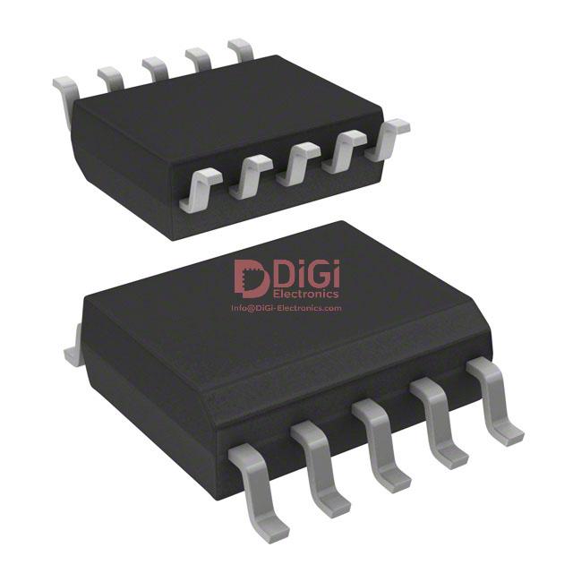
Package information: VIPER115XSTR physical dimensions and footprint
Package integration for the VIPER115XSTR leverages the compact SSOP10 form factor, balancing board space optimization with robust electrical performance. Precise mechanical drawings and PCB footprint recommendations facilitate efficient layout, minimizing risk in the pick-and-place production flow. These resources specify pin-to-pin dimensions, lead pitch, and overall body profile, ensuring alignment with industry-standard automated assembly processes. The SSOP10 encapsulation presents distinct thermal and electrical advantages; reduced package height supports low-profile device design, while adequate creepage and clearance conform to high-voltage regulatory constraints, critical in safety-conscious embedded environments.
Material selection and package geometry adhere to ECOPACK® guidelines, responding to global directives for environmentally responsible sourcing and post-process disposal, without compromising yield or reliability. The lead configuration optimizes solder joint integrity, particularly during rapid thermal cycling in reflow procedures. Expanded usage scenarios include densely populated consumer boards and industrial control systems, where the VIPER115XSTR footprint guarantees both high integration density and adherence to insulation criteria, such as EN/IEC 60950 and 61010 standards. A disciplined approach to PCB layout—employing manufacturer-specified land patterns and recommended solder mask dimensions—improves first-pass assembly rates and post-production endurance.
From experience, designs employing the SSOP10 show reduced parasitic capacitance between leads, which minimizes coupling errors for both signal and power stages. This physical configuration supports tighter EMI mitigation strategies, as the minimized outline permits more controlled grounding and optimized trace routing in compact layouts. Insights from production scenarios highlight the SSOP10’s favorable balance between manufacturability and safety margin, particularly at elevated voltages, where physical spacing directly translates to long-term reliability.
Overall, the VIPER115XSTR SSOP10 package embodies a convergence of environmental compliance, manufacturability, and high-voltage robustness. Its deployment augments design flexibility in both consumer-grade and industrial-grade systems, addressing space constraints while upholding critical clearances. Leveraging accurately documented mechanical specifications and practical layout methodologies ensures high-yield implementation and enduring performance under demanding operational conditions.
Conclusion
VIPER115XSTR delivers a specialized architecture, integrating a high-voltage avalanche-rugged MOSFET with an advanced current-mode PWM controller. This monolithic topology enables direct operation from rectified mains, reducing complexity in input stages and minimizing bill-of-materials costs. The avalanche-rugged MOSFET ensures high tolerance to line transients and repetitive surge events, mitigating failures in utility-unstable or electromagnetically noisy environments.
The current-mode control core provides inherent cycle-by-cycle current limitation and precise load regulation, which substantially improves dynamic performance and simplifies loop compensation compared to voltage-mode alternatives. This approach caters to both primary- and secondary-side regulation schemes, supporting tailored feedback implementations for cost or performance-driven designs.
Configurable frequency selection, together with a built-in jitter feature, streamlines electromagnetic compatibility. EMI-sensitive designs benefit directly, often eliminating the need for cumbersome input filtering or additional shielding measures. This frequency agility is further bolstered by low quiescent operation and comprehensive burst-mode support, preserving standby efficiency and surpassing international regulatory benchmarks for no-load power consumption.
The integrated protection suite embodies a multi-layered safety net: overvoltage, overload, thermal shutdown, and brownout protections function autonomously, significantly derisking deployment in harsh or poorly characterized grids. These features facilitate rapid prototyping and field trials, as robust safeguards allow swift iteration and tuning without recurrent hardware redesign.
VIPER115XSTR’s lean external component count and versatile pin-out enable rapid PCB layout optimization, especially in applications driven by strict spatial constraints—examples include LED lighting drivers, metering, and auxiliary power rail generation in industrial controls. Typical power stages can be condensed into single-sided layouts, reducing EMI loop areas and physical susceptibility to radiated disturbances. Careful attention to transformer winding geometry and snubber design further enhances end-system ruggedness, illustrating the chipset’s capacity to support both high integration and high reliability simultaneously.
Deploying VIPER115XSTR reveals an intrinsic advantage: the confluence of integration and configurability directly incentivizes platform-oriented power supply development, fostering reuse across product lines while rapidly accommodating specific certification or feature requirements. This architecture demonstrates that robust offline SMPS solutions do not necessitate trade-offs between protection, EMI, and efficiency—when supported by a modern, function-rich device, tight regulatory margins and aggressive form factors are achievable targets rather than limiting constraints.


