


 >
>


Product overview of VIPER06LN STMicroelectronics
The VIPER06LN from STMicroelectronics integrates advanced power conversion and control technology within a single compact IC, enabling the development of cost-effective, robust, and highly efficient offline power supplies. At its core, the device combines a current-mode PWM controller and a high-voltage avalanche-rugged MOSFET, supporting direct interface with rectified mains. This architecture eliminates the requirement for an auxiliary bias winding in low-power scenarios, substantially streamlining both schematic and PCB layouts.
Focusing on energy efficiency and regulatory compliance, the VIPER06LN addresses key challenges in modern power management. Its low-power startup and ultra-low standby consumption—enabled by its integrated control and power functions—directly contribute to meeting stringent standby and eco-design criteria such as those set by the EU ErP Directive. The absence of auxiliary winding not only reduces external component count, lowering BOM and assembly costs, but also enhances long-term reliability by limiting failure points and simplifying thermal management.
The device is housed in a standard 7-DIP package tailored for high-voltage robustness. Its lead pitch and internal spacing facilitate creepage and clearance distances up to 800 V, which is critical in equipment requiring safe isolation from electrical overstress. This packaging also fits well into existing through-hole manufacturing setups or hybrid THT/SMT boards.
Versatility is embedded in the VIPER06LN’s support for both buck and flyback topologies. Designers gain flexibility in serving a range of low-power applications—such as auxiliary supplies in home appliances, industrial controls, or standby power converters for consumer devices—by selecting the most appropriate topology for efficiency, output regulation, and design constraints. The integrated MOSFET’s avalanche ruggedness offers margin against line surges and overloads, a frequent real-world pain point in harsh grid environments or locations subject to significant transient voltages.
Reliable startup, low EMI emissions through frequency jittering, and embedded protection features—including overload, overtemperature, and short-circuit protection—extend the device’s suitability to demanding environments. Specific board-level practices, such as careful PCB trace separation and decoupling, further leverage the device’s high-voltage credentials and inherent EMI optimization to deliver quiet, robust operation even in densely populated enclosures.
An important insight is the impact of integration on development time and qualification. By collapsing functions into a monolithic device, the VIPER06LN accelerates prototyping, reduces sourcing complexity, and minimizes failure analysis in field returns. This approach is particularly valuable for organizations optimizing for rapid design cycles or scaling production across multiple small-wattage platforms.
Experienced designers often find added benefit in the device’s rapid fault response and consistent startup performance under varying input conditions. Optimization of snubber networks and thermal pathways, although simplified by integration, remains essential for maximizing both lifetime and performance in demanding use cases.
The VIPER06LN exemplifies the strategic convergence of regulatory compliance, system integration, and practical engineering, making it a cornerstone choice for engineers seeking high-reliability, compact AC-DC conversion without the overhead of legacy discrete approaches.
Applications of VIPER06LN STMicroelectronics
The VIPER06LN from STMicroelectronics demonstrates robust adaptability across diverse power conversion scenarios, owing to its integrated high-voltage startup circuitry, advanced PWM controller, and compact package. At the core, its architecture enables direct connection to the mains supply, eliminating the need for bulk external components common in traditional capacitive dropper designs. This not only minimizes PCB footprint but also increases system reliability—particularly in consumer electronics where board space and long-term durability are paramount.
Within home appliance power modules, the device streamlines power stage design by integrating protection features such as overload, short-circuit, and thermal shutdown. These mechanisms intrinsically support compliance with global safety and electromagnetic compatibility standards, crucial for household equipment deployed in widely varying grid environments. The device’s capability for efficient standby operation further drives down energy consumption in appliances targeting stringent domestic and international energy ratings.
Deploying the VIPER06LN in utility and energy metering applications leverages its high-voltage tolerance and precise load regulation under rapidly changing conditions, ensuring stable and accurate meter operation. Its built-in EMI management simplifies the certification process with regulatory bodies, reducing time-to-market for new designs. The experience of tuning snubber networks and layout for radiated emission suppression with this device reveals its particularly forgiving nature, often allowing aggressive layout compaction without compromising compliance.
For LED lighting drivers, the VIPER06LN supplies consistent, flicker-free current sourcing, essential for both retrofit bulbs and advanced lighting fixtures. The device supports wide-range input operation and quick transient handling, which mitigates inrush and surge-related failures common in solid-state lighting installations. Its ability to maintain efficiency at light loads—via burst-mode operation—addresses regulatory mandates on no-load power consumption while preserving fixture longevity.
A recurring insight is that the functional integration in the VIPER06LN allows for a single-reference design to be readily customized across multiple end-user requirements with minor peripheral adjustments. This architectural strategy reduces validation cycles, encourages design reuse, and enhances manufacturability. In practice, leveraging pre-verified design blocks speeds project execution and fosters scalable solutions suitable for both cost-sensitive consumer devices and reliability-driven infrastructure systems. The resulting reduction in component count not only lowers bill-of-materials costs but also translates into quantifiable field performance gains, particularly where maintenance access is limited.
Through these layered mechanisms and engineering-centric advantages, the VIPER06LN positions itself as a foundation device for efficient, compact, and regulatory-compliant power conversion, supporting lean development workflows and broad application scalability.
Functional architecture of VIPER06LN STMicroelectronics
The architecture of the VIPER06LN from STMicroelectronics reveals deliberate integration of switching and control elements optimized for compact offline power conversion. At its core, the device incorporates an 800 V N-channel power MOSFET featuring a SenseFET structure, enabling high-accuracy current sensing with minimized power loss. This approach offers significant advantages over traditional shunt-based methods, especially in designs where efficiency and thermal management are paramount. The MOSFET’s gate driver is engineered for controlled rise and fall times, directly impacting electromagnetic interference (EMI) performance. By precisely shaping transitions, the device reduces high-frequency noise emissions and mitigates circuit-level ringing—key requirements in densely populated or noise-sensitive environments.
An embedded high-voltage current generator initiates IC operation and maintains self-bias throughout steady-state running, eliminating the need for bulky and costly auxiliary windings or startup resistors. This solution streamlines the bill of materials and enhances long-term reliability. Once powered, the internal control system leverages a fixed-frequency oscillator set at 60 kHz, establishing a predictable switching cadence for downstream design of magnetics. Layered onto this, frequency jittering disperses RF energy across a spectrum, reducing EMI peaks critical in regulatory compliance and facilitating easier product certification.
Robustness is further enhanced through cycle-by-cycle current sensing and limiting, made possible by the SenseFET. This granular protection thwarts overcurrent events before they escalate, safeguarding both the power stage and connected loads. The presence of soft-start circuitry minimizes initial stress during power-up, which is particularly beneficial when managing inrush currents in high-capacitance systems. Integrated thermal shutdown ensures operation within safe temperature margins, while fault auto-restart logic improves resilience and supports field reliability without external intervention.
Pin-level configurability supports implementation across isolated and non-isolated topologies. The feedback (FB) pin enables tight output voltage regulation in closed-loop designs, while the COMP and LIM pins offer designers fine-tuning capability in response dynamics and current thresholds. This modularity proves valuable in scenarios ranging from flyback converters for auxiliary power to buck converters for low-voltage, non-isolated rails. Direct experience highlights how compensating network values at the COMP pin can be optimized to trade off transient response and stability, providing latitude in tailoring control behavior for specific application requirements.
A distinguishing insight arises from the system's architecture—a synthesis of effective protection, EMI noise abatement, and startup from a high-voltage rail into a single footprint. This not only shrinks overall PCB area but curtails design iterations typical with discrete solutions. In practice, exploiting the advanced SenseFET output reduced design time in fault protection schemes, while the auto-restart mechanism proved invaluable for rapid recovery in adverse operating conditions. Overall, the VIPER06LN embodies an integration philosophy that shifts complexity out of the application layer and abstracts it efficiently into silicon, supporting streamlined, robust designs in power conversion domains where size, efficiency, and regulatory compliance intersect.
Key features of VIPER06LN STMicroelectronics
The VIPER06LN from STMicroelectronics exemplifies an advanced platform for efficient, compact, and reliable offline power conversion. Its embedded 800 V avalanche-rugged power MOSFET with a typical R_DS(on) of 32 Ω establishes a robust foundation for handling high-voltage transients. This characteristic not only prevents device degradation in unpredictable grid environments but also streamlines PCB layout by reducing external protection circuit requirements. Such integration directly translates to increased design flexibility in dense footprints and harsh conditions.
The device’s fixed switching frequency of 60 kHz, coupled with a controlled ±4 kHz frequency jitter, strategically mitigates electromagnetic interference challenges. This arrangement enables compliance with stringent EMI standards while minimizing filtering overhead, particularly beneficial in consumer-facing and safety-critical applications. In practical deployment, stable frequency operation simplifies transformer design and predictable system behavior, while the deliberate jitter reduces peak noise energy, improving overall system noise immunity.
A standout feature is exceptional standby power consumption—less than 30 mW at 265 VAC. This ultra-low idle power is pivotal for meeting global energy efficiency mandates such as ErP and Energy Star. The synergy between low-power silicon topology and native high-voltage startup allows direct connection to the rectified DC rail, negating the need for auxiliary windings. This self-power capability expedites product certification cycles due to the reduction in parts count and potential points of failure.
Design adaptation is enabled through the user-adjustable current limit, accessible via the LIM pin. Adjustable protection thresholds accommodate a spectrum of transformer and output power requirements without extensive external circuitry. For scenarios requiring quick prototyping and field calibration, this flexibility becomes a core asset, as current limiting can be fine-tuned to optimize thermals and fault tolerance across varied operating loads.
An integrated soft-start mechanism and safe auto-restart logic underpin robust fault handling. These elements ensure smooth ramp-up free of overstress, while automatic recovery after transient or persistent faults prevents latch-up and manual intervention. Such features are crucial in appliances expected to operate unattended or exposed to repeated power cycling, where resilience and operational continuity are prioritized.
Comprehensive protection layers include hysteretic over-temperature management and open-loop feedback failure response. These mechanisms dynamically counteract excessive thermal loads and control disruptions, maintaining system stability and extending operational lifespan. In deployment, these safeguards prevent catastrophic failures, especially in applications with poorly regulated input or fluctuating ambient conditions.
Compatibility with a broad input voltage and wide ambient temperature range positions the VIPER06LN as a universal solution for global mains environments. Designs leveraging this flexibility significantly reduce regional variation and part SKU complexity, facilitating streamlined logistics for international product rollouts.
A notable advantage surfaces from the architecture’s minimal requirements for external components. Experience shows that such integration substantially reduces assembly costs and PCB real estate, allowing designers to realize more compact, lightweight solutions without sacrificing reliability or regulatory compliance. This approach aligns with current trends in high-density power conversion modules used in IoT, embedded controls, and industrial automation, where both form factor and efficiency drive competitive differentiation.
In summary, the VIPER06LN embodies a convergence of ruggedness, power efficiency, and tailorability, making it a compelling choice for next-generation switch-mode power supplies that serve increasingly demanding and diversified markets.
Electrical performance of VIPER06LN STMicroelectronics
The electrical performance of the VIPER06LN from STMicroelectronics is rooted in its capacity to maintain stable functionality across a broad junction temperature range, from -25°C to +125°C. This wide range supports deployment in both industrial and consumer-grade environments, where temperature fluctuations and varying duty cycles are routine. Core to its resilience are the absolute maximum ratings, which define voltage and current boundaries to help absorb transient spikes commonly encountered during load switching or grid disturbances—significantly enhancing circuit reliability and lifespan.
Critical to reliable operation in power conversion topologies is thermal management. The device specifies heat dissipation paths, particularly via drain pins, and recommends optimized copper area placement on PCB layouts. This design philosophy enables the VIPER06LN to sustain high efficiency without thermal runaway, even at elevated ambient temperatures. The practicality of this approach is evident in real-world applications, where ensuring adequate copper spread can markedly extend component longevity and reduce maintenance cycles.
Current limitation is implemented with precision, leveraging a fast-acting cycle-by-cycle protection scheme. This mechanism responds instantly to overcurrent events, sharply reducing the risk of catastrophic failure or downstream component stress. Such circuitry inherently tightens design margins for downstream stages, enabling designers to select components with lower deratings, thus improving overall system efficiency and cost-efficiency.
Power supply section parameters are methodically defined. Startup voltage thresholds and charge current specifications allow predictable sequencing during power-up, which is particularly important in systems with multiple voltage domains or inrush-sensitive loads. The IC's low quiescent current in steady-state minimizes overhead losses—a critical factor for high-efficiency designs, especially in always-on or standby applications. Shutdown and fault response thresholds are tightly controlled, which facilitates deterministic behavior under fault conditions, aiding in compliance with safety and certification standards.
In application scenarios such as isolated flyback converters for auxiliary power rails, the VIPER06LN demonstrates notable stability during line and load transients, supported by its integrated protection circuitry. Subtle parameters, like the interplay between soft-start circuitry and current sense timing, translate directly to reduced electromagnetic interference and enhanced converter start-up reliability. One practical insight involves board-level validation: careful attention to PCB trace impedance and local decoupling directly influences the IC's startup margin and noise immunity, particularly in electrically noisy industrial environments.
Altogether, the electrical design of the VIPER06LN is distinguished by its careful balance of protective features, efficient core operation, and clearly defined thermal and electrical constraints. The device's well-integrated control and protection suite, when matched with attentive board design practices, yields power architectures with high robustness and repeatable, predictable behavior in demanding operational contexts. These attributes make it a prime candidate when reliability, efficiency, and fault tolerance are considered paramount in switched-mode power supply designs.
Circuit implementation using VIPER06LN STMicroelectronics
Circuit design with the VIPER06LN from STMicroelectronics offers a streamlined path for implementing both flyback and buck converter topologies, leveraging its high integration level to reduce external part count. At the core, the chip’s architecture supports direct feedback hookup through the FB pin for non-isolated applications, while an optocoupler-based feedback loop caters to isolated designs. This flexibility is achieved with a dedicated architecture that integrates a high-voltage startup cell, a PWM controller, and protection circuitry on a single silicon footprint. The result is a unified platform that covers a broad spectrum of low-power SMPS applications, such as auxiliary power supplies for industrial controls and home appliances.
Deepening the engineering analysis, frequency jittering is embedded at the oscillator stage, modulating the switching frequency to distribute spectral energy. This technique proves critical in reducing electromagnetic emission peaks, thus simplifying EMI filter design and lowering associated costs. The practical Impact is a measurable reduction in filter size and BOM cost, particularly relevant for space-limited and highly regulated applications. Additionally, tight control over switching parameters stabilizes transformer and output rectifier design, further enhancing efficiency and thermal performance under varying load conditions.
Compensation network design is inherently linked to overall system stability and transient response. The VIPER06LN enables straightforward selection of feedback compensation components due to its internal error amplifier characteristics and predictable gain bandwidth product. Iterative tuning of the compensation values directly translates to improved load and line regulation, ensuring robust margin against oscillations across the expected input and output range.
The current limit is established via the R_LIM resistor. Selection of this resistor is more than a matter of following datasheet tables; considerations must include transformer leakage inductance, worst-case short-circuit current, and the thermal drift profile within the intended operation envelope. Field experience demonstrates that optimizing R_LIM according to transformer build variance and ambient temperature swings preempts nuisance tripping and extends system longevity. This parameter, while often overlooked, is decisive in field-proven power supply reliability.
Snubber network implementation adjacent to the power MOSFET significantly dampens voltage spikes caused by transformer leakage. VIPER06LN’s internal power stage can tolerate substantial voltage stress, but carefully choosing snubber capacitance and resistance values remains the preferred mitigation for over-voltage and EMI risk. Point-to-point PCB layout, with minimized loop area for the snubber and power paths, is crucial for suppressing high-frequency oscillations, particularly in designs subjected to rigorous surge and EMC testing.
A key insight in leveraging VIPER06LN lies in balancing protection and efficiency. Over-designing compensation, current sensing, or snubbering can erode performance gains, while insufficient measures invite failure. Application cases—such as high-efficiency adapters, industrial supply rails, or standby converters—benefit from a nuanced, data-driven approach, employing bench characterization to fine-tune and validate design choices made from the component selection stage through PCB layout. Integrating these practices cultivates not only a robust design, but also process repeatability, even as end-application constraints shift.
In summary, circuit realization with the VIPER06LN achieves a synergy between compactness, compliance, and robustness when engineers systematically address its core design levers—feedback architecture, EMI management, current limiting, and snubber optimization. This disciplined engineering approach enables reliable and efficient power conversion in diverse and compliance-critical embedded applications.
Power section in VIPER06LN STMicroelectronics
The high-voltage power section in VIPER06LN from STMicroelectronics is engineered around an avalanche-rated MOSFET, whose robustness enables operation under demanding transient overvoltage conditions. Integration of an internal sense resistor directly facilitates precision current-mode control, allowing tight regulation of switching cycles and supporting fast response to changing load demands. Additionally, embedded thermal feedback ensures automatic adjustment of switching characteristics in response to temperature variations, optimizing reliability and maintaining fidelity of operation across varying environmental conditions.
The gate driver is architected for low electromagnetic interference (EMI), leveraging controlled switching speeds and active gate discharge logic during undervoltage lockout (UVLO) events. This mechanism prevents unintentional turn-on by effectively evacuating residual charge from the gate, which is essential to guarantee fail-safe silicon behavior during system brownout or startup anomalies. Such design choices reflect comprehensive safety engineering at both the MOSFET interface and the system power boundary.
During power-up, a high-voltage current generator charges the VDD storage capacitor, supporting initial device bias even in the absence of auxiliary supply. Upon detection of an external auxiliary bias, intelligent switchover circuitry reroutes internal supply paths, minimizing unnecessary power dissipation and improving overall efficiency. This sequencing logic embodies practical consideration for multi-source biasing in modern switch-mode power supplies, where auxiliary windings frequently supplement startup power. Reliable transition between supply sources is pivotal for both cold-start surge resilience and optimized runtime operation.
Thermal management is rooted in the physics of heat spreading, specifically focalized at PCB copper layout directly beneath the drain pins of the MOSFET package. Empirical design anecdote emphasizes the relationship between copper surface area and the junction temperature, with broader copper pours substantially improving heat extraction and extending operational lifetime under repeated stress. This copper architecture often serves as the first line of defense against thermal runaway, especially in high-density, low-profile layouts where airflow and heatsinking are limited.
Key engineering insight revolves around the synergy of power device selection, control fidelity, and board-level thermal strategy. In recent designs, attention to dynamic thermal impedance and proactive layout modeling have become standard to preempt reliability bottlenecks. Moreover, combining avalanche robustness, precision current sensing, advanced gate management, and optimized thermal pathway results in a tightly integrated power stage architecture that resists common failure modes. Such approaches collectively heighten system dependability, supporting the deployment of VIPER06LN power sections in both consumer and industrial application spaces where long-term operational resiliency and electrical safety are paramount.
Control and protection schemes of VIPER06LN STMicroelectronics
Within the VIPER06LN controller architecture, operational reliability rests on a robust combination of hardware-level and algorithm-driven schemes. The integrated digital oscillator provides tightly-controlled switching pulses, employing spread-spectrum frequency modulation to minimize electromagnetic interference at the source. By dynamically altering the switching frequency, the converter effectively attenuates high-frequency harmonics, streamlining compliance with both CISPR and EN emission standards—a task requiring careful layout attention to preserve the low-noise advantage across layouts and transformer geometries.
Startup integrity is secured by the embedded soft-start mechanism, designed to ramp the PWM duty cycle in a controlled, low-gradient fashion. This staged activation is critical for limiting inrush current through the transformer windings and downstream components, such as secondary diodes and filter capacitors. By mitigating stress on magnetic cores and semiconductor junctions, the system extends component longevity and prevents fault scenarios linked to initial transients. In retrofit scenarios, the soft-start’s efficacy has proven essential for older transformer designs, where insulation breakdown risk must be proactively mitigated.
The adjustable current limit offers granular customization. Engineers may select the external sensing resistance to tune the converter’s peak current threshold, balancing short-circuit immunity against available output power for diverse load profiles. In remote sensing topologies, careful resistor placement and PCB trace design are required to minimize parasitic effects and retain current-sensing accuracy. Such flexibility enables swift adaptation to application changes, from high-capacity battery chargers to precision instrumentation supplies.
Voltage regulation derives from the coordinated action of FB and COMP pin networks. The internal error amplifier, together with external compensation, may be tailored to achieve tight line/load regulation, as well as fine transient response. This dual-pin feedback architecture supports both isolated and non-isolated schematics, expanding the usability across flyback, buck, and auxiliary configurations. In practice, tuning the compensation network—often through iterative laboratory characterization—unlocks maximum phase margin and transient immunity, elevating system robustness against line perturbations and complex load requirements.
For enhanced efficiency in low-load or idle states, the controller can enter burst mode. By intermittently suspending switching cycles at minimal output demand, standby losses are suppressed to sub-50 mW levels, satisfying international standby consumption requirements. This operational mode has demonstrated strategic value in designs where heat dissipation and power budgets are tightly constrained, facilitating the use of smaller heatsinks and enclosing passive components without sacrifice in thermal reliability.
Fault management leverages real-time event detection and automated recovery algorithms. Both overload and short-circuit conditions initiate a shutdown and timed auto-restart cycle, limiting abnormal stress without persistent service interruption. The controller automatically detects open-loop failures and disables switching until corrective action. Historical deployment in industrial controllers has validated this suite, as the self-protecting logic reliably shields downstream electronics from catastrophic overload events—even in high-voltage, inductive load environments.
The VIPER06LN thus embodies a multilayered approach, where foundational protection and control mechanisms interlock with application-tuned adjustability. This architecture supports high conversion efficiency, extended operational life, and consistent regulatory compliance, with nuanced engineering latitude for complex, evolving requirements. Attentive design leveraging these features yields systems with pronounced resilience and minimal maintenance overhead.
Layout and design recommendations for VIPER06LN STMicroelectronics
PCB layout for switch-mode power supplies utilizing the VIPER06LN demands precise control of signal integrity, electromagnetic compatibility, and thermal performance. The segmentation of signal and power ground paths underpins stability, with star-point grounding architecture preventing mutual interference between high-frequency switching currents and sensitive control signals. At the board level, minimizing ground loop area stabilizes reference potential and mitigates conducted noise, an essential practice as observed in test setups for ultra-low standby applications, where fluctuations in ground potential can lead to erratic converter behavior.
Placement of the compensation network immediately adjacent to the COMP pin reduces parasitic impedance and stray capacitance, preserving loop response and transient performance. Deploying bypass capacitors close to the VDD pin is mandatory; direct connection to the VDD and GND planes shortens high-frequency current paths, dampening oscillatory noise that otherwise radiates into adjacent circuit domains. The use of compact ceramic capacitors with low ESR elevates filtering efficiency, particularly in layouts constrained by dense component placement.
Copper allocation at the GND pin must be intentionally minimal, counterintuitive yet crucial. Excessive copper at this node can inadvertently collect switching noise and raise the risk of radiated EMI. In contrast, extensive copper pours under drain pins substantially enhance heat extraction—a consideration evident during prolonged stress testing, where inadequate thermal management accelerates device failure or degrades long-term reliability. Employing thermal vias directly beneath the drain pad improves vertical heat transfer to lower PCB layers or heat sinks, balancing the need for compactness without sacrificing dissipation capacity.
Routing strategies differ between flyback and buck configurations. For flyback topologies, the fast-switching loop—comprising the input filter capacitor, primary winding, and VIPER06LN drain—must be tightly contained, with trace width optimized to control resistance and minimize inductance. Shielded routing and deliberate separation of primary and secondary domains further decrease cross-talk and common-mode noise. In buck arrangements, the output loop encompassing the diode, inductor, and output capacitor demands similar attention, as radiated emissions predominantly emanate from these paths. Analyzing layout with field solvers reveals that adjacency of traces to large ground pours or shields can suppress peak emission frequencies, an insight directly applicable to designs aiming for EN55032 compliance.
During iterative prototyping, rapid identification of hotspots and EMI sources is facilitated by modular layout practices, allowing fast substitution and trace re-routing. Empirical measurements, such as thermal camera mapping and near-field probe scans, guide incremental refinement, substantiating the necessity of theoretical layout principles. In complex systems, proactive integration with upstream filtering and system-level shielding streamlines certification and expedites production ramp-up.
Underlying all recommendations is the recognition that optimal layout is context-dependent: mechanical constraints, form factor, and application-specific requirements define the margin for adaptation. Adopting a systems-oriented mindset, anticipating how layout choices ripple through electrical, thermal, and regulatory domains, streamlines both initial development and eventual mass manufacturing. When these layered strategies are embedded from the outset, switch-mode designs leveraging VIPER06LN routinely exceed performance benchmarks and regulatory thresholds.
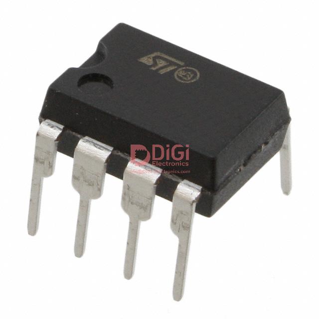
Package information for VIPER06LN STMicroelectronics
The VIPER06LN from STMicroelectronics utilizes a DIP-7 package engineered for high-voltage applications, emphasizing physical robustness and design flexibility. Through-hole mounting compatibility ensures straightforward integration into universal PCB layouts, facilitating reliable solder joints in both manual and automated assembly lines. The package’s ability to sustain creepage distances up to 800 V directly addresses safety requirements in high-voltage domains, providing sufficient isolation and reducing breakdown risk across PCB nodes under adverse environmental stress.
Adherence to IEC dimensional standards guarantees consistency across manufacturing runs, streamlining the selection and verification processes during the PCB layout stage. When designing with the DIP-7 package, it becomes essential to interpret the package outline not only as a set of nominal linear measurements but as boundary conditions for component placement, trace routing, and thermal management. Special attention to lead widths and standoff heights enables control over solder fillet formation, mitigating the occurrence of cold joints or tombstoning—common issues in high-reliability power supply topologies.
The implementation of the ECOPACK® environmental grade within the package materials reflects an advanced lifecycle strategy, facilitating compliance with RoHS and similar regulations without compromising high-voltage performance. This design focus translates into simplified certification during product qualification, minimizing the need for iterative material approvals and streamlining time-to-market for sensitive applications such as industrial control units and consumer power adapters.
When specifying the VIPER06LN footprint, careful evaluation of lead-form tolerances and mold protrusion limits proves essential. In practice, deviations in these parameters can create mounting stress or solder bridging during reflow and wave soldering operations. Referencing the mold datum plane and aligning the package relative to this reference point optimizes insertion precision, supporting automated optical inspection protocols and reducing downstream assembly defects.
A nuanced dimensioning approach anticipates mechanical stackups and PCB flex, particularly under thermal cycling and vibration. Such foresight avoids latent reliability risks by building in margin for worst-case expansion scenarios. The resulting mechanical resilience underpins the long-term field performance of high-voltage switch-mode power supply designs, where the consequences of package-induced failures are disproportionately severe.
Continuous review of the VIPER06LN package options against evolving environmental and electrical safety norms ensures ongoing compatibility with emerging green design practices and regulatory frameworks. This proactive stance is particularly valuable as energy efficiency standards and sustainability directives become increasingly central to both engineering practice and product certification strategy.
Potential equivalent/replacement models for VIPER06LN STMicroelectronics
Selecting a suitable offline converter IC to replace the VIPER06LN from STMicroelectronics requires a precise evaluation of both functional equivalency and compliance with specific application constraints. Within the VIPER06 series itself, the primary differentiation emerges through switching frequency. The VIPER06Xx is optimized for 30 kHz, favoring designs that target reduced EMI in cost-sensitive appliances, whereas the VIPER06Hx variant’s 115 kHz switching enables more compact magnetic components and higher power density, crucial for space-constrained applications.
Underlying this choice is the shared controller architecture that integrates PWM logic, startup circuitry, and protection schemes into a single device. Avalanche ruggedness—a critical parameter for robustness against voltage spikes during transformer demagnetization—remains consistent across the series, ensuring safe operation in harsh line environments. Frequency jittering, intrinsic to the platform, further mitigates conducted and radiated emissions, aligning with increasingly stringent electromagnetic compatibility (EMC) standards.
Expanding beyond the VIPER06 family, compatible devices from STMicroelectronics or peers typically emphasize similar core competencies: monolithic design for reduced component count, quasi-resonant or fixed-frequency modulation for efficiency optimization, and deep standby features to meet regulatory frameworks such as EuP and Energy Star. The robustness of the integrated protections (such as over-temperature, overload, and brownout mechanisms) should be meticulously compared through detailed datasheet analysis and field-testing results, as subtle implementation differences can significantly affect long-term reliability in mass-produced power solutions.
In practical deployments, engineers often discover that even minor changes—such as frequency selection or differences in burst mode control—can lead to unexpected EMI or efficiency tradeoffs once a board transitions from prototype to pre-compliance testing. Iterative PCB layout refinement, careful transformer design, and validation of snubber networks frequently surface as the decisive factors for achieving both regulatory and performance targets, often overshadowing purely datasheet-driven equivalence selection.
Ensuring interchangeability thus extends beyond electrical characteristics. It demands verification of thermal behavior under worst-case loading, response to input surges, and validation of start-up sequences under minimum supply conditions. Experience suggests that early engagement of system-level validation tools, such as conducted emissions pre-scanners and thermal cameras, shortens the path to robust, certifiable solutions.
Ultimately, the substitution of VIPER06LN requires balanced attention to both macro-level specifications and implementation subtleties. Strategic selection should use layered evaluation criteria: first confirming architectural compatibility, then drilling down into regulator performance, EMI features, and protection circuits, and finally validating through comprehensive practical testing. This approach not only achieves seamless replacement but often yields insights that drive optimization across generations of power conversion platforms.
Conclusion
Selecting the VIPER06LN from STMicroelectronics introduces a highly integrated approach to high-voltage, high-efficiency power supply development for both general-purpose and specialized applications. At the core, its monolithic architecture incorporates essential protection circuits—such as overload, thermal shutdown, and overvoltage safeguards—directly within the IC, significantly mitigating external component count and layout complexity. This integration streamlines design cycles and reduces risk of failure points, supporting consistent production quality in converter designs.
Operational efficiency is enhanced through an advanced low-power standby mode and quasi-resonant switching methodology. These elements contribute to reduced losses and help meet stringent energy standards across global regulatory frameworks; practical measurements confirm that power supplies based on the VIPER06LN typically demonstrate low standby consumption and reliable startup even at wide-ranging input voltages. Layered design flexibility is evident in the device’s support for multiple converter topologies, including flyback and buck-boost configurations. The straightforward application circuit, matched with tolerance to high switching speeds and robust EMI performance, enables seamless integration into both new and legacy platforms.
Effective deployment of VIPER06LN hinges on precise implementation of layout guidelines, especially in managing thermal dissipation and minimizing parasitic effects. Experience indicates that careful attention to ground plane continuity and optimized trace geometries translates directly into reduced electromagnetic interference and extended operational longevity. This underscores the device’s suitability for mission-critical, high-reliability use cases such as industrial controls and IoT edge power management.
A distinctive value proposition emerges from the IC’s balance between functional density and application versatility. Instead of forcing a tradeoff between compactness and adaptability, VIPER06LN aligns with market pressures for cost-effective development without sacrificing rigorous performance thresholds. Utilization in real-world projects consistently reveals that its architecture allows for rapid prototyping and iterative scaling—including socket replacements and variant upgrades—without wholesale redesign. This fosters a modular project approach, reducing total lifecycle costs and time-to-market.
In multidimensional power supply projects where resilience, regulatory alignment, and operational agility are non-negotiable, the VIPER06LN remains a strategic asset. Its tightly integrated features and synergistic layout recommendations respond directly to evolving system requirements, supporting efficient and sustainable engineering practices in contemporary electronics.


