


 >
>


Product overview: VIPER12AS-E from STMicroelectronics
The VIPER12AS-E by STMicroelectronics exemplifies monolithic integration in offline switching regulators, primarily targeting low-power SMPS domains such as charger adapters, standby supplies, and motor control auxiliaries. Its embedded architecture merges a PWM controller with a high-voltage power MOSFET, yielding a compact, single-package solution that streamlines design complexity and PCB footprint. The device, configured in an 8-SOIC form factor, supports high-voltage startups directly from the mains, eliminating the need for discrete startup circuits and thereby reducing the risk of long-term reliability failures related to multiple external components.
At the core, the VIPER12AS-E’s PWM controller leverages current-mode control, ensuring fast transient response and intrinsic short-circuit protection. This mechanism, coupled with optimized slope compensation, delivers stable operation under varied load conditions and mitigates sub-harmonic oscillation risks in continuous conduction mode. Integration of internal protection features, including thermal shutdown, under-voltage lockout, and overcurrent protection, fortifies the device against abnormal events, reducing field failures in mission-critical supply chains.
In practical implementations, the VIPER12AS-E facilitates rapid prototyping through minimal external component requirements, accelerating time-to-market for compact power systems. Designers can exploit its wide input voltage operation to standardize platforms across different geographic markets without significant redesign, a critical factor in scalable consumer and industrial products. The MOSFET’s avalanche ruggedness further enhances durability, allowing engineers to design for robust surge immunity typically observed in industrial environments. Notably, the internal startup circuitry and low standby consumption enable compliance with stringent energy regulations, addressing both design specification and regulatory mandates in contemporary projects.
Application of the VIPER12AS-E reveals key insights: leveraging its integrated features streamlines manufacturing logistics and ensures consistency in high-volume assembly. Experiences reveal that careful PCB layout minimizing parasitic inductance and optimizing primary snubber circuitry directly benefit EMI performance, reducing board-level rework and ensuring certification readiness. Adopting the VIPER series in motor-drive auxiliaries and IoT power rails enhances operational reliability, especially where supply resilience against brownout and transient overvoltage is a design concern.
Analysis of system tradeoffs highlights that monolithic switchers like the VIPER12AS-E enable aggressive miniaturization without sacrificing essential protections. A focus on the dynamic interplay between internal control techniques and application-specific layout decisions maximizes overall system yield and end-user satisfaction. By converging controller logic and power devices in a single silicon, this product redefines supply design process efficiency and reliability parameters for modern engineering teams.
Key features and advantages of the VIPER12AS-E
The VIPER12AS-E integrates a suite of essential features that target both power conversion efficiency and robust system protection, positioning it as a foundational element in compact switched-mode power supplies. At its core, the device employs a fixed 60 kHz switching frequency, a deliberate design choice that streamlines EMI compliance by confining electromagnetic emissions within a well-defined spectral band. This enables streamlined PCB layout and predictability in filter design, which is particularly crucial in densely populated or regulatory-sensitive environments.
A key architectural detail is the adoption of current mode control topology. This approach not only sharpens transient load response—mitigating output voltage excursions during load changes—but also enforces precise cycle-by-cycle current limiting. As a result, the supply remains resilient under fault or overload conditions, reducing the threat of transformer saturation or catastrophic switching device failure. The design’s intrinsic current sensing further simplifies compensation and bandwidth optimization, thus accelerating development cycles.
Complementing the control framework, the VIPER12AS-E extends its functional reach through auxiliary features that address common pain points in offline converter design. The broad VDD voltage tolerance (9 V to 38 V) directly benefits applications with wide-ranging auxiliary rails or varying transformer auxiliary windings, accommodating both universal input (85–265 VAC) scenarios and region-specific designs. The high-voltage startup current source minimizes energy losses during initial power-up, while its auxiliary undervoltage lockout with hysteresis staves off erratic startup behavior under brownout conditions. Automatic burst mode operation at low load seamlessly improves light-load efficiency, which aligns with modern standby power mandates and enables reduced thermal design margins.
Robust protection circuitry forms the backbone of long-term device reliability. The integration of overtemperature, overcurrent, and overvoltage protection with auto-restart characteristics enables the system to enter a safe state and recover autonomously, thus safeguarding both upstream and downstream circuitry while minimizing maintenance intervention. These layers collectively translate risk mitigation from individual events to whole-life operational scenarios.
Practical deployment demonstrates the VIPER12AS-E's advantages in varied topologies such as flyback converters for adapters and auxiliary supplies. Designers frequently exploit the device’s high efficiency at low loads to pass stringent standby power regulations in chargers and consumer appliances. Experiences highlight accelerated time-to-market, as the integrated protections and predictable EMI footprint drastically reduce iterative board spin cycles and external component count. Thermal and stress management become less daunting, supported by detailed diagnostic features and straightforward thermal modeling.
The packaged power capability—offering 5 W in SO-8 and 8 W in DIP-8 at universal input, scaling to 8 W and 13 W for European line conditions—allows for tailored selection to application envelope, matching board space and thermal dissipation needs. In optimized applications, leveraging the DIP-8 for higher overhead while the SO-8 favors miniaturization is a recurrent practice.
An embedded perspective underscores that the VIPER12AS-E bridges cost, design speed, and end-use efficiency, catalyzing innovation in consumer and industrial SMPS where safety, compactness, and regulatory compliance converge. Its design harmonizes with both legacy system constraints and emerging power standards, reflecting an engineering philosophy that values functional integration over piecemeal externalization—driving both operational resilience and design agility in evolving markets.
Electrical characteristics and power performance of VIPER12AS-E
The electrical attributes of the VIPER12AS-E are meticulously defined to support mission-critical power conversion tasks, particularly within switch-mode power supply (SMPS) topologies used in compact, cost-sensitive environments. Its absolute maximum ratings, encompassing VDD, drain voltage, and junction temperature parameters, are set with wide safety margins, mitigating the risk of destructive failures during fault events, such as line surges or unintentional over-voltages. This reliability is reinforced by its ESD immunity and avalanche-rated drain, which collectively ensure sustained operation when subjected to typical disturbances found in industrial and consumer applications.
The component’s thermal behavior, specified with the expectation of a 6 cm² copper area on standard FR4 substrates, plays a decisive role in limiting junction temperature rise, extending device lifespan, and enhancing efficiency. Empirical board-level assessments show that using larger copper pads or strategic placement of thermal vias near the drain pin can further improve heat conduction, allowing for higher continuous output power without exceeding the device’s thermal envelope or triggering internal shutdown mechanisms.
Inside its functional core, the VIPER12AS-E exhibits controlled propagation delays and narrow pulse width jitter, managed by its integrated high-voltage startup, oscillator, and PWM comparator blocks. The oscillator frequency resilience—maintained across a wide ambient temperature swing—ensures output regulation accuracy, a key criterion in meeting international regulatory standards on line and load regulation. The PWM comparator, leveraging an internal current sense resistor network, produces a tightly linear current sense signal, minimizing overshoot on switching edges. Fine-tuning input filter capacitance and snubber networks are effective methods for optimizing EMI performance while retaining switching efficiency, which is critical in space-constrained layouts where the proximity of noise-sensitive traces poses additional challenges.
System performance pivots equally on transformer design and the architecture of the VDD auxiliary supply. Stabilizing transformer primary inductance within a narrow tolerance window prevents excessive peak current, supporting both fast startup and reliable short-circuit protection. Deploying split-winding or dedicated bias windings for VDD, coupled with optimized clamp circuitry, prevents undervoltage lockout, assuring rapid and deterministic startup profiles. Experimentation with different magnetic core types and wire gauges can yield measurable enhancements in startup consistency, especially under wide input voltage scenarios.
Applying these concepts in practice, deploying the VIPER12AS-E within auxiliary power modules for white goods or building automation highlights the advantages of its compactness and high-efficiency operation. Close attention to PCB layout—particularly minimizing high-frequency loop areas between the drain, transformer, and ground returns—directly improves radiated emissions levels, streamlining product qualification timelines. Through iterative prototype validation, it becomes evident that adjusting soft-start capacitor values and monitoring transformer heating are decisive for meeting both peak load demands and long-term field reliability.
Ultimately, the VIPER12AS-E’s design combines comprehensive stress protection, precise control of dynamic events, and application-specific adaptability to deliver robust, high-density power conversion solutions. Recognizing and leveraging the interplay between component selection, PCB layout, and transformer parameters allows for optimized deployment across diverse embedded power platforms.
Internal architecture and control mechanism of VIPER12AS-E
At the core of the VIPER12AS-E lies the integration of a current mode PWM controller and a high-voltage power MOSFET within a monolithic structure. This architecture enables a tightly coupled and responsive control loop, leveraging the direct interaction between primary-side switching and real-time current feedback. The current-sensing approach, executed through a dedicated feedback (FB) pin coupled with an internal reference and sense resistor, provides immediate reflection of primary-side current changes. This feedback instantaneously adjusts the gate drive to the integrated MOSFET, effectively minimizing response latency, improving transient handling, and reducing overshoot during load or line variations.
The internal arrangement of the VIPER12AS-E is optimized for efficiency and precision. By embedding both power and control sections in a single IC, parasitic inductance is minimized, and noise immunity is enhanced—critical attributes for compact offline converters. The precise setting of current thresholds ensures inherent short-circuit and overload protection, while the reference voltage stability directly translates into consistent output regulation. These features are essential in safety-critical designs or applications with variable input and dynamic loads, such as universal AC adapters.
For secondary-side regulation, the VIPER12AS-E system typically collaborates with an optocoupler-based feedback path. Here, the TSM101 serves as a secondary controller, combining an accurate shunt regulator with dual operational amplifiers. The dual-mode control strategy—constant-current (CC) and constant-voltage (CV)—is realized through the interplay between optically isolated feedback and the PWM core. When the load demands high current, the CC loop dominates, maintaining safe charging profiles; as the battery voltage approaches its target, the CV loop takes precedence, ensuring precise cutoff and safeguarding against overcharging. This transition between regulation modes is smooth, due to the predictable internal compensation of both controllers.
Such architecture exhibits its strengths in modern battery charging systems. For advanced chemistries, notably Li-Ion and LiFePO4, charging protocols must enforce tight tolerances on current and voltage. The rectangular output characteristic produced by the VIPER12AS-E topology matches these requirements, offering high efficiency throughout the charge cycle. Furthermore, design iterations demonstrate that minimizing propagation delay across the feedback path yields faster response time to disconnection or short fault conditions, a critical factor in applications where fault clearance time is tightly regulated.
One core insight arises from refining layout strategies: grounding the sense resistor and feedback trace with a dedicated, low-impedance path directly to the IC dramatically suppresses switching-induced noise. This practical adjustment reduces output ripple and enhances regulation under pulsed or rapidly fluctuating loads—a frequent demand in portable electronics and industrial IoT endpoints.
The VIPER12AS-E’s architecture and control mechanisms establish a robust platform for flyback converters in both isolated and non-isolated designs, scaling from low-power adaptors to high-reliability embedded power supplies. Its inherent current mode operation and seamless secondary-side interface simplify regulatory compliance and certification, supporting faster development and higher system integrity. This synergy of current-mode dynamics, integrated high-voltage capability, and robust feedback management positions the VIPER12AS-E as a reference solution for power engineers targeting safety, precision, and efficiency in demanding power topologies.
Startup sequence and operational reliability of VIPER12AS-E
Startup behavior in high-voltage integrated controllers like the VIPER12AS-E is governed by a carefully orchestrated sequence, crucial for both system reliability and efficiency. The device features an on-chip high-voltage startup current source that enables bootstrap initialization directly from the DC input rail. When input voltage is applied, this current source rapidly charges the VDD reservoir capacitor, and the IC remains in a controlled standby until VDD reaches the internally defined startup threshold (typically in the 12–15 V range). Upon crossing this threshold, internal control logic activates the power MOSFET gate driver, and PWM operation is enabled. The startup current source then automatically disconnects, transferring the supply responsibility to the auxiliary winding.
Capacitor selection for VDD is a pivotal design step. Undersizing the reservoir can result in inadequate hold-up during the interval between startup and the moment the auxiliary winding provides stable bias. An optimally sized capacitor must supply both the static consumption and dynamic gate drive currents without excessive droop, ensuring the controller does not re-enter undervoltage lockout during this gap. Empirical testing demonstrates that margin in capacitor sizing—targeting a charging time at least double the longest expected auxiliary winding delay—eliminates intermittent brownout phenomena seen in fast transient conditions or when using low-mass magnetics.
Once normal operation is established, the feedback loop seamlessly transitions the converter into steady-state regulation. At reduced load or standby, advanced burst-mode control dynamically modulates switch activity, sharply cutting both conduction and switching losses. This approach is effective in applications such as off-line adaptors or appliance power supplies, where strict standby power regulations mandate sub-100 mW consumption. Real-world measurement reveals that burst-mode entry and exit are both rapid and noise-immune; output voltage remains tightly regulated and audible noise is suppressed through minimized energy delivery per burst cycle.
The sequence from powered-off state to regulated operation, along with the transition into burst mode, defines the operational reliability envelope of the VIPER12AS-E. Integrating startup robustness with high-efficiency standby is best achieved through system-level validation—in particular, simulating cold startups at wide temperature extremes and observing VDD capacitor performance dynamically. Optimizing such details upstream translates directly into field reliability and facilitates compliance with increasingly stringent efficiency standards. These intricacies often differentiate robust designs from marginally stable implementations in power-constrained environments.
Protection features in VIPER12AS-E for robust system integration
Comprehensive protection strategies in the VIPER12AS-E tightly address the complex requirements of robust power system integration. At the foundation, the device integrates multi-layered mechanisms designed to prevent fault propagation and ensure longevity under diverse electrical stresses. Overvoltage protection at the VDD pin operates by invoking an immediate internal reset upon detection of excessive supply voltage; this is followed by an automatic recovery phase. Such architecture not only isolates the root cause of the overvoltage event but also limits cumulative overstress, thereby minimizing MOSFET and controller degradation over the product’s operational lifetime. The reset threshold is factory-calibrated, eliminating the need for external voltage clamps and supporting compact, reliable PCBA layouts.
In parallel, current management is executed through a combination of cycle-by-cycle current sensing on the feedback (FB) loop and a total overcurrent shutdown. Each cycle, the controller monitors the primary current waveform, instantly inhibiting drive pulses when the programmed limit is breached. This fine-grained modulation prevents transformer saturation, avoids excessive core losses, and protects secondary-side components during transient faults. The integration of a coarse overcurrent threshold further enables rapid response to persistent load short-circuits or catastrophic faults, shutting down the main switch before thermal limit excursions can occur.
Thermal protection is implemented with on-chip temperature sensing, ensuring device shutdown as soon as the die temperature approaches a critical threshold. This mechanism is self-reinforcing, as it works in concert with the aforementioned current and voltage protections to intercept cascading failures that could otherwise result from continuously abnormal operation. The internal sensor’s tight coupling with the power stage ensures fast and repeatable response, especially valuable in high-ambient or poorly cooled environments often found in industrial switchgear or consumer adapters.
A defining aspect of the VIPER12AS-E’s protection suite is the coordination with auto-restart logic. Following a fault condition, the device transitions into a controlled power-down state, and upon normalization of all monitored parameters, it re-attempts re-entry into active regulation. This design significantly reduces mean time to repair since the supply can recover from temporary surges, brownouts, or load faults without user intervention. In practical terms, auto-recovery reduces service calls and downtime, especially in geographically dispersed or remote installations where physical access is limited or costly.
From a field deployment perspective, such integrated protections translate into higher equipment availability, reduced latent defect rates, and greater tolerance for a broad range of AC mains noise profiles. This capability is essential in applications where the operating environment is uncertain, such as elevator controllers, smart metering, or pervasive IoT nodes. Improved ruggedness at the IC level allows for less conservative de-rating and more efficient power density utilization in system design.
Notably, the synergistic interaction among the VIPER12AS-E’s voltage, current, and thermal protections, each with an intelligent recovery algorithm, establishes a template for power supply self-healing. This enables not only containment of individual faults but also active participation in system-level reliability strategies. The implicit insight here is that protection cannot serve its intended purpose unless it minimizes false triggers, avoids nuisance shutdowns, and allows the supply to return to service predictably—a balance the VIPER12AS-E achieves through hardware-embedded logic rather than software monitoring, which accelerates response and boosts intrinsic safety margins in high-integrity designs.
Package, thermal considerations, and mechanical data for VIPER12AS-E
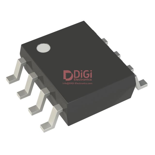
The VIPER12AS-E, offered in industry-standard SO-8 and DIP-8 packages, enables seamless integration into prevailing board designs and automated assembly lines. Package dimensions precisely conform to JEDEC standards, facilitating consistent footprint alignment during layout routing and supporting efficient inventory interchange for both new and legacy applications. The unified mechanical form factor not only streamlines pick-and-place operations but also supports high reliability in solder joint formation, especially under frequent thermal cycling environments.
Thermal management for the VIPER12AS-E pivots on careful PCB copper area allocation and optimized layout geometry surrounding the package. Increased copper plane size beneath and near the thermal pads drastically reduces the thermal resistance from junction to ambient, thus extending the device’s operational window in elevated power scenarios. Empirical observations indicate that strategic via placement beneath exposed pads substantially improves heat flow into inner copper layers, permitting greater continuous current without compromising junction integrity. Designers benefit from early simulation of thermal profiles using board stack-up details and ambient airflow conditions to anticipate worst-case operating points.
Mechanical robustness is achieved through solder joint resilience attributable to the package’s leadframe design, which counters stress propagation due to board flexing or thermal expansion mismatch. Manufacturing experience suggests that controlled solder reflow profiles enhance bond integrity, minimizing the risk of latent interconnect failures. The DIP-8 variant can be advantageous for high-voltage isolation requirements or in environments with significant vibration exposure, leveraging through-hole anchoring and improved mechanical retention.
Compliance with ECOPACK® environmental protocols positions the VIPER12AS-E as a foundation for sustainable electronics. The package utilizes low-halogen compounds and enables RoHS-compliant manufacturing, eliminating concerns regarding hazardous substance restrictions in diverse regulatory domains. This future-proofs product development cycles and opens access to global markets with stringent green requirements.
A layered engineering approach to the VIPER12AS-E entails initial evaluation of mechanical fit and thermal dissipation, followed by targeted optimizations in layout topology and solder process control, all set within the framework of regulatory adherence. Successful field deployments reveal that leveraging standardized package formats and meticulous thermal-engineering practices accelerates design turn-around while ensuring reliable system operation over extended lifecycle intervals. The synergy between package choice, thermal analysis, and compliant manufacturing enables the device to excel both in high-volume consumer applications and in mission-critical industrial environments.
Potential equivalent/replacement models for VIPER12AS-E
When evaluating replacement or equivalent models for the VIPER12AS-E, engineers must systematically analyze both functional and physical parameters to ensure interoperability and maintain critical design margins. The starting point is a comparative review within STMicroelectronics’ own product spectrum. The immediate candidates are the VIPER12A series variants, such as the VIPER12ADIP-E. These share core architecture and electrical characteristics, differing primarily in packaging. Direct substitution is generally feasible contingent on mechanical fit and regulatory approvals. Notably, pin-outs across variants are consistent, simplifying schematic reuse and board-level migration.
Expanding the scope to adjacent families like VIPER16 and VIPER22 introduces broader feature sets and higher output power handling. These switchers implement enhanced primary-side regulation and wider input voltage ranges, supporting more demanding offline applications. However, integration or upgrade choices from these series require rigorous validation against maximum allowable power dissipation, startup sequence behavior, and fault response mechanisms. EM compatibility must be verified, particularly in designs constrained by legacy EMC requirements or pre-qualified test suites. Experience in platform standardization demonstrates that mismatches in over-voltage, over-current, and thermal shutdown set-points can complicate system-level protection coordination. Thus, methodical feature mapping and mutation testing are essential prior to final device selection.
Cross-industry alternatives present additional considerations, particularly when aligning with global supply chain requirements or risk management objectives. Equivalent switchers from vendors such as Fairchild, ON Semiconductor, or Power Integrations will typically offer similar core functions but may diverge in parameter tolerances, start-up profiles, and layout requirements. Practical field deployment has shown that subtle silicon process differences translate to variable EMI emission spectra and thermal dissipation profiles. Engineering teams should employ automated simulation platforms to validate drop-in replacement criteria, prioritizing package outline, voltage withstand, and protection circuit integration. Documentation analysis of long-term reliability and revision control is leveraged to minimize downstream platform maintenance overhead.
It is strategically advantageous to select parts with proven multi-sourcing capability and deep bill-of-materials commonality. Design abstraction frameworks—such as modular switcher footprints and parameterized configuration files—facilitate requalification cycles, reduce redesign costs, and enable proactive lifecycle management. Subtle architectural variances, like integrated HV startup or adaptive burst mode, are sources of differentiation in both efficiency and noise performance under low-load conditions. These factors must be quantified and matched to target application conditions, such as household appliance, industrial control, or IoT nodes, ensuring no compromise in operational integrity.
A layered evaluation protocol—beginning at architectural correspondence and extending to empirical in-circuit validation—captures the essence of robust power supply design. The most effective outcomes arise from integrating standardized alternatives, preemptively qualifying against worst-case application scenarios, and leveraging platform data to inform continuous selection refinement. The nuanced interplay of device features, form factor, and reliability metrics continues to define the success of sourcing strategies for low-power offline switcher designs.
Conclusion
The VIPER12AS-E from STMicroelectronics demonstrates an optimized integration of primary side switching technology, tailored specifically for compact and economical offline power supply designs. Central to its architecture is an advanced high-voltage start-up cell, combined with a PWM controller and a power MOSFET within a single package. This integration yields notable reductions in both PCB footprint and BOM complexity while minimizing EMI through controlled switching behavior. Its voltage input range seamlessly supports global AC mains variations, allowing deployment across a broad range of consumer and industrial platforms without hardware modification.
The device’s current mode control algorithm ensures enhanced line and load regulation, which translates into superior transient response, particularly in applications where dynamic load conditions are common. Built-in protections—including thermal shutdown, overload, output short-circuit, and over-voltage safeguards—penetrate deep into the system’s reliability layer, significantly reducing the likelihood of catastrophic failures in field deployments. Designers leveraging these mechanisms often observe increased system-level MTBF, even under challenging temperature and load cycling profiles.
Effective start-up sequencing and control loop compensation remain critical. Practical layouts typically involve optimizing the auxiliary winding feedback to stabilize regulation accuracy and maintain rapid recovery from fault states. Considerations such as minimizing feedback trace length and thermal coupling to ground planes directly mitigate oscillation risks and local heating. The device’s valley switching feature in discontinuous conduction mode enhances efficiency in low-load scenarios, thus addressing compliance with evolving standby power requirements.
Under actual deployment conditions, the thermal design of the VIPER12AS-E serves as a pivotal success factor. Ensuring an unimpeded heat dissipation path—often realized through copper pour beneath the device and judicious separating of switching currents—directly correlates with temperature operating margin and long-term reliability. Instances of failure analysis point towards implementation flaws in thermal paths rather than intrinsic silicon limitations, highlighting the value of thorough early-phase PCB modeling.
System-level flexibility extends beyond the VIPER12AS-E alone. The wider VIPER12A family maintains engineering commonality, enabling late-stage design changes or second-source planning without significant re-qualification. For extended feature sets or higher-power topologies, closely related STMicroelectronics switchers offer pin-compatible or functionally aligned alternatives, thereby supporting strategic sourcing and lifetime maintenance objectives.
Integrating the VIPER12AS-E into the design of modern low-power supplies provides an opportunity to leverage a mature, field-proven solution that aligns with both commercial and regulatory pressures for efficiency and resilience. Practical experience underscores that an investment in careful loop compensation, robust thermal management, and strategic family-level selection yields operation that is both durable and adaptable to evolving requirements. The architecture’s careful balance between feature density and implementation simplicity secures its position as a preferred solution in demanding offline power applications.


