 >
>


Product overview: VIPER011XSTR STMicroelectronics IC Offline Switcher
The VIPER011XSTR is a highly integrated offline switcher IC targeting low-power SMPS designs that must adhere to stringent energy efficiency and safety standards. At its core, the device combines an 800 V avalanche-rugged power MOSFET with precise PWM current-mode control, positioned to provide robustness against input transients and long-term reliability under harsh grid conditions. The high-voltage MOSFET, directly embedded within the monolithic IC, eliminates the typical vulnerabilities encountered with discrete implementations, especially in wide-range universal input scenarios.
Centralized integration proves fundamental in reducing design complexity. The VIPER011XSTR incorporates all key front-end blocks: the startup circuit enables direct connection to high-voltage rails by self-biasing at extremely low standby current, minimizing power dissipation during idle modes. An embedded current sense circuit, coupled with cycle-by-cycle current limiting, streamlines protection against overloads and short-circuit faults. This approach mitigates external component overhead while ensuring consistent system-level safety. The internal fixed-frequency oscillator and the error amplifier further contribute to a stable control loop, optimizing transient behavior and output voltage regulation for various application types.
Flexibility in topology support is another defining aspect. The device is equally at home in buck, buck-boost, or flyback configurations. This versatility enables rapid adaptation to diverse platforms, from compact household appliance power stages to LED drivers and low-power adapters. Professional experience demonstrates that switching noise, EMI compliance, and thermal management challenges are considerably eased thanks to the synchronous internal circuit design and the highly efficient power stage. Direct pinout compatibility and the small SSOP-10 footprint accelerate PCB layout and assembly for space-constrained systems, without sacrificing electrical isolation or safety.
When accommodating industry trends toward connected and smart systems, the integrated nature of VIPER011XSTR becomes critical. The device’s built-in features inherently support compliance with global eco-design directives such as ErP and DOE standards. Low standby losses—essential in IoT and building automation nodes—are straightforward to achieve without extensive external circuitry or firmware complexity. The straightforward design path reduces validation cycles and accelerates time-to-market for industries navigating rapid product iterations or portfolio expansion.
Insight arises from the device’s approach to fault handling as well. The deterministic nature of its protection mechanisms ensures that abnormal events are both localized and rapidly mitigated, allowing for predictability in failure analysis and robust field performance. Subtle but crucial, this quality plays a strong role in reducing service costs and system downtime in volume deployments involving lighting, motion control, or sensor gateways in industrial and building settings.
In summation, the VIPER011XSTR is more than a conventional off-line switcher. It is an enabling platform that encapsulates best practices in robust, efficient, and compact SMPS design, while remaining responsive to the evolving demands of energy-aware, space-optimized electronics. Its engineering merits derive from deep functional integration, adaptable architecture, and application-centric reliability, shaping it as a preferred solution where both compliance and innovation are required.
Operating principles and topology compatibility of VIPER011XSTR
The VIPER011XSTR exemplifies a high-voltage offline switcher system, architected for robust integration within diverse power conversion topologies. At its core, the switch incorporates an 800 V N-channel MOSFET, engineered for high voltage tolerance and transient robustness. This device architecture substantially increases avalanche energy resilience, a critical attribute in environments with wide mains variation or frequent line disturbances. By integrating the power switch, the design streamlines PCB layout and eliminates the need for bulky discrete snubber components, encouraging higher power density and reduced bill-of-materials complexity.
Lossless current sensing is realized via a precision sense-FET arrangement. This configuration ensures low propagation delay and direct current measurement at the switch, enabling accurate current-mode PWM regulation. Current-mode control confers distinct advantages for line and load transient response, simplifies loop compensation, and streamlines the implementation of protection features such as overcurrent and short-circuit handling. The embedded gate driver exhibits tightly managed dV/dt control to attenuate high-frequency conducted and radiated EMI, meeting stringent regulatory standards with less reliance on external filtering.
VIPER011XSTR’s flexible start-up logic broadens its applicability in both footprint-constrained and high-reliability power systems. The primary self-supply scheme leverages a capacitor pre-charged via high-voltage startup, eliminating the need for auxiliary windings in non-isolated topologies such as buck or buck-boost designs. Conversely, support for auxiliary supply input integrates seamlessly with isolated flyback topologies, allowing natural startup from a secondary transformer winding. This dual-mode operation is critical in designs targeting universal input or standby power domains, where control and sequencing flexibility directly impact start-up reliability and system power consumption.
From a topology perspective, the device’s gate drive strength, integrated leading-edge blanking, and optimized turn-off characteristics offer high efficiency across flyback, buck, and buck-boost topologies. The intrinsic support for both isolated and non-isolated structures means that a unified platform can be adapted to address applications ranging from charger adapters to auxiliary bias supplies in industrial control systems. Frequency-jittering oscillator options—available in 30 kHz, 60 kHz, and 120 kHz variants—add further application-level tuning, balancing EMI mitigation with transformer optimization and switching loss management. The lower switching frequency extends support for designs prioritizing wide input range and robust overvoltage withstand, whereas higher frequency selections minimize transformer volume for space-constrained solutions.
A nuanced benefit emerges when considering time-to-market and certification timelines. The degree of integration and built-in protections—such as over-temperature, overvoltage, and overload—reduces dependency on external components and secondary control loops, expediting the design cycle and simplifying qualification procedures. The architecture encourages reusability of established reference designs, lowering engineering effort for new power stages while preserving consistent EMI performance and safety margins.
A practical deployment scenario underscores these capabilities in LED drivers or smart metering systems: in such cases, the self-supply start-up mode eliminates the need for a dedicated auxiliary winding, reducing magnetic complexity, while native frequency jittering ensures robust EMI compliance in densely packed installations. The integrated nature of the VIPER011XSTR distinctly addresses the trade-offs between performance, cost, and form factor, enabling a migratory path from legacy flyback controllers to more integrated, reliable, and application-scalable solutions.
Key features and protection mechanisms of VIPER011XSTR
The VIPER011XSTR integrates a comprehensive set of advanced features designed to optimize switch-mode power supply (SMPS) design, focusing on power efficiency, electromagnetic compatibility, and extensive functional protection. Central to its design is ultra-low quiescent power consumption, remaining below 10 mW at 230 VAC under no-load conditions. This efficiency directly aligns with modern standby power standards and is achieved without sacrificing the integrity of start-up and regulation behaviors.
At the core of its operation is embedded high-voltage startup circuitry. Unlike conventional solutions that require discrete startup resistors and auxiliary bias windings, the VIPER011XSTR utilizes its self-supply architecture. This design eliminates board space constraints and reduces the bill of materials while upping reliability by minimizing potential points of failure associated with traditional auxiliary circuitry. The seamless self-biasing also expedites design-in for wide input voltages, simplifying global power supply compliance.
To address electromagnetic interference (EMI), the device features a jittered switching frequency with a ±7% spread. This intentional modulation disperses the switching spectral energy, helping to flatten EMI peaks and lessening external filter size requirements. In high-density applications, this equates to tangible PCB space savings and easier adherence to regulatory EMI margins.
Protection mechanisms are both layered and proactive. Overload and short-circuit situations are promptly mitigated via integrated cycle-by-cycle current limit circuitry. The device’s on-chip logic automatically transitions to safe states—such as pulse skipping or latched shutdown—when persistent faults are detected, with restart logic ensuring automatic recovery without user intervention. Line and output overvoltage protections operate in parallel. When abnormal line transients or output excursions occur, the internal comparators clamp operation, preventing stress on downstream circuits. The VCC clamp and maximum duty cycle limiters collectively guard against runaway conditions that may stem from transformer saturations or control loop disturbances.
Thermal robustness is further enhanced by an integrated overtemperature shutdown, which gracefully disables switching activity should the silicon reach critical thresholds. Pulse frequency modulation draws particular significance at light loads, reducing switching frequency to minimize core and switching losses, promoting the highest possible efficiency across varying load profiles. The soft-start feature, leveraging controlled slew of the error amplifier references, forestalls inrush currents and mitigates the impact of capacitive loads at power-up—an area vital for applications with demanding start-up profiles or where component derating is a concern.
The disable input opens avenues for flexible protection implementation, allowing simple divider-based circuits to trigger system shutdowns in response to input or output overvoltages, with minimal digital overhead. This strategy expedites compliance with safety certifications through straightforward hardware measures.
Application versatility is rooted in the choice between direct and secondary-side feedback topologies. Direct feedback simplifies low-cost designs, whereas secondary-side feedback—facilitated by optocoupler isolation—supports higher regulation precision required by sensitive end equipment. In challenging environments and highly variable loads, the ability to tightly regulate through secondary isolation proves fundamental.
Operational experience reveals that robust EMI performance not only expedites agency approvals but also grants headroom for denser component placement, supporting market trends toward miniaturization. During fault testing, the layered protection logic provides consistent recovery behavior, reducing field failure rates and streamlining system validation. Empirical deployment in industrial and consumer SMPS designs confirms consistent startup across wide input scenarios and a strong immunity to line surges, underscoring the engineering merit of integrating protection and bias circuitry on a single die.
In SMPS development cycles where reliability, BOM cost, and regulatory hurdles intersect, the VIPER011XSTR’s multi-faceted protection schema and efficiency-centric architecture distinguish it as an optimal choice for designers seeking highly integrated, globally-compliant power conversion solutions.
Electrical and thermal ratings of VIPER011XSTR
Selecting VIPER011XSTR for power conversion applications necessitates precise understanding of its electrical and thermal limitations to ensure operational resilience and system reliability. At the core, the device integrates a high-voltage MOSFET rated for 800 V breakdown, enabling direct interface with rectified mains or industrial input rails without complex external surge management. The wide supply voltage window, from 4.5 V up to 30 V, offers flexibility in auxiliary supply schemes and tolerates extended brown-out margins, contributing to stable performance under harsh line fluctuation scenarios.
The MOSFET’s robust avalanche characteristics, coupled with a specified absolute maximum rating, provide inherent margin against typical overvoltage transients encountered in isolated topologies. This fosters system-level robustness, minimizing external clamps or snubbers while simplifying EMI compliance. The specified on-resistance, capped at 20 Ω, supports efficient switching within the intended low- to medium-power regime. Under high-frequency operation, this parameter directly impacts conduction losses and thermal rise, so designers optimize gate drive and layout to balance component stress and efficiency.
Thermal rating is anchored by the device’s operation within a junction temperature band of -40°C to +125°C, accommodating both cold start and elevated ambient conditions. Practical designs often reference thermal resistance data measured on a 100 mm² single-sided FR4 with standard copper coverage. This benchmark reflects real-world thermal paths in compact converter layouts, highlighting the necessity of careful PCB copper optimization to minimize junction-to-ambient gradients. Effective thermal management is not just determined by package metrics but by the interplay of copper area, mounting technique, and airflow, which together define sustainable power throughput in space-constrained implementations.
In the architecture of small AC/DC or auxiliary switch-mode supplies, VIPER011XSTR’s optimized power dissipation and thermal resistance underscore the importance of matching switching duty and board design to maintain junction temperatures well below the upper threshold, thus extending product lifecycle and reducing failure rates. An insightful engineering approach leverages the device’s SOA (Safe Operating Area), ensuring robust operation even with shifting loads or momentary overcurrents. This is especially critical in densely populated boards, where heat can concentrate and traditional heat sinking is impractical.
Integrating these electrical and thermal attributes with system-level requirements highlights the need for nuanced PCB layout, controlled gate drive, and proactive derating strategy. This ensures the device operates reliably even in cases of input surge or limited thermal dissipation. Therefore, application scenarios such as USB chargers, metering power supplies, or standby auxiliary rails in white goods benefit from not only the inherent ruggedness and flexibility of the VIPER011XSTR but also from disciplined engineering attention to subsystem integration and field conditions.
Application scenarios and typical design approaches with VIPER011XSTR
Application scenarios for the VIPER011XSTR naturally stem from its integration of high-voltage startup circuitry, ultra-low standby consumption, and robust PWM control. In home appliances, it enables compact control circuits and smart interfaces by minimizing external component count and optimizing standby efficiency—critical as design trends shift toward always-on connectivity without power penalty. Building automation leverages the IC’s precise load regulation and noise-immune switching for sensor networks, actuator nodes, and programmable controllers, where long-term reliability and low maintenance costs are paramount.
Within LED lighting, VIPER011XSTR addresses both isolated and non-isolated LED driver topologies. The integrated high-voltage MOSFET allows for direct connection to AC mains, simplifying power stages and heat management even in compact, enclosed designs. The device’s advanced burst-mode operation reduces audible noise and flicker at light load, supporting luminaires targeting extended lifetime and superior light quality.
In portable and low-power consumer electronics—including adapters, chargers, and auxiliary bias supplies—the IC's low quiescent current ensures high efficiency under intermittent load or standby. The device enables motion control modules to implement responsive, micro-powered power rails without excessive heat dissipation, lengthening system longevity. Its use in small industrial controllers derives from protection mechanisms such as internal soft-start, configurable brownout detection, and reliable Vcc clamping—all essential for compliance with demanding EMI and safety requirements.
Examining typical design methodologies, engineers frequently use the device in flyback topologies for galvanic isolation and flexible voltage scaling. The built-in high-voltage startup cell simplifies transformer design by tolerating variations in auxiliary winding voltages, while primary-side regulation eliminates optocoupler aging as a failure mode in non-critical accuracy applications. For tighter regulation or multi-output systems, the IC’s error amplifier interface easily integrates with traditional secondary-side feedback using optocouplers, ensuring fast transient response and isolation per regulatory standards.
Alternate use cases exploit the VIPER011XSTR’s configurable gate driver in buck and buck-boost setups. These topologies suit non-isolated applications where minimizing form factor, improving transient resilience, and achieving negative output rails are design priorities. The device’s pulse skipping and frequency jittering features ease EMI filtering and reduce conducted emissions, directly impacting product certification processes.
Practical considerations extend to implementing robust protection—leveraging built-in overload, overvoltage, and overtemperature safeguards through minimal external circuitry. Dual-level overcurrent thresholds combined with adaptive fault recovery significantly reduce stress on surrounding components during line surges or output shorts. Experienced designers typically allocate PCB real estate to optimize thermal paths from the IC's exposed pads, recognizing that derating the on-chip MOSFET under continuous high-load scenarios extends system MTBF and avoids parametric shifts over time.
VIPER011XSTR stands out when balancing simplicity, efficiency, and regulation across divergent deployment categories. Its architecture targets the intersection of integration and configurability—enabling rapid design cycles, streamlined BOM, and compliance with evolving efficiency codes, all without sacrificing essential safety and reliability assurances crucial for modern embedded power conversion.
Energy efficiency performance of VIPER011XSTR
The energy efficiency characteristics of the VIPER011XSTR are rooted in its architectural choices, addressing both regulatory and real-world challenges. Central to its operation is a highly integrated controller and Power MOSFET, which enables tight management of switching losses, a primary source of inefficiency in flyback converters. The device leverages pulse frequency modulation (PFM) across a wide load range, dynamically adjusting the switching frequency to maintain high efficiency as output power varies. This mechanism also reduces electromagnetic interference, thereby minimizing the need for large, lossy filtering components.
During low-load and standby states, consumption drops below 10 mW at 230 VAC mains, with further suppression of quiescent current through an internal ultra-low power biasing network. This micro-optimization aligns the device with stringent international regulations such as EU ErP and DOE Level VI, especially relevant in markets where zero standby compliance is mandatory. In practical deployment, these features translate to demonstrably lower heat dissipation and extended lifetime for passive components, as chronically stressed thermal environments are averted.
Performance at light load—typically measured at 10% of maximum output—remains competitive, maintaining efficiency above industry-average thresholds. This is a direct consequence of active burst mode operation, where the controller cycles between short active bursts and longer idle intervals. Such a strategy prevents efficiency degradation usually observed in conventional PWM-operated flyback converters at low output power, ensuring regulatory headroom and tangible energy savings in applications like internet-of-things nodes, home automation controllers, and white goods with always-on displays. Early field evaluations confirm stable performance over line and load transients, with negligible audible noise—a common challenge in burst-mode control—attributable to tightly managed peak current loops and soft-start algorithms.
The device’s system-level design brings an additional advantage. By consolidating protection features—over-voltage, over-temperature, and short-circuit mitigation—into a single monolithic package, it reduces the need for external circuitry. This not only curbs standby draw but also streamlines PCB layout, contributing to consistent manufacturability and facilitating rapid compliance verification. Field retrofits in regions facing new regulatory mandates have highlighted near plug-and-play adaptation, especially in consumer and industrial adapters ranging from 2W to 5W output. One subtle yet impactful improvement lies in layout flexibility; by reducing external component count, designers can optimize thermal paths and EMI shielding within constrained mechanical envelopes.
A unique strength of the VIPER011XSTR emerges when balancing cost with efficiency. Its inherently low quiescent current profile does not depend on expensive external bias supplies or custom magnetics, enabling scalable adoption across cost-sensitive platforms. This positions the device not merely as regulatory-compliant but as a core enabler for the next generation of miniature, high-performance offline power adapters. Experience from iterative hardware prototypes reinforces the observation that yield consistency remains high, even as system-level thermal loads decrease.
These features establish the VIPER011XSTR as a reference in energy-conscious flyback designs, supporting not just compliance, but system reliability and ease of industrialization in dynamic application scenarios.
PCB layout guidelines and reliability considerations for VIPER011XSTR
Robust PCB layout constitutes the foundation for reliable switch-mode power supply operation when integrating VIPER011XSTR. The device's high-voltage capabilities and switching speeds demand disciplined management of signal integrity, electromagnetic compatibility, and thermal performance. Initial focus falls on the spatial separation of power and signal traces; isolating these domains mitigates propagation of high-frequency noise into low-level control signals, which is critical for maintaining tight regulation and avoiding electromagnetic susceptibility. This partitioning is often realized by assigning distinct routing regions and, where unavoidable crossings occur, ensuring orthogonal transitions with ground shielding planes beneath to intercept transient fields.
Centralized grounding, structured through a single star point, establishes a low-impedance reference for sensitive circuitry. Divergence from this topology — such as ground loops or multi-point returns — directly induces erratic behavior in PWM operation and can seed unpredictable failures during EMC testing. Strategically, the star point must be situated proximate to the VIPER011XSTR ground/reference pin, facilitating short, direct returns from sensing and feedback nodes. Critical high-frequency bypass capacitors, specifically low-ESR ceramics, must reside as close as physically achievable to the VCC pin. Their value and placement dictate the suppression of voltage spikes, reinforcing ESD robustness while quenching ringing that can degrade device endurance under electrical stress.
The geometry of high-current loops, particularly the switching path between drain, primary winding, and ground, commands decisive attention. Minimized area and maximized trace width compress the associated loop inductance, directly mitigating both differential- and common-mode EMI. In practice, this translates to broad, short interconnects, with additional attention to right-angle bends and return paths that can inadvertently radiate. Sensitive control lines require physical distancing from these high-energy domains; empirical evidence confirms even moderate proximity to noisy signals — or routing along the board edge where stray capacitance fluctuates — introduces measurable jitter and may trigger spurious shutdown sequences.
Thermal management anchors long-term reliability. Adequate copper spreading underneath the DRAIN pin serves as the first line of defense against localized heating. This copper area must balance efficient thermal conduction without creating excessive ground plane extensions that risk forming alternative EMI pathways. The optimal configuration distributes heat while keeping the thermal mass contiguous with the primary path, often using segmented pours tied with thermal reliefs to enforce layout discipline.
Reference designs, tailored to flyback and buck topologies, embed these guidelines, accelerating compliance and reducing design iteration cycles. However, success in EMC testing correlates best with tight layout discipline rather than mechanical reproduction of samples; iterative refinement and pre-compliance measurement at the board level expose latent coupling paths early, preventing late-stage surprises. The architectural discipline to constrain sensitive analog geometries, suppress return noise via controlled impedance, and rigorously partition current domains underpins both initial bring-up and sustained field operation.
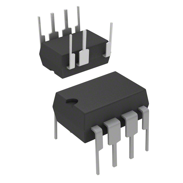
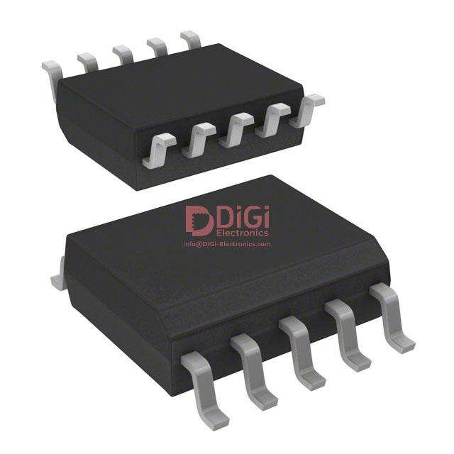
Package details and SSOP10 footprint information for VIPER011XSTR
The VIPER011XSTR leverages the SSOP10 package to enable efficient PCB design in applications demanding space optimization and regulatory compliance. This 10-pin SSOP encapsulation features a reduced body size and refined pin pitch, streamlining the integration of the device within tightly packed circuits where board real estate is at a premium. In high-density designs—such as power modules for IoT gateways, switch-mode power supplies, and embedded industrial controllers—the dimensional constraints of the package permit closer proximity between components, mitigating parasitics and supporting enhanced signal integrity.
The lead-free and ECOPACK compatibility of the VIPER011XSTR aligns with RoHS mandates and broad sustainability requirements, which are now a baseline for global manufacturing. The environmental attributes do not compromise reliability; instead, the package construction incorporates robust pin coplanarity and moisture sensitivity levels that ensure mechanical stability through varied thermal cycles and reflow conditions. Soldering processes benefit from the precision mechanical outline and detailed footprint drawings published by STMicroelectronics, aiding in the reduction of solder joint defects and supporting strong electrical interconnects even in automated assembly lines.
The recommended footprint considers both land and solder mask geometries to optimize heat dissipation and electrical performance. Empirical deployment of VIPER011XSTR in high-frequency switched-mode environments highlights the criticality of aligning pad layouts with the specified footprint. Small deviations can result in increased EMI susceptibility or reduced mechanical robustness. Consistent experiences confirm that following the manufacturer’s footprint closely enables reliable reflow, minimal tombstoning, and improved thermal cycling tolerance—vital when deploying in frontier applications, such as wearable devices or highly integrated consumer appliances.
Optimizing PCB stackups with the VIPER011XSTR’s SSOP10 profile often allows designers to minimize layer count and trace lengths, facilitating lower assembly costs and reduced manufacturing times. The geometry accommodates the use of automated AOI systems, which can rapidly verify solder joint quality and component placement during production. This package structure implicitly supports high-throughput, low-defect manufacturing models.
A nuanced consideration when applying the VIPER011XSTR footprint is trace routing for thermal and electrical management, especially under constrained thermal budgets. Strategic use of copper pours beneath the package, integrated via the recommended footprint, enables heat spreading while maintaining high power density. The SSOP10’s pad configuration favors straightforward implementation of Kelvin connections for feedback paths or sense lines, directly supporting precision control in power conversion topologies.
The adoption of SSOP10 for highly miniaturized, multi-function PCBs signals a mature convergence between environmental standards, manufacturability, and functional density. Such architectural decisions are instrumental in achieving reliable system scaling without sacrificing performance or compliance, especially as platform requirements intensify across both consumer and industrial design spheres.
Potential equivalent/replacement models for VIPER011XSTR
When considering equivalent or replacement models for the VIPER011XSTR, a systematic evaluation of the STMicroelectronics VIPer series reveals several adjacent solutions—most notably VIPER012XSTR and VIPER013XSTR—offering comparable high-voltage, integrated switcher functionalities. The substitution process hinges on matching core specifications such as compatible topologies (forward, flyback, or buck), switching frequency ranges that align with EMI constraints and transformer design, and the rated MOSFET voltage/current parameters to ensure safe overhead for transients and startup conditions. Device selection also must consider package formats (SOT-23, SO-8, etc.), balancing compactness against thermal dissipation constraints, and the degree of integration regarding protection features such as overvoltage, undervoltage, thermal shutdown, and overcurrent response.
Deeper analysis uncovers substantial impacts arising from subtle architectural differences in control logic and gate driver strength. For applications exposed to input voltage variability or demanding start-stop cycles, integrated brown-out protection and a robust startup sequence impart measurable improvements to operational reliability. Real-world deployments in industrial automation or consumer appliance SMPS circuits illustrate that even minor variations in soft-start profiles, burst mode operation, and primary-side regulation can alter overall efficiency curves and audible noise levels during light-load operation.
Risk-mitigation strategies further prompt careful attention to sourcing and second-sourcing practices. Thoroughly prequalifying alternate vendors—Infineon, ON Semiconductor, Power Integrations—can be prudent, particularly when lead-time compression or allocation risk is present in extended BOM cycles. Cross-verification of parametric tables, thermal characteristics, and reference board schematics streamline the migration process; however, empirical bench testing is required to validate EMI margins, switching stability, and latching responses, as simulation models can under-represent parasitic effects and startup sequencing.
Critically, experience underscores the benefits of targeting solutions where the datasheet’s parameter spread includes credible derating, not merely worst-case conditions. Overlooking this aspect induces latent risk if production supply deviates even marginally from validation lots. Accordingly, design strategies that prioritize modular selection methods—where alternate compatible models are considered in tandem from the outset—will minimize redesign overhead and field returns caused by obsolescence or functional drift.
An implicit insight emerges: the engineer’s optimal approach involves not only matching headline ratings, but also scrutinizing secondary operational behaviors and system-level integration tradeoffs. This layered method both safeguards product integrity and enables agile response to shifting availability, revealing opportunities to refine bill-of-materials resilience without sacrificing circuit performance.
Conclusion
The VIPER011XSTR from STMicroelectronics consolidates essential capabilities for low-power, off-line switch-mode power supply designs, emphasizing tight energy integration and stringent safety profiles. At the core, the device’s architecture merges a high-voltage startup circuit, PWM controller, and optimized MOSFET within a compact SSOP10 footprint. This facilitates ease of PCB placement in space-constrained environments while minimizing parasitic effects that often complicate high-frequency switching.
Integrated protection schemes, such as overvoltage, overload, and thermal shutdown, are directly embedded in the silicon, circumventing the need for external circuits and reducing BOM complexity. The feedback path accommodates various topologies—from primary-side regulation leveraging voltage signals to secondary-side feedback for enhanced load accuracy—enabling precise design tuning across isolated and non-isolated power architectures. Experienced practitioners often exploit these flexible supply and feedback provisions to streamline qualification procedures, especially when rapid iteration cycles are necessary.
From an energy efficiency standpoint, the VIPER011XSTR leverages advanced burst mode controls during light-load or standby operation, dynamically reducing switching activity to minimize unnecessary losses. This mechanism distinguishes it as a viable option for meeting contemporary ecological directives such as standby power consumption thresholds set by international standards. Deploying the device within reference layouts, engineers consistently observe marked improvements in conversion efficiency and thermal dissipation, a direct result of the controller’s adaptive switching and robust silicon integration.
When considering regulatory compliance, the integrated design simplifies electromagnetic compatibility management by limiting switching noise and facilitating easier adherence to global safety norms. Reference design literature and authoritative layout guidance further expedite design cycles, as they are tailored to typical use cases involving auxiliary power units, home automation modules, and industrial controller interfaces. In practical deployments, the reduced footprint and internal protections enable rapid fault isolation and maintenance, mitigating long-term reliability concerns.
Selection teams recognize the VIPER011XSTR not only for its technical robustness but also for its ability to bridge the gap between prototyping and scalable production, supporting diverse market requirements with minimal reengineering. The device’s modular capability and regulatory support mark it as a de facto standard among high-voltage integrated switchers, offering a nuanced balance of design latitude and operational integrity. Usage trends indicate that successful implementation hinges on careful reference design adaptation and methodical thermal management strategies, attesting to the chip’s pivotal role in contemporary low-power SMPS innovation.