 >
>


Product overview: VIPER26LN STMicroelectronics Offline Flyback Switch
The VIPER26LN from STMicroelectronics integrates a robust 800 V avalanche-rated MOSFET with an advanced current-mode PWM controller, streamlining offline flyback power conversion for modern low- to medium-power designs. Central to its architecture is the synergy between high-voltage switching robustness and precise pulse-width modulation, which enables tight regulation of output voltage and current. The device’s internal circuitry manages startup, steady-state operation, and fault scenarios, ensuring that transient events—such as voltage spikes or overloads—are contained without external protection components. By embedding critical functions, the VIPER26LN simplifies gate drive design and mitigates EMI concerns typically associated with discrete flyback implementations.
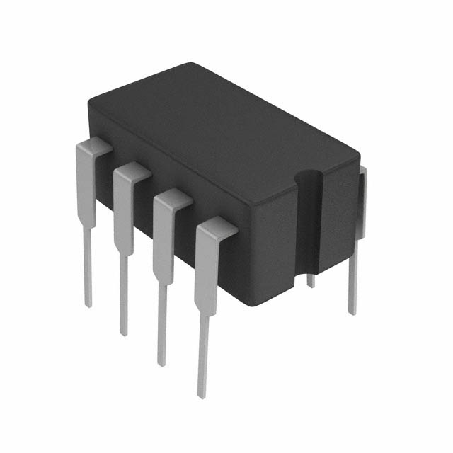
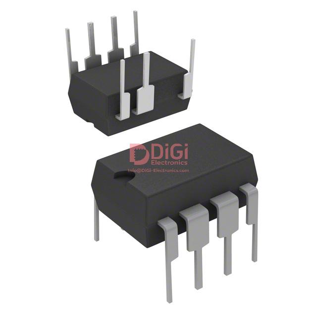
The 7-DIP compact package is engineered to optimize PCB layout for high-density designs, allowing for effective thermal dissipation while minimizing component footprint. This facilitates integration into space-sensitive applications, such as auxiliary supplies for industrial systems, smart meter power rails, and consumer electronics adapters. Its topology flexibility—supporting flyback, buck, and buck-boost converter modes—gives designers scope to customize voltage conversion stages across varied application requirements. The current-mode approach enhances dynamic response and maintains stable operation under load variation, which is critical in systems with intermittent or pulsed loads, such as LED drivers or control boards.
The device’s architecture markedly reduces standby consumption, meeting international efficiency standards for off-mode power. Optimized for minimal external component count, solutions based on VIPER26LN routinely achieve EMI compliance and streamlined bill of materials, a valuable advantage in production scale-up and regulatory certification. Integrating protections like brownout and short-circuit detection strengthens operational reliability; real-world deployment indicates rapid recovery from line anomalies and minimal downtime due to fault events. Enhanced efficiency at light and medium loads enables remote or IoT-based installations to maintain persistent connectivity without thermal or energy constraints.
Design experience reveals that leveraging VIPER26LN’s start-up circuit prevents latch-up or delayed turn-on in wide input voltage scenarios, while the integrated feedback and compensation reduce loop tuning iterations. Careful PCB layout around primary switching nodes further suppresses conducted noise, which is inherent in high-dV/dt switching environments. In practice, the device’s tolerance for network transients and its capacity to absorb energy via the avalanche-rated MOSFET translates into higher field reliability, especially in locations subject to power quality fluctuations. Successive board spins demonstrate that internal slope compensation and frequency jittering features can effectively dampen oscillations and inhibit spectral peaks, streamlining the EMI filter section and improving overall system robustness.
For applications with tight energy budgets and aggressive miniaturization constraints, the VIPER26LN presents both a practical and forward-looking solution. Its compactness and integration support a modular power strategy, paving the way for distributed architectures and rapid iteration across product families. As regulatory landscapes elevate energy efficiency and safety requirements, devices aligning high-voltage resilience with streamlined control circuits position designs to adapt with minimal revision cycles. The convergence of rigorous component integration and application-minded protection schemes in the VIPER26LN reflects a maturation in offline converter design, enabling power architectures that are efficient, agile, and inherently robust.
Electrical and thermal ratings of the VIPER26LN
Electrical and thermal parameters form the bedrock for reliable integration of the VIPER26LN in offline power conversion. The embedded 800 V MOSFET expands input voltage tolerance, directly addressing the challenge of unpredictable grid transients prevalent in widely deployed power supplies. By extending breakdown voltage thresholds, the device inherently mitigates overstress failures, which are a primary concern in industrial and consumer-grade applications interfacing with international mains. This high-voltage margin eliminates the traditional dependency on external snubber networks, streamlining the bill of materials and enabling more compact layouts without impairing EMC or long-term reliability.
Current handling capabilities are closely tied to the device's rDS(on) consistency across its -40°C to 125°C qualified junction temperature range. Low and thermally stable on-resistance minimizes conduction losses, ensuring efficiency is maintained under sustained load even during thermal excursions. This temperature resilience is particularly critical in power electronics deployed in poorly ventilated or variable ambient conditions, such as sealed adapters, smart meters, or auxiliary bias supplies in motor drives. Defining a robust operational envelope guards against thermal runaway, secures protection against latent defects, and simplifies derating calculations in automated design workflows.
Thermal conduction paths are foundational design considerations for high-density PCBs. The VIPER26LN's recommended copper area beneath the DRAIN pins functions as the primary thermal conduit, translating silicon-generated heat efficiently to the PCB plane and ultimately to ambient. In practice, performance hinges on both layout execution and stack-up: using a 1.6 mm standard FR4 substrate, even modest increases in copper spread profoundly lower junction temperatures under load. A direct correlation exists between DRAIN pad area and thermal resistance; iterative evaluation of pad geometry during prototyping often reveals diminishing returns beyond a certain footprint, emphasizing the importance of targeting optimal—not simply maximum—copper utilization.
Field deployments routinely reveal that proper adherence to mounting guidelines and careful management of thermal vias beneath the silicon footprint can extend operational lifespan by preventing localized heat stress. Deliberate integration of the VIPER26LN’s electrical tolerances and thermal strategies into the early design phase allows balancing of cost, efficiency, and reliability. Projects leveraging these best practices consistently outperform those with ad hoc thermal mitigations, underscoring an essential insight: robust thermal and electrical design integration at the device selection and PCB layout stages remains the single most effective lever for maximizing power supply longevity and reducing field failures in high-voltage switch-mode architectures.
Core features and functional blocks of VIPER26LN
The VIPER26LN integrates a set of advanced functional blocks optimized for high-efficiency, cost-conscious switch-mode power supply architectures. At the core, the device leverages a high-voltage startup circuit, enabling direct connection to rectified mains voltage while avoiding the higher static dissipation typical of external startup resistors. The result is a rapid turn-on profile with minimal energy overhead, critical for efficient standby and auxiliary power supplies operating within stringent energy regulations.
A key innovation lies in the integrated sense-FET architecture. By embedding a precision-matched current sensing element within the power MOSFET, the chip achieves cycle-by-cycle current monitoring with minimal losses and PCB parasitic effects. This approach mitigates the risk of overcurrent events and supports tightly controlled switch-off during fault conditions, addressing both safety and system reliability without adding BOM complexity or component matching burdens.
System stability and precise regulation hinge on the internal error amplifier, which, in combination with the oscillator, ensures tight feedback control even under fast load transients. The oscillator’s frequency is hardware-jittered around a 60 kHz nominal point—this randomized frequency modulation disperses EMI spectral peaks, which translates into streamlined input filter needs and easier passage through regulatory emission limits. Such an approach has demonstrated significant reductions in overall supply size and cost when compared to legacy fixed-frequency controllers, especially in space-constrained applications.
Soft-start logic embedded into the controller progressively ramps the output during initial load engagement. This mechanism not only minimizes inrush currents that could trip upstream protections but also extends component life by avoiding thermal overstress during power-up. In practical deployment, this feature has been observed to greatly improve supply startup reliability in designs where total capacitance can vary or where critical loads impose stringent sequencing demands.
Collectively, VIPER26LN’s architecture reflects a design philosophy that prioritizes integration, energy efficiency, and regulatory compliance. Beyond merely reducing external part count, each functional block is selected and configured to address real-world application pitfalls—from audible noise on EMI test benches to abnormal startup scenarios encountered in field installations. In tightly regulated markets, the inherent low standby power and robust fault management greatly simplify design qualification, translating engineering time into accelerated market reach and reduced total cost of ownership.
A unique insight emerges in the interplay between frequency jitter and sense-FET integration. The synergy allows for minimization of external components while preserving signal fidelity and regulatory headroom, offering a differentiated value proposition for designers contending with both shrinking PCB real estate and tightening energy codes. These engineering tradeoffs frame the VIPER26LN not just as a low-power controller, but as an enabler of next-generation connected and efficient power conversion platforms.
Application scenarios for VIPER26LN
The VIPER26LN’s integration of a high-voltage startup cell, primary-side regulation, and embedded protection functions anchors its versatility across diverse power conversion topologies. At the core, the device’s architecture is compatible with both flyback and buck-boost converter designs. This multi-mode operation empowers designers to optimize for space and efficiency within appliances, metering equipment, and compact LED drivers under stringent regulatory constraints.
A critical underpinning is the support for an extended input voltage range, typically up to 265 VAC and beyond. This characteristic directly addresses the challenge of global deployment in industrial or consumer electronics, where input robustness and immunity to line surges are non-negotiable. The high-voltage startup feature not only reduces external component count but also enables reliable, rapid power-up even under brownout or fluctuating grid conditions. In auxiliary power supply rails for white-goods or data acquisition modules, this translates to increased operational uptime and lower field failure rates.
Energy efficiency remains paramount amid evolving standards such as EuP and ENERGY STAR. The VIPER26LN implements quasi-resonant operation, frequency modulation, and low standby current draw. These mechanisms, working in concert, yield a compact SMPS solution with reduced core loss and minimized EMI signature—critical when deployed in environments like residential set-top boxes, IoT nodes, or metering platforms requiring <30 mW standby consumption. This efficiency is not merely regulatory; it prevents thermal buildup in sealed enclosures and supports extended product lifetimes.
From a practical viewpoint, the device's primary-side regulation eliminates the optocoupler, shrinking PCB footprint while boosting reliability. Outages due to opto-aging or feedback failures are significantly reduced, which is evident in long-lifecycle applications such as utility meters or HVAC controllers. Integrated protections—like overload, over-voltage, and thermal shutdown—enhance fault tolerance, simplifying design validation and decreasing the likelihood of catastrophic failures during voltage transients or load surges.
Leveraging the VIPER26LN also eases manufacturing logistics: a single platform can be rapidly adapted for buck, isolated flyback, or non-isolated topologies, reducing design-to-production cycles. This flexibility encourages reuse across product families with divergent voltage and power budgets, enhancing design agility and supply chain management. The ability to confidently deliver reliable, compliant, and efficient SMPS across geographies cements the VIPER26LN's reputation as a preferred engine for next-generation auxiliary rails in appliances, precision meters, advanced LED drivers, and space-constrained consumer electronics.
Pin configuration and connection guidance for VIPER26LN
The VIPER26LN, packaged in a standard 7-DIP format, demonstrates a tightly integrated approach to high-voltage converter design where each pin is optimized for operational clarity and robustness. Pin allocation follows established switching topology conventions, simplifying signal tracing and minimizing the risk of crosstalk or misconnection. The DRAIN pin, dedicated to switching node functionality, requires particular attention to its PCB footprint. Extending its copper area not only acts as a thermal conduit, dissipating switching losses effectively, but also stabilizes device performance under varying load conditions. To prevent thermal hotspots, direct thermal paths—such as wide, unbroken copper pours and the inclusion of thermal vias to underlying ground planes—should be implemented.
Functional segmentation among remaining pins streamlines system integration. The FEEDBACK and COMPENSATION pins are positioned to facilitate loop optimization, enabling close placement of loop components and reducing parasitic inductance. Tight routing lowers noise sensitivity, improving transient response and regulation accuracy. Current limit adjustment via its dedicated pin supports fine tuning over a wide range, addressing applications from compact auxiliary supplies to higher-power converter modules, while safeguarding against overload or short-circuit scenarios without external complexity.
Startup circuitry is supported through deliberate pin configuration, reducing cold-start delay and enabling low-power standby design. This aspect proves beneficial in energy-sensitive applications or where regulatory compliance with standby power is demanding, offering simplified compliance without additional supervisory ICs. The clear demarcation between high-voltage and low-voltage domains within the pinout facilitates compliance with creepage and clearance standards, especially useful in designs requiring reinforced isolation or robust EMI performance.
In practice, careful orientation of loop and power paths on the PCB layout directly impacts EMI output and efficiency. A proven technique involves minimizing the area of high-frequency current loops—most notably between the DRAIN and SOURCE pins. Routing critical analog feedback signals away from DRAIN switching activity preserves signal integrity, with additional shielding ground traces further mitigating switching transients.
The versatility of the VIPER26LN is evident in its seamless transition between isolated flyback and non-isolated buck-boost topologies. By reserving dedicated pins for feedback loop customization and startup, it accommodates precision tailoring to both eco-mode low-power and full-load high-efficiency operation, streamlining the design of universal input AC-DC converters or specialized auxiliary supplies. This flexibility, coupled with thermal and EMI optimizations inherent to the pinout, positions the VIPER26LN as a robust solution where rapid development, high reliability, and regulatory compliance are equally prioritized. Consistent positive field results affirm that thoughtful attention to layout and pin function alignment not only accelerates time-to-market but also delivers marked gains in converter durability and system-level efficiency.
Typical characteristics and circuit designs using VIPER26LN
VIPER26LN presents an integrated solution tailored for robust, efficient low-power offline AC-DC conversion. Its core performance parameters—such as supply current, reference voltage stability, MOSFET on-resistance, and breakdown voltage—directly impact both the conversion efficiency and long-term reliability of power architectures. Typical supply current versus load curves reveal minimal quiescent drain even across fluctuating conditions, supporting stringent standby power targets. Reference voltage accuracy under temperature variations safeguards downstream regulation and system timing, which is crucial for preserving both output consistency and transient response.
At the architectural level, VIPER26LN incorporates a high-voltage start-up cell, advanced PWM controller, and rugged 800 V integrated MOSFET. The tight integration minimizes external component count, streamlining PCB layout and reducing system footprint. The embedded protection circuits—overload, overvoltage, short-circuit, and thermal shutdown—work in real time, maintaining device survivability across fault profiles without external intervention. Such coordinated protection mechanisms should always be verified in early prototypes, since their interaction with board parasitics and thermal mass can slightly affect trip thresholds, especially at higher switching frequencies.
Engineers will find that the VIPER26LN’s detailed electrical characteristics enable precision design tradeoffs in buck and flyback topologies. In non-isolated buck applications, the low MOSFET R_DS(on) and smooth turn-off waveform help curtail conduction and switching losses, supporting higher efficiency at sub-10 W output levels. Flyback circuits, particularly in isolated architectures, benefit from the controller’s optimized feedback handling and transformer demagnetization timing; primary-side regulation eliminates optocoupler circuits, reducing BOM cost and enhancing reliability. These attributes simplify compliance with efficiency and EMI standards, as demonstrated by stable switching transitions and low noise profiles in test setups.
Layering practical experience onto theoretical design, the need for meticulous transformer selection in flyback topologies becomes apparent. Core saturation voltages, leakage inductance, and winding geometry all interplay with VIPER26LN’s control loops—requiring iterative bench validation to secure desired output ripple and start-up performance. Thermal coupling and heat spreading near the integrated MOSFET also merit attention; controlled airflow or strategic copper pours can flatten local temperature gradients and leverage the IC’s overtemperature protection to extend overall lifetime margins.
Application scenarios span smart appliances, metering, building automation, and compact consumer adapters. The versatility of VIPER26LN enables rapid migration between designs with minor changes to feedback and compensation networks, a key edge for scalable product families. The block diagrams and reference circuits provided by the manufacturer are starting points; adaptation to noise-critical or extended input-range contexts often involves custom snubber or EMI filter tweaks based on layout parasitics and system constraints.
Fundamentally, the VIPER26LN’s system-level integration encourages a design philosophy prioritizing simplicity, resilience, and predictable field reliability. Leveraging its robust feature set and parametric stability, engineers can minimize risk across diverse power electronics landscapes while accelerating design cycles using proven reference architectures and empirical optimization.
Power section architecture of VIPER26LN
The power section architecture of the VIPER26LN is engineered around a high-voltage n-channel power MOSFET, rated with a robust minimum breakdown voltage of 800 V. This characteristic allows operation across a broad spectrum of input voltages, withstanding line surges and voltage spikes that are frequent in industrial or consumer SMPS topologies. The device’s on-resistance, typically 7 Ω, reflects careful optimization between conduction efficiency and device ruggedness, reducing switching and conduction losses without compromising safety margins.
Integrated within the silicon, the sense-FET topology enables accurate and near-lossless current measurement. By utilizing the MOSFET structure itself for sensing, the architecture eliminates the need for external shunt resistors, thus curbing PCB space requirements and thermal dissipation hotspots. This approach not only enhances system efficiency but also simplifies current loop design, easing layout constraints associated with traditional current-sensing methods.
Thermal management is addressed by a dedicated internal sensor, providing real-time temperature feedback to the control circuitry. This mechanism supports robust protection against overheating, accommodating aggressive load profiles or compromised airflow conditions typical in compact power supplies. Practically, this internal thermal loop can reduce design time and bill of materials by negating the need for external temperature protection circuitry.
Electromagnetic interference is a critical concern during high-speed switching, particularly in high-voltage domains. The gate driver in the VIPER26LN is constructed for controlled, deterministic turn-on and turn-off characteristics. By regulating gate charge and discharge rates, the driver purposefully limits voltage and current slew rates (dV/dt and dI/dt), directly suppressing EMI generation at its root. The predictable switching profile streamlines compliance with EMC standards and minimizes parasitic oscillations often problematic in dense layouts.
A critical safety mechanism is embedded via the under-voltage lockout (UVLO) feature. Should input voltage dip beneath a specified threshold, an internal pull-down circuit swiftly discharges the MOSFET gate. This proactive action blocks any spurious conduction events during brownout conditions or system power-ups, greatly reducing risks of device damage or downstream circuit faults. This strategy eliminates the shortcomings of external RC pull-downs, offering both tighter response times and improved integration.
In practical applications, such as primary-side regulated flyback converters, the aggregate benefits of this architecture manifest in simplified power stage design, improved thermal stability, and streamlined EMI management. The interplay between integrated sensing, protection, and switching control not only reduces the need for external components but also positions the VIPER26LN as a robust solution for high-reliability environments where board space, efficiency, and safety must be balanced. The internalization of critical sensing and protection elements exemplifies a design philosophy trending towards smarter, more autonomous power devices with less external dependency and reduced system-level complexity.
High-voltage startup and internal current generator in VIPER26LN
High-voltage startup in the VIPER26LN leverages an integrated current generator directly linked to the DRAIN pin. This arrangement enables immediate device self-biasing upon AC application, eliminating dependence on external auxiliary supplies during the critical power-up phase. The internal high-voltage current source feeds the VCC capacitor, methodically ramping the supply voltage with tightly controlled current profiles. This built-in current management alleviates start-up surges, allowing for optimized component selection in space-constrained designs and improving long-term supply reliability.
The transition from initial startup to steady-state operation is orchestrated seamlessly. Once the internal supply voltage crosses the defined turn-on threshold, the controller disengages the high-voltage current generator. At this point, the onboard circuitry switches to auxiliary bias sources, often derived from a transformer winding in isolated converter topologies. This shift not only reduces dissipation by disabling the higher-loss startup generator but also enables the device to achieve ultra-low standby consumption, critical for meeting strict efficiency standards and regulatory limits in consumer and industrial power equipment.
Fault handling introduces additional complexity. In abnormal scenarios such as overloads or undervoltage lockout, auxiliary bias collapses below the minimum operational threshold. The VIPER26LN intelligently re-engages the DRAIN-based current source, re-establishing operational bias while minimizing stress on external supply rails. This mechanism offers inherent robustness by allowing repeated, controlled reattempts at startup without auxiliary support. It mitigates the risk of uncontrolled cycling and erratic restart behaviors, which are known triggers for transformer audible noise, EMI spikes, and downstream circuit stress.
Design experience points to the notable advantage of reducing external startup networks—such as high-value resistors—that traditionally present reliability challenges and consume valuable PCB real estate. The internal current generator in the VIPER26LN supports a broad input voltage range, demonstrating consistent cold-start performance even under wide mains fluctuation. In more demanding application scenarios, such as high-efficiency adapters or low-power SMPS, this approach simplifies EMI filtering and thermal profiles, accelerating certification processes and time to market.
A crucial detail often underappreciated is the coordinated control logic, which tightly synchronizes the transition between startup, normal operation, and fault recovery modes. This logic prevents any contention over bias sources, eliminating supply voltage dips and contributing to a clean turn-on sequence. Such deterministic startup and recovery behavior streamlines both validation and field deployment, setting a practical template for next-generation off-line converter designs. The architecture adopted by VIPER26LN demonstrates the engineering benefits of integrating bias management into the power device, enabling resilient, low-complexity, and future-proof power solutions.
Oscillator and jittered switching frequency of VIPER26LN
The VIPER26LN integrates a fixed switching frequency of 60 kHz with a controlled frequency jitter of ±4 kHz at a 230 Hz modulation rate. This design employs a spread-spectrum technique to reshape the spectral density of emitted electromagnetic noise. Rather than concentrating switching harmonics at fixed intervals, the modulation spreads these components over a wider frequency range. This process attenuates peak energy within any given spectral band, directly impacting EMI performance by lowering electromagnetic emission spikes commonly responsible for regulatory test failures.
Within the converter's control architecture, the frequency jitter is generated internally, synchronized to avoid overlap with system-critical timing domains and optimize the distribution of harmonics. The magnitude and rate of jitter are selected to ensure that net switching energy remains stable, preserving power conversion efficiency while altering only the temporal signature of switching transitions. Oscillator stability and the precision of jitter modulation are engineered to prevent side-effects such as output ripple modulation or interference with feedback networks. In bench-testing environments, the resulting EMI signature typically exhibits smoother profiles across measurement bands, allowing relaxation of external filter requirements without degraded power integrity.
The practical impact of this strategy is notable in low-cost, high-volume applications where EMI compliance is both mandatory and cost-sensitive. By reducing peak conducted and radiated emissions, the spread-spectrum oscillator not only makes it easier to fulfill CISPR and FCC standards but also minimizes the required footprint and complexity of input EMI filters. This outcome directly contributes to downsizing the bill-of-materials and simplifies system validation. Design teams observe that careful tuning of jitter amplitude and rate—avoiding excessive spectral dilution that could hamper efficiency or load response—is crucial for optimal results.
Advanced consideration is given to potential interaction between spread-spectrum modulation and system-level resonances. In highly integrated power boards, the modulated switching frequency softens electrical stress at critical nodes, decreasing the likelihood of unwanted ringing or cross-coupling events. This contributes to stability under transient load conditions, particularly in environments subject to variable operating profiles. The underlying mechanism exploits the non-linear response of EMI measurements to concentrated spectral peaks, balancing regulatory compliance with enhanced operational robustness.
One insight emerging from deployment scenarios is that predictable, bounded jitter—such as implemented in the VIPER26LN—offers a harmonious compromise between EMI mitigation and converter performance. Unstructured or wideband modulation can introduce noise that permeates beyond EMI concerns, affecting system reliability or even audible noise characteristics. VIPER26LN's tightly controlled approach aligns switching noise management with power integrity and component reliability, providing a repeatable and verifyable pathway to regulatory approval while maintaining strict output performance guarantees.
Soft-start and current limit adjustment in VIPER26LN
Soft-start functionality in the VIPER26LN leverages a controlled internal ramp of the drain current during power-up, ensuring suppressed inrush and preventing abrupt current surges that typically induce overstress on rectifier diodes and contribute to premature transformer core saturation. This gradual ramp-up fundamentally reduces the dI/dt seen by power-stage components, distributing the initial energy transfer more evenly and thereby extending the service life of secondary-side silicon and magnetic elements. From an EMI perspective, the absence of sharp transitions during startup also mitigates noise spikes, facilitating compliance with regulatory standards and enhancing overall system electromagnetic compatibility.
Current limit adjustability, implemented through a precise external resistor interface, permits the design engineer to calibrate the device's peak current cutoff to match specific operating conditions. This tunable current ceiling directly addresses application-to-application variations, such as output power level, load profile, and transformer size. In offline flyback topologies, for example, optimizing the current limit can sharply reduce the risk of false overcurrent tripping under momentary overloads, while providing robust protection against true secondary short-circuits. It also ensures that transformer design margins can be fully exploited—balancing core utilization and safe thermal operation—rather than being restricted by a fixed, suboptimal device threshold.
In practice, when integrating VIPER26LN into power supplies supporting variable loads, such as lighting control modules or auxiliary rails in industrial systems, the fine granularity of current-limit tuning provides a decisive advantage. An engineer matching the current threshold to both the worst-case and nominal operating conditions is able to minimize both nuisance shutdowns and excessive derating, achieving a balance between resilience and efficiency. Moreover, the consistent soft-start profile—regardless of prior fault or brownout events—avoids unpredictable inrush, ensuring coordinated interaction with downstream circuitry and facilitating hot-swap compatibility.
Proper selection of the external sense resistor calls for careful characterization. Undervaluing leads to protection gaps, while conservative oversizing unnecessarily restricts available output. Minor variances in resistor tolerance or board layout can be mitigated by iterative adjustment and validation, which the straightforward resistor-based approach of the VIPER26LN simplifies. In high-volume production, the strategy of post-assembly fine-tuning by automated optical test validates process drift without cost escalation.
A key insight underlying optimal use of these features is their synergetic role: soft-start minimizes cumulative component stress at each power-up sequence, while adjustable current limit, if precisely configured, acts as a dynamic barrier against evolving system conditions and degradation over operational lifetime. Collectively, these mechanisms embed both reliability and adaptability at the heart of the design, empowering tailored power delivery without sacrificing robust protection or manufacturing efficiency.
Feedback path management: FB and COMP pins in VIPER26LN
Feedback mechanisms in the VIPER26LN hinge on the strategic use of the FB and COMP pins, which dictate signal flow in both isolated and non-isolated converter topologies. The versatility of this approach lies in its direct handling of feedback integrity and compensation at the hardware interface. In non-isolated designs, output voltage sensing can be architected for direct feedback to the FB pin, enabling straightforward implementation of standard error correction schemes. Here, regulation is achieved via predictable RC compensation networks on COMP, allowing engineers to tune transient response and output stability with familiar design values and simulations.
In contrast, isolated topologies present more complex challenges, particularly in translating output rail deviations across galvanic boundaries. VIPER26LN achieves isolation by bypassing the internal error amplifier: feedback is optically coupled through an opto-transistor to the COMP pin, preserving noise immunity and ensuring component-level isolation where safety and regulatory standards demand it. This configuration allows the feedback loop to remain tightly controlled, yet flexible to alterations in optocoupler characteristics, parasitic elements, and desired loop bandwidth. Adaptive compensation strategies, such as the integration of dual RC networks or non-linear elements, can further optimize recovery from line disturbances and load steps.
Mode transition logic embedded in the COMP pin functionality serves as a core element in power regulation flexibility. Dynamic voltage thresholds initiate burst mode operation to improve light-load efficiency. The device actively monitors COMP potential, and, based on predefined boundaries, tailors switching frequency and pulse width modulation to suit instantaneous load conditions. Rapid threshold-crossing between modes is managed with minimal latency, contributing to tight load regulation and reduced output ripple. Engineering experience has shown that careful board layout around the COMP pin, minimization of parasitic capacitance, and precision selection of compensation elements directly influence the stability envelope, especially during mode transitions and startup sequences.
A subtle but critical insight in optimizing VIPER26LN feedback lies in understanding the interplay between error amplifier bandwidth and opto-coupler response times. Balancing RC time constants against opto-coupler saturation and non-linearity effects allows designers to maximize transient response without risking instability or overshoot. In practical application, iterative oscilloscope measurements of COMP voltage behavior during line and load transitions yield valuable tuning data, revealing regions where compensation networks require refinement. Continual adjustment of feedback and compensation, informed by both simulation and real-world response, results in robust converters that excel across diverse application scenarios, from compact adapters to complex industrial supplies demanding stringent regulation and isolation.
Burst mode operation in VIPER26LN
Burst mode operation in VIPER26LN targets stringent modern energy efficiency requirements by intelligently managing low-load conditions. When the load demand decreases, the control logic transitions into burst mode, suspending switching activity for extended periods. This reduces average switching frequencies to several hundred hertz, in sharp contrast to continuous conduction during higher loads. The benefit here is twofold: switching losses are minimized, and quiescent current consumption drops significantly, translating to lower standby power and compliance with global efficiency regulations.
The implementation relies on adaptive control circuitry that monitors feedback and promptly initiates burst intervals as the feedback voltage drops below a defined threshold. During these quiescent gaps, primary side losses are curtailed, yet fast wake-up behavior ensures output voltage regulation is maintained as soon as the demand recovers. This dynamic modulation of switching activity is especially advantageous for devices operating under varied load profiles, such as home appliances, set-top boxes, and auxiliary power supplies.
Noise mitigation in burst mode is engineered through a deliberate reduction in the drain current limit. By restricting the peak drain current during each burst pulse, the transformer magnetizing current and corresponding acoustic excitation are suppressed, pushing residual audible noise below typical hearing thresholds. This attribute not only elevates perceived product quality but also eliminates the need for additional mechanical dampening or noise-masking solutions.
Practical characterization demonstrates robust output stability even during prolonged burst intervals, provided that transformer and output capacitor values are optimized for intended load steps. For instance, selecting capacitors with stable ESR characteristics helps damp voltage deviations at burst re-entry. Deployment in high-sensitivity consumer environments has validated the VIPER26LN's ability to blend low standby consumption with a silent footprint, enabling designers to fulfill both energy and end-user satisfaction targets. Anticipating future efficiency mandates, incorporating burst mode techniques as implemented in VIPER26LN emerges as a critical enabler for next-generation power supply design, shifting the focus from raw performance to intelligent adaptability and seamless user experience.
Protection mechanisms in VIPER26LN (overload, short-circuit, open loop)
The VIPER26LN integrates a set of intertwined protection mechanisms addressing overload, short-circuit, and open-loop conditions at both circuit and system levels. For overload and short-circuit scenarios, the device employs an automatic restart logic governed by an embedded up-down counter. This timer-based logic actively monitors power delivery events, identifying both sustained overcurrent and high-stress fault signatures. When a threshold violation occurs, the up-down counter disables switching, enforcing a cool-down period before an automatic attempt to restart. This strategy not only prevents component overheating but also discourages repetitive high-stress cycling, extending overall power stage reliability. The restart interval is dynamically managed to adapt to the fault’s persistence, balancing protection aggressiveness with system uptime requirements.
For open-loop conditions, the architecture leverages feedback path diagnostics and auxiliary voltage sensing. Any feedback failure or auxiliary winding voltage anomaly is immediately flagged, prompting a rapid and controlled shutdown of the output switch. This preemptive action counters the risk of uncontrolled or excessive output voltages—common when the feedback loop is compromised—thereby safeguarding downstream circuitry and reducing exposure to catastrophic failure. Proper control of such failure modes is critical in power converter applications prone to wiring degradation, optocoupler aging, or phototransistor drift.
In field deployments, these protection paradigms have demonstrated significant practical advantages. Circuit traces seldom exhibit discoloration or localized heating, even when dummy or excessive loads are applied during test cycles. Fast response to shorted outputs or open optocoupler signals has been observed to sharply limit energy dissipation, avoiding typical collateral damage in adjacent protection circuits. The built-in correction and restart mechanisms offer maintenance-friendly operation, as devices self-recover from transient events that might otherwise prompt manual intervention.
A crucial nuance in the VIPER26LN’s design is the seamless integration of these protection features with normal converter operation, preventing nuisance trips while quickly isolating genuine faults. By balancing detection sensitivity with robust filtering, the device establishes a stable foundation for reliable offline switch-mode power supplies, even in environments prone to abrupt load variation or partial component failure. This engineering approach highlights the importance of active, context-aware protection in modern power management ICs, supporting both long-term system integrity and operational resilience.
Package options for VIPER26LN
The VIPER26LN from STMicroelectronics demonstrates a deliberate balance between thermal performance, form factor optimization, and regulatory compliance through its packaging options. Detailed attention to package architecture allows engineers to select configurations that align precisely with project constraints, whether in prototyping, mass production, or compliance-driven environments.
The DIP-7 package stands out for its universality in through-hole applications. It features robust lead dimensions that ensure reliable mechanical stability—especially in scenarios subject to vibration or mechanical stress. The generous lead pitch simplifies manual and wave soldering operations and tolerance stacking during PCB assembly. Notably, the DIP-7 package’s substantial size enables superior thermal dissipation via both component body and PCB copper area. This makes it particularly suitable for designs requiring sustained output in confined enclosures or under intermittent overload conditions, such as domestic appliance power supplies and industrial adapters. Real-world deployments of DIP-7 often benefit from lower risk of hot spots and improved power conversion reliability over extended operational cycles.
Conversely, the SO16 narrow package presents a strong argument for high-density PCB designs demanding minimized component footprint. Its narrower profile and shorter leads adapt well to automated SMD processes, streamlining mass production and reflow soldering logistics. Engineers targeting space-constrained layouts—such as IoT modules, embedded control boards, or compact chargers—can exploit SO16’s reduced footprint to achieve aggressive PCB area reductions while maintaining necessary power integrity. However, thermal management in SO16 variants typically requires deliberate routing of thermal vias and optimized copper pours adjacent to the package to maintain junction temperature margins under full-load operation.
Both packages comply with ECOPACK standards, reinforcing the synergy between advanced packaging technology and evolving environmental regulations. This addresses not only lead-free solder requirements but also facilitates certification for eco-sensitive markets, reducing potential redesign cycles associated with legislative updates.
A nuanced decision framework arises from these options. For legacy systems or repair environments where socketability and thermal mass dominate, the DIP-7 remains a pragmatic selection. In contrast, future-oriented, miniaturized platforms with tightly integrated assemblies gravitate toward SO16 narrow, provided that thermal solutions are validated early in design.
Optimal package selection for VIPER26LN is neither trivial nor generic—it is an exercise in harmonizing mechanical, thermal, electrical, and compliance attributes to the constraints and priorities of each application context. Fluid adaptation to emerging PCB technologies and environmental directives further reinforces the strategic value of diversified packaging in modern power conversion solutions.
Potential equivalent/replacement models for VIPER26LN
When addressing supply chain flexibility or accommodating design variations, examining alternative models within the VIPER26 series is essential. The VIPER26LD, for instance, mirrors the VIPER26LN in terms of switching frequency, allowing for seamless substitution within circuits where timing and dynamic response are critical. The primary distinction lies in the package configuration, which can influence thermal management, PCB footprint, and mechanical integration. Adjusting board layouts to accommodate differing package types often enhances assembly options without compromising electrical performance, as both LD and LN maintain consistent pinouts and key functional blocks.
Exploring the VIPER26HN and VIPER26HD models introduces another level of adaptability. Their elevated switching frequency facilitates improved efficiency at lower transformer sizes, potentially reducing electromagnetic interference under appropriately tuned layouts. Migrating to these versions may require minor adjustments to the associated filtering and transformer design. This means engineers must precisely validate switching losses, on-times, and thermal profiles during the prototyping stage. Integrating these variants often provides a pathway to meet tighter regulatory limits regarding standby consumption and high-density power conversion.
Direct interchangeability is enabled by the platform’s consistent core architecture—including the integrated high-voltage start-up circuitry, low standby consumption, and dual current-mode operation. Subtle variations in startup time, thermal profile, or EMI characteristics can become leverage points for optimizing cost, reliability, or safety certification. In applications with constrained form factors, prioritizing models with adaptable packages may streamline both manufacturing and qualification efforts.
In practice, careful consideration must be given to layout adaptations and passive component selection when substituting between VIPER26 series devices. Evaluating the interaction between switching frequency and external circuit elements uncovers opportunities to tune transient responses or maximize efficiency at the system level. Recognizing these underlying commonalities and distinct capabilities empowers design teams to anticipate market fluctuations, address lifecycle risks, and uphold consistent functional performance across multiple generations of hardware.
Conclusion
The VIPER26LN from STMicroelectronics integrates a high-voltage startup MOSFET and advanced PWM controller within a single, space-efficient package, delivering a robust solution for offline isolated flyback converters. At the core, the device leverages a 730 V avalanche-rugged power section, enabling direct connection to wide input AC mains and supporting applications where transient surges and voltage spikes are expected. The bespoke control architecture blends current-mode PWM with quasi-resonant and variable-frequency modulation. This adaptive multi-mode operation targets light- and heavy-load efficiency, adhering to both regulatory low-standby mandates and dynamic load-step requirements.
Precision in current-limit adjustment allows designers to optimize transformer and output stage sizing while meeting safety constraints—protection thresholds and soft shutdown features coordinate rapid fault responses without repetitive restarts, minimizing thermal stress and component aging. Active feedback control further enables tight output regulation, crucial for downstream digital loads or sensitive analog circuits. Configurable burst-mode operation is engineered to reduce primary-side switching losses during idle intervals, maximizing no-load and light-load efficiency above conventional flyback benchmarks.
Toolkit flexibility is highly evident: the VIPER26LN is offered in standard industry packages, ensuring seamless replacement or parallel adoption across product lines. This compatibility proactively addresses multi-source procurement challenges, reinforcing supply chain resilience while serving as a drop-in solution for both new designs and legacy board upgrades. During iterative prototyping, stable startup, fast transient recovery, and EMI robustness emerge as notable operational strengths, simplifying regulatory qualification and reducing time-to-market. The carefully tiered set of features supports both entry-level designs and advanced topologies seeking cost, size, and reliability improvements.
Integrating the controller and power switch not only minimizes PCB footprint but also streamlines thermal management through optimized internal layout—critical in compact consumer, industrial, and IoT power modules. Real-world deployment demonstrates the benefits of the VIPER26LN’s protections and adaptive modes, particularly in applications exposed to brownout conditions, variable loads, and stringent EMC requirements. Designers leveraging the full flexibility of feedback and protection settings achieve faster convergence between efficiency targets and functional safety certifications.
A reflection on current power supply evolution underscores the necessity for integration at the silicon—and system—level. The VIPER26LN exemplifies a synthesis of rugged hardware, intelligent control, and packaging pragmatism, offering not just technical merit but lowering the overall barrier to high-efficiency, reliable power designs in rapidly changing market landscapes.