 >
>


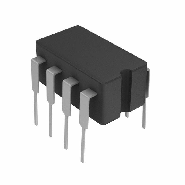
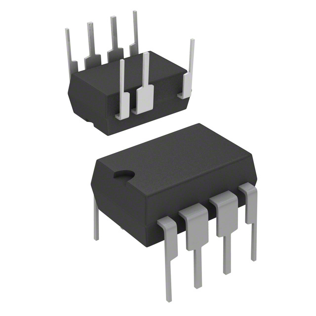
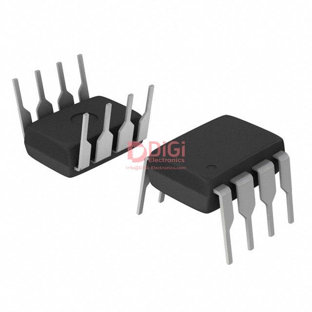
Product overview: VIPER20ADIP-E offline flyback converter from STMicroelectronics
The VIPER20ADIP-E from STMicroelectronics exemplifies advanced integration in offline flyback converter IC technology. Through a compact 8-DIP package, the device combines a PWM controller with a high-voltage vertical MOSFET rated at 700V/0.5A. This architectural integration streamlines power stage design, reducing component count and minimizing PCB footprint. The vertical MOSFET not only offers high breakdown voltage tolerance but also delivers robust switching performance, ensuring safe operation across wide input ranges. The monolithic arrangement eliminates discrete interconnections, mitigating parasitic effects and enhancing EMI behavior in power supply designs.
Underlying the device’s operational flexibility is its capability to support adjustable switching frequencies up to 200kHz. This feature enables optimal balancing between conversion efficiency and thermal management, allowing for reduced transformer sizes and improved transient response. Variable frequency selection is especially valuable during prototyping and mass production, as it aids in meeting both regulatory requirements and real-world efficiency targets. Integration of the PWM controller, with inherent protections and startup circuitry, further increases system reliability. Internal features mitigate inrush currents and offer robust over-voltage, over-current, and thermal safeguards, crucial for deployment in environments with fluctuating mains voltage or varied operational stress.
In application, the VIPER20ADIP-E demonstrates versatility across consumer, industrial, and auxiliary power contexts. For converters up to 10W with wide-range input, it maintains performance under universal AC mains, while in dedicated single-range or doubler circuits, it provides up to 20W output. The device’s intrinsic design supports rapid adaptation to different load requirements, shortening the development cycle for modular power supplies. Engineers can leverage the fast switching capability and compact layout to achieve higher density designs, crucial for space-constrained enclosures and multi-rail auxiliary systems. Practical experience shows that proper layout—especially careful ground routing and thermal dissipation—enhances noise immunity, making the device suitable for sensitive electronics.
One distinctive insight is the impact of device integration on supply chain and manufacturability. Streamlining both the BOM and assembly steps reduces points of failure and accelerates time-to-market, a priority in consumer electronics and industrial controllers. The VIPER20ADIP-E consolidates key power conversion functionalities, simplifying design validation and post-production testing. Also, its scalable approach allows reuse across multiple projects, establishing a consistent platform for future enhancements. Ultimately, the device’s engineering-focused features facilitate efficient, reliable switch-mode power supply development, promoting both functional performance and process optimization.
Key electrical and thermal performance characteristics of VIPER20ADIP-E
The VIPER20ADIP-E embodies a robust integration of power management features, distinguishing itself primarily through comprehensive electrical and thermal performance characteristics tailored for compact, high-efficiency designs. At the core, the device’s ability to sustain drain-source voltages up to 700V enables direct operation from universal AC input, simplifying the design architecture for off-line power supplies and reducing reliance on external voltage conditioning stages. The embedded power MOSFET, rated for continuous drain currents up to 0.5A and featuring an RDS(on) of 15.5Ω at 0.4A, presents an optimized trade-off between conduction losses and device ruggedness—most applicable in scenarios requiring sustained operation under moderate load while maintaining thermal stability.
Switching frequency programmability extends up to 200kHz, offering precise control over the spectral distribution of switching noise and facilitating downsizing of magnetic components. This parameter becomes vital when addressing EMI compliance and transformer volume constraints in space-limited enclosures, where leveraging higher frequency operation can lead to cost-effective miniaturization without sacrificing overall efficiency. In real-world implementations, careful frequency selection also aids in mitigating audible noise while balancing thermal dissipation across the PCB and magnetic core.
Power delivery flexibly aligns with contemporary requirements, achieving up to 10W in wide input range configurations or up to 20W with input single-range/doubler setups. The device’s power scaling ability supports designers targeting standby modes and light-load conditions typical in consumer and auxiliary supply markets. Automatic burst mode operation during standby significantly lowers quiescent consumption, ensuring sub-1W total draw—an essential parameter for compliance with global energy savings directives.
Protection features are tightly integrated: cycle-by-cycle current limiting, under-voltage lock-out, over-temperature shutdown, and soft-start act in concert, providing multilayered system resilience. These mechanisms reduce dependency on external circuitry while enhancing operational reliability. For instance, cycle-by-cycle current limiting averts thermal runaway during transient surges, and UVLO guarantees startup integrity in fluctuating mains environments, curbing the risk of erratic operation or unsafe power cycling.
Supply voltage accommodation from 8V up to 15V allows for broader compatibility with auxiliary bias networks and facilitates seamless startup sequencing in cascaded system designs. The tight definition of UVLO thresholds reinforces voltage domain protection, supporting safer transitions during supply interruptions and brownouts.
Thermal management is engineered for compact footprints, with a junction-to-ambient resistance of 70°C/W (DIP-8) and an impressively low junction-to-case resistance of 2°C/W. This balance ensures reliable junction temperatures under typical load conditions, even when heat-sinking options are restricted. In practice, optimized PCB layout—utilizing short traces and copper pours—can markedly reduce thermal gradients, sustaining long-term device endurance. The DIP package’s inherent advantage lies in its versatile mounting and cooling strategies, supporting both convection and localized heat extraction.
Ultimately, the VIPER20ADIP-E stands out by condensing advanced switching control, protection, and thermal stability into a single package, streamlining the design process while safeguarding against common application-level failures. This synthesis of features delivers consistent performance in both standalone and embedded power modules, positioning the device as a foundational building block for resilient, scalable low-power conversion architectures. Direct experience confirms that judicious tuning of programmable parameters and thoughtful PCB layout are key to unlocking the device’s full efficiency and longevity, particularly as system demands evolve toward higher compactness and regulatory compliance.
Internal architecture and operational features of VIPER20ADIP-E
The VIPER20ADIP-E integrates a suite of advanced power management functions with a precisely engineered internal architecture, enabling substantial improvements in both efficiency and operational reliability for switched-mode power supplies. At its core, the current-mode PWM controller utilizes an internally trimmed 13V reference and a transconductance error amplifier. This configuration delivers consistent voltage regulation, minimizing output ripple and maintaining stability even under rapidly changing load conditions. The transconductance error amplifier, by facilitating closed-loop control, allows for tight regulation margins and fast transient response, translating into reduced overshoot and optimized feedback behavior.
The internal oscillator is augmented with external synchronization capability, supporting applications that demand alignment across multiple power domains or strict EMI standards. This flexibility is crucial when deploying the VIPER20ADIP-E in complex assemblies, as timing requirements can be met without external clock management circuitry. The embedded logic not only orchestrates soft start sequencing—mitigating inrush currents and preventing premature stress on downstream circuits—but also provides seamless transition between shutdown and burst-mode states. Burst-mode operation, automatically invoked during light-load or standby conditions, significantly cuts switching losses. This mechanism is a primary contributor to eco-design compliance, as it maintains efficiency across variable load profiles.
Startup handling is notably robust. The integrated high-voltage current source charges the VDD capacitor, dispensing with bulky external startup resistors and reducing PCB footprint complexity. This approach simplifies layout and improves reliability by eliminating external startup failures, streamlining power-up sequences in systems requiring rapid activation.
For protection, the device incorporates real-time overcurrent sensing, utilizing a precise blanking window of 250ns to filter noise transients—an effective safeguard during electromagnetically noisy switching events. Thermal management is engineered to respond to prolonged overloads, with shutdown thresholds calibrated between 140°C and 190°C and a hysteresis margin of 40°C. This ensures recovery only after adequate cooling, preventing repetitive thermal cycling and possible substrate damage.
Practical deployment highlights the ability of the VIPER20ADIP-E to minimize board space through high integration, filter out spurious interruptions with its noise immunity window, and maintain operational continuity during adverse grid fluctuations. Its rapid startup mechanism, coupled with flexible timing alignment, caters to designs with demanding power-up and synchronization requirements. The internal architecture exemplifies a convergence of precision regulation, power saving, and comprehensive protection—a synthesis achieved without sacrificing ease of implementation or performance consistency. In scenarios where energy efficiency and fault tolerance are paramount, such as industrial or consumer power adapters, the device demonstrates marked improvements in thermal management, EMI behavior, and lifecycle stability.
Pin configuration and functional description of VIPER20ADIP-E
The VIPER20ADIP-E incorporates a compact DIP-8 pinout, engineered to balance high integration with streamlined analog control. Its pin configuration underpins both the device’s intrinsic protection features and its adaptability across topologies.
The Drain pin acts as the high-voltage entry point, interfacing directly with the input rail and serving as the current path for the integrated power MOSFET. This pin not only handles the energy transfer during switching cycles but also channels the internal startup current critical for initial device activation. Emphasis on PCB layout for this node is crucial; minimizing parasitic inductance reduces voltage overshoots, a key consideration to prevent device stress—especially during fast-switching events. Snubber networks or RC clamps are often deployed here to enhance robustness under adverse transient conditions.
Connecting all primary-side reference circuitry, the Source pin provides the system ground and returns switching currents. For compact offline designs, it is common practice to ensure a low-impedance path between this pin and the input bulk capacitor’s ground for optimal noise immunity and reduced EMI risks. In primary-side regulation modes, this node further facilitates sensing and protection circuits, as it experiences both fast switching transients and subtle ground reference shifts.
VDD powers the control section and is central to low-voltage supply monitoring. Incorporation of undervoltage lock-out (UVLO) secures the startup sequence—preventing undefined operation when supply voltage is marginal. VDD accuracy is also critical for stable operation of the internal error amplifier, which supports multiple regulation topologies. Implementing a tightly regulated, low-ESR bypass capacitor at this pin maintains supply integrity even during high dI/dt events, directly affecting PWM precision and mitigating potential latch-up scenarios.
The COMP pin embodies the feedback interface. As the output of the error amplifier, it receives the compensation network—establishing the required loop dynamics for bandwidth and phase margin specification. The pin’s high input impedance facilitates direct connection to the secondary-side optocoupler output in applications demanding isolated feedback; this approach maximizes cross-regulation performance while simplifying compensation design. Practical loop tuning often leverages adjustable RC networks here for rapid adaptation to target transient characteristics, greatly enhancing system stability in variable load environments.
Oscillator configuration is anchored by the OSC pin. Here, external components tailor the switching frequency, accommodating constraints from EMI, transformer design, and system response objectives. In designs requiring synchronization to external clocks or operation across non-standard frequency domains, this flexibility becomes instrumental—enabling phase-interleaved operation or engagement within orchestrated multi-converter systems. Consistent practice includes precise PCB layout and careful component selection at this node to prevent injection of unwanted jitter or drift.
Mastering the interaction between these pins and their related circuitry enables robust, high-efficiency designs with predictable dynamic response. Strategic layout, attention to parasitic elements, and fine-tuning loop compensation are foundational to leveraging the VIPER20ADIP-E’s strengths, particularly in wide input range and demanding offline switching applications. The pin configuration not only facilitates fundamental operation, but, if precisely exploited, unlocks enhanced protection, design agility, and resilience, positioning the VIPER20ADIP-E as a cornerstone for reliable low- to mid-power offline SMPS solutions.
Notable application scenarios and engineering considerations for VIPER20ADIP-E
The VIPER20ADIP-E stands out in power conversion applications requiring efficient, space-saving designs with high integration. Its strengths are most evident in auxiliary switched-mode power supplies for industrial systems, where operational reliability and minimal board footprint are essential. Standby power in white goods and similar household appliances also benefits from the device’s primary-side regulation, which eliminates the need for optocouplers or additional feedback paths, streamlining both hardware and validation workflows.
At the circuit architecture level, a monolithic solution like the VIPER20ADIP-E introduces crucial advantages in systems engineering. Consolidating PWM control, high-voltage startup, and MOSFET switching within a single package not only slashes component count but also reduces electrical noise susceptible points on the PCB. This integration yields a tangible decrease in field failure rates, particularly in densely populated industrial control boards, as sources of parasitic oscillation and potential hot spots are inherently minimized.
Critical design decisions revolve around transformer selection and compensation network tuning. The transformer must be wound for optimal magnetizing inductance, taking into account both minimum start-up voltage and the regulation dynamics across full load variation. Experience shows that transformers dimensioned with a margin above minimum requirements enhance start-up reliability, especially in cold or brown-out conditions. Careful evaluation of the compensation network is necessary to achieve a fast, stable transient response, especially since the VIPER20ADIP-E supports both quasi-resonant and fixed-frequency operation modes. Selecting RC values that reflect load characteristics and expected EMI constraints can make the difference between a robust SMPS and one prone to jitter or excessive conducted emissions.
Thermal management presents another layer of engineering complexity. For designs operating in the 10-20W range, internal junction temperature must be tightly controlled. Applying copper pours directly beneath the device package, along with optimizing airflow paths when possible, supports stable operation in sealed or high-ambient enclosures. In deployments where convection is limited, such as embedded power modules within appliance chassis, simulation of worst-case load and ambient conditions allows designers to preempt derating or heatsinking needs. This forward analysis avoids late-stage redesigns and field reliability issues.
On the application front, the compact form factor and simplified layout directly enable higher integration in the final product. Power supply modules leveraging the VIPER20ADIP-E often achieve PCB size reductions upwards of 20%, facilitating compliance with demanding enclosure requirements or enabling multi-output designs without penalty to losses or EMC. In particular, the chip’s robust high-voltage input tolerance and wide operating frequency range simplify global product rollouts, as designers are not forced to redesign for local mains differences or minor frequency variations. This unified approach reduces development cycles and post-deployment support needs.
Ultimately, the engineering value of the VIPER20ADIP-E is best realized when system constraints—thermal, electrical, and mechanical—are balanced holistically from the outset. A focus on transformer quality, compensation optimization, and layout diligence unlocks the full set of device benefits: minimized bill of materials, high conversion efficiency, and long-term reliability in complex industrial or consumer hardware. Integration at this level shifts design from component selection to architectural optimization, driving advances in both product performance and lifecycle economics.
Layout and implementation guidelines for VIPER20ADIP-E-based designs
Efficient VIPER20ADIP-E implementation hinges on precise PCB layout optimized for both electrical performance and long-term reliability. The foundational design imperative is the strict minimization of stray inductance along drain and source traces. Extended or meandering copper paths introduce parasitic inductance, which becomes a major source of switching noise, deteriorating both EMC behavior and transient response. Strategic placement of components, ideally maintaining the shortest possible connections between the drain, source, and critical external circuitry, mitigates voltage overshoots and supports stable, snubberless designs in lower-output power environments. Empirical evaluations reveal that the most effective configurations present less than half the typical voltage ringing seen in less-optimized layouts, correlating directly with reduced EMI emission and enhanced converter endurance.
Thermal management operates as the second design axis. The transfer of generated heat away from the device core is essential to preserve component integrity and regulatory conformity. Connecting the source pin to substantial copper pours, distributed across multiple PCB layers with carefully designed thermal vias, establishes robust thermal conduction channels. This approach leverages both the in-plane conduction of wide copper areas and the vertical conductivity through vias, ensuring temperature rise remains well below maximum junction thresholds even under full-load conditions. Observations in high-ambient environments confirm that ample source copper area can extend operating margins by up to 10°C, delaying thermal derating.
Proper isolation between high-voltage and low-voltage domains is not merely a regulatory checkbox, but a key architectural safeguard. PCB layout must enforce adequate creepage and clearance distances, especially between primary and secondary sides, to mitigate risks from both transient events and long-term tracking currents. Board partitioning and the use of distinct ground planes limit parasitic coupling, further protecting sensitive downstream circuitry. In practice, clear silkscreen barriers and physical routing of high-voltage traces along shielded board perimeters enhance both compliance and diagnostic clarity during troubleshooting.
Feedback and timing integrity depend heavily on the placement of analog loop compensation networks and oscillator-defining elements. Locating these components proximal to the COMP and OSC pins minimizes lead lengths, which in turn restricts susceptibility to high-frequency switching noise. Decoupling capacitors and RC networks benefit from direct, unobstructed paths to their reference points, enabling cleaner control signals and tighter frequency tolerance. Trials show that moving compensation networks even a few centimeters away induces measurable jitter and loop instability, underlining the necessity for compact, disciplined placement.
Across all these facets, the synthesis of fastidious layout with empirical feedback produces designs that fully exploit the integrated protections and efficiency advantages of the VIPER20ADIP-E. Adopting a holistic mindset—balancing electrical, thermal, and safety constraints from initial routing through production—consistently yields power supplies of high robustness and superior field longevity, even as designs push toward higher power densities and harsher operating conditions.
Potential equivalent/replacement models for VIPER20ADIP-E
Obsolescence of VIPER20ADIP-E necessitates careful selection of alternatives grounded in both functional equivalence and migration reliability. Initial analysis of related models within the STMicroelectronics portfolio reveals that VIPer20A-E and VIPer20ASP-E maintain core performance traits such as switch-mode operation, comparable maximum drain-source voltage ratings, and integrated protection features—including overtemperature, overload, and overvoltage safeguards. However, the distinction lies in their package formats: PowerSO-10 and PENTAWATT HV packages introduce variations in thermal dissipation and mounting flexibility, directly impacting PCB real estate and assembly strategies. These subtle differences can influence overall system robustness, especially in environments where space constraint and thermal management intersect.
Beyond direct replacements, recent VIPer series monolithic high-voltage flyback controllers offer advanced integration, improved switching frequency granularity, and enhanced EMC performance. Pin compatibility is a critical transitional concern; newer devices occasionally consolidate functions or introduce pinout modifications that require schematic adjustments. This underscores the importance of systematically mapping legacy layouts against data sheets, paying attention to start-up current, internal oscillator ranges, and the inclusion of auxiliary supply capabilities. High integration models present advantages for reducing BOM complexity and boosting manufacturing repeatability, yet close examination of protection mechanisms and latch-off behavior remains essential to avoid inadvertent reliability trade-offs.
Technical vetting should prioritize input voltage tolerance and output power capabilities in alignment with application demands. Legacy designs often operate near device limits; contemporary replacements can provide wider safe-operating-area envelopes and more sophisticated undervoltage lockout. Field experience indicates that migration success hinges on preemptive thermal modeling and gate drive assessment, particularly when transitioning to higher switching speed devices where EMI susceptibility necessitates layout optimization and component selection refinement.
Balancing backward compatibility with future-proofing, the trend favors adoption of controllers with flexible frequency programming, multi-mode operation, and high efficiency architectures that enable easier regulatory compliance. Integrated protection logic, self-biasing, and embedded current mode regulation represent structural enhancements that reduce external circuitry and streamline debugging. The evaluation process must move beyond datasheet benchmarks to reference application notes, proven design templates, and real-world failure modes observed in post-deployment phases.
Ultimately, strategic migration from VIPER20ADIP-E positions newer high-voltage monolithic flyback controllers not only as functional surrogates but as opportunities for performance uplift, system simplification, and lifecycle extension. The selection matrix should integrate engineering risk assessment, cost implications, and supplier roadmap stability, leveraging device-level advances to reinforce both legacy asset continuity and forward design agility.
Conclusion
The integration of high-voltage MOSFET power switching with intelligent PWM control in the VIPER20ADIP-E exemplifies advanced engineering in offline flyback applications. This component leverages a monolithic structure, merging power and control elements within a DIP-8 footprint, minimizing PCB space while streamlining thermal management. The adjustable switching frequency mechanism enables optimization for EMI compliance and transformer design, balancing efficiency with noise mitigation—a crucial consideration when targeting compliance with global regulatory standards.
Protection features are embedded at the silicon level, including over-temperature, overload, and over-voltage safeguards. These directly impact reliability profiles, allowing streamlined qualification workflows in both mass production and prototyping. Primary and secondary regulation capabilities unlock versatile architecture options, adapting the integrated circuit to support both feedback-driven and opto-coupler control loops. Such flexibility is essential during rapid design iterations when tailoring system-level efficiency and response time to application demands.
Ultra-low standby power consumption further distinguishes the VIPER20ADIP-E, contributing to stringent standby energy targets. Its capability of maintaining sub-50mW standby operation under high-voltage conditions addresses evolving energy standards, supporting initiatives in eco-friendly product certification. This enables deployment in IoT nodes, consumer appliances, and industrial controllers, where idle-state efficiency is prioritized.
When transitioning from this model due to end-of-life production, systematic evaluation of compatible VIPer family alternatives is imperative. Selection criteria extend beyond datasheet comparison; thermal behavior, pin compatibility, transient response, and supply chain stability should inform the migration strategy. Practical deployment experiences reveal that pre-emptive PCB layout adjustments and firmware refactoring for new control logic foster smooth replacements, reducing risk of unexpected system faults or redesign delays.
The ongoing evolution of offline flyback power solutions foregrounds integration, robustness, and configurability as central pillars. Devices such as the VIPER20ADIP-E set benchmarks for operational margins and versatility; however, future-oriented designs must anticipate obsolescence, maintain supply resilience, and leverage modular interface strategies to sustain system performance across generational shifts in power management silicon. Proven approaches—such as phased qualification of substitutes and incremental validation against real-world load profiles—drive continuity in both efficiency and reliability, reaffirming the importance of holistic lifecycle management within power electronics engineering.