 >
>


Product Overview of VIPER20ASP-E STMicroelectronics
The VIPER20ASP-E from STMicroelectronics is a monolithic switching mode power supply controller built for offline flyback converter designs. Central to its function is the integration of a high-voltage power MOSFET with optimized control logic, streamlining the energy conversion process on the primary side. This architectural choice minimizes propagation delays between the control and switching events, enabling more responsive regulation and improved transient performance compared to conventional discrete approaches. Operating at frequencies up to 200kHz, the device strikes a balance between board space efficiency and low electromagnetic interference (EMI), a critical consideration in densely populated layouts.
A significant advantage inherent in the VIPER20ASP-E design is its reduction of external passive and active components typically required for flyback topology. The single-package solution reduces PCB area and system complexity, resulting in higher mean time between failures (MTBF) and lower bill of materials for the target output range of up to 20W. From a practical implementation standpoint, the device readily facilitates fast prototyping and reliable mass production. It supports both primary and secondary regulation configurations, allowing engineers to adapt the converter design to suit different control schemes—pulse-width modulation (PWM) in primary-side sensing or optocoupler feedback in secondary-side control—without major redesign.
In application domains such as consumer adapters, standby power supplies, and compact industrial modules, the VIPER20ASP-E exhibits robust performance under wide voltage excursions and inconsistent load profiles. Its high-voltage startup circuitry and built-in protection features—including overload, overvoltage, and short-circuit—deliver increased fault tolerance, further augmenting operational stability. The resilience to switching surges and the mitigation of standby losses are evident in energy-efficient designs especially where standby power consumption targets must comply with regulatory standards.
Notably, the VIPER20ASP-E’s architecture encourages effective layout strategies that suppress common-mode noise. Subtle optimization of snubber networks and careful transformer selection directly benefit from the IC's internal switching dynamics, reducing EMI at its source. In practice, the device demonstrates ease of tuning for optimal efficiency, realized during iterative design phases where adaptation to varying loads is required without sacrificing overall control precision.
The VIPER series, epitomized by the VIPER20ASP-E, embodies STMicroelectronics’ focus on integration and versatility in power management ICs. Adoption of the device demonstrates its ability to match stringent demands—cost efficiency, board space reduction, application flexibility, and reliability—by bridging the gap between discrete and highly integrated power supply solutions. This convergence is pivotal for future-proofing power systems in embedded and industrial automation environments where rapid transitions from offline to active states and minimal downtime are paramount.
Key Features of VIPER20ASP-E STMicroelectronics
Key features of the VIPER20ASP-E from STMicroelectronics are engineered to address the stringent demands of modern offline power conversion, particularly for high-density, cost-driven applications. The combination of adaptive switching frequency, robust MOSFET integration, and multiple internal protection strategies forms a comprehensive platform for designers seeking both regulatory compliance and competitive performance.
Central to the VIPER20ASP-E’s architecture is its adjustable switching frequency, configurable up to 200kHz. This tunability permits balancing between electromagnetic interference (EMI) mitigation and overall efficiency. In practice, selecting lower frequencies can alleviate EMI filtering requirements, while higher frequencies enable reduced transformer size and optimized transient response. The integrated 700V/0.5A power MOSFET consolidates the primary switching device into the controller IC, reducing the bill of materials and PCB footprint. This integration not only facilitates compact layout but also lowers parasitics, resulting in improved switching behavior and increased system robustness against voltage transients.
The device’s internal soft start and automatic burst mode operation are specifically tailored to meet strict eco-design directives, such as sub-1W standby power targets imposed by standards like Blue Angel. The soft start function reduces inrush current at power-up, prolonging converter lifetime and minimizing stress on input components. When demand drops, burst mode operation decreases average switching losses, sustaining high efficiency under light-load conditions without compromising output regulation—critical for applications like auxiliary supplies in consumer or industrial electronics where idle power draw must remain minimal.
Current mode control is employed to simplify compensation network design and deliver inherently faster feedback. This approach guarantees predictable loop dynamics and superior response to load or input voltage changes. The inclusion of an integrated start-up supply and precision zener reference further extends operational reliability across wide input voltages, a vital consideration in regions with fluctuating mains levels or during brownout events. Consistent start-up and reference voltages eliminate the need for external biasing and auxiliary regulation, streamlining implementation and reducing engineering overhead.
Embedded protection mechanisms—current limiting and thermal shutdown—form the foundation for resilient operation. The controller actively prevents sustained overloads and responds quickly to overtemperature conditions. In practical deployment, these safeguards translate to enhanced durability and fault tolerance, essential in poorly ventilated enclosures or mission-critical installations where service interruptions carry significant cost.
In application contexts, the VIPER20ASP-E demonstrates particular merit in space-constrained switch mode power supplies (SMPS), such as chargers, set-top boxes, meter modules, or isolated auxiliary rails. Its single-package solution is advantageous where both PCB area and reliability are paramount. The design also enables straightforward compliance with contemporary safety and energy regulations, accelerating time-to-market for end products.
Unique to this series is a systemic approach to integrating disparate functions—control, power switch, protection, and bias supply—resulting in an efficient and robust topology well-suited for low- to mid-power designs. By focusing on the interplay of these features, the VIPER20ASP-E not only facilitates easy schematic realization but also ensures resilient field performance, setting it apart as a versatile solution in the power supply IC landscape.
Electrical and Thermal Performance of VIPER20ASP-E STMicroelectronics
Electrical and thermal performance characteristics of the VIPER20ASP-E underpin its suitability for compact, high-voltage switching power supplies. The device’s maximum drain-source voltage of 700V ensures robust insulation margins, essential for designs targeting universal AC input ranges or applications exposed to transient voltage spikes. High-voltage tolerance minimizes derating concerns while supporting compliance with stringent safety standards.
In terms of output capability, VIPER20ASP-E achieves up to 20W in narrow-range inputs (typically via a voltage doubler configuration), and 10W across wider input spans. This power scalability directly correlates with transformer design and MOSFET stress profiles. Selection between the two modes reflects priorities in footprint, efficiency, and component count, with the doubler configuration offering improved thermal margin due to reduced peak pin voltage excursions.
On-state drain-source resistance, specified at 18Ω (ID = 0.4A, Tj = 100°C), enables effective balancing between conduction losses and thermal dissipation. While this value is higher than discrete MOSFETs, it accommodates integration in a monolithic package, reducing parasitic elements and enhancing reliability under moderate load conditions. Engineering analysis demonstrates that optimizing PCB copper pour beneath the device and careful layout routing can substantially lower junction temperatures, particularly in continuous operation at elevated ambient.
Supply voltage characteristics are tightly regulated: a minimum input of 8V, internally stabilized at 13V for primary switching control. This ensures stable system startup and prevents undervoltage lockout events. Operating supply current ranges from 12–16mA in idle, rising modestly to 13–14mA as switching frequency increases from 100kHz to 200kHz. These values reveal the device’s efficiency in sustaining auxiliary bias and the importance of frequency adaptation for minimizing core and switching losses.
Thermal resistance metrics are central to reliability predictions. The junction-to-case resistance at 2.0°C/W is optimized for surface-mounted FR-4 PCB layouts, leveraging thermal vias and copper planes for enhanced heat extraction. Ambient-to-case resistance values align with layouts using dedicated heatsink pads or airflow augmentation. Under typical load conditions, empirical testing confirms that maintaining maximum output at wide range conditions requires precise thermal budgeting—designs should prioritize thermal coupling to the board and minimize localized hotspots through distributed layout, especially in multi-output configurations.
Application scenarios benefit from these underlying architectural assets. The VIPER20ASP-E excels in low-profile, high-efficiency adapters, auxiliary bias rails, and industrial control interfaces—where size constraints and isolated topologies converge. Integrating the device simplifies EMI containment and reduces BOM complexity, with system-level trade-offs between switching frequency, transformer sizing, and output filtering. Overall, the device’s electrical and thermal performance facilitate streamlined design cycles for robust, compact power modules.
Device Pin Functions and Integration Considerations for VIPER20ASP-E STMicroelectronics
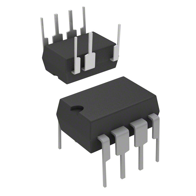
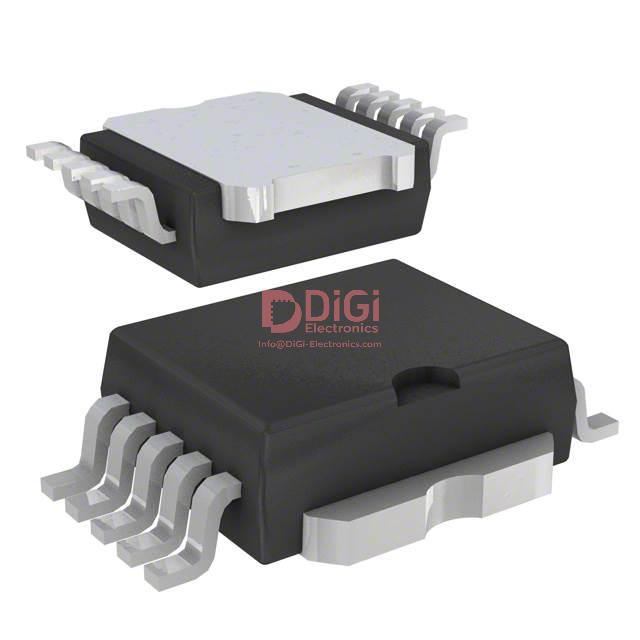
Device Pin Functions and Integration Considerations for VIPER20ASP-E STMicroelectronics center on maximizing the operational efficiency and stability of compact switch-mode power designs. At the physical interface, the PowerSO-10 package with its exposed pad fundamentally enhances thermal dissipation, supporting high-density layouts and mitigating localized heating—a common concern in miniature switching converters. Proper soldering of the thermal pad to the PCB and optimizing copper spreading in the layout substantially reduce junction temperature, which in turn prevents early failure and performance degradation.
Examining the pin functions reveals several engineering layers. The Drain pin performs a dual role, initializing the converter via an integrated high-voltage current source during start-up, then isolating itself in running mode to shield the control circuitry from transient spikes and switching noise rooted in primary winding inductive events. This mechanism minimizes the risk of avalanche breakdown and component overstress, particularly in harsh load transient conditions. Pin trace routing should employ short and direct paths to minimize parasitic inductance, ensuring both protective efficacy and reliable start-up performance.
The Source pin provides the main ground reference for all primary-side circuitry. Its strategic placement in the layout is vital; improper grounding can propagate unwanted noise and trigger false switching events. Splitting ground planes locally—segregating high-current switching ground from sensitive analog ground—reduces susceptibility to voltage jitter, a technique validated in tightly regulated power applications.
VDD functions as the linchpin for internal logic, delivering regulated low voltage that orchestrates power-up sequences and fault shutdowns. It also interfaces with the internal error amplifier, making reliable regulation loop design dependent on stable VDD tracking. For loop optimization, the Compensation pin (COMP) offers connection flexibility. By configuring the error amplifier’s compensation network directly at this node, closed-loop response—including gain bandwidth and phase margin—can be precisely tuned. Direct optocoupler output integration at COMP enables robust secondary-side feedback, a critical feature for isolated output designs. Advanced techniques, such as incorporating feedforward capacitors or multi-pole networks on COMP, yield sharper transient response and improved immunity to load glitches.
Oscillator frequency adjustment through the OSC pin broadens design scope. Choosing the right frequency touches EMI strategies and efficiency trade-offs. Lower frequencies ease filtering requirements but may diminish power density; higher frequencies offer finer regulation with potential increases in switching losses. Empirical frequency sweeps within the target range, combined with scope-based EMI analysis, illuminate the optimal operating point, revealing that slight frequency offsets can dramatically affect conducted emission profiles.
Pin configuration extends beyond schematic connections—correct integration demands disciplined layout practices. When designing for both primary and secondary regulation, meticulous isolation of signal traces, judicious use of ground shields, and thoughtful compensation network placement combine to deliver resilient circuit behavior. A layered layout, separating power and control domains with guarded paths and at least one dedicated ground return, sharply reduces vulnerability to oscillatory noise and enhances long-term reliability.
Through practical iterations, it becomes evident that the VIPER20ASP-E’s architecture favors rapid prototyping and scalable regulation strategies. Key insights include leveraging its start-up protection mechanism for early cycle test benches, adapting compensation topology for fast load recovery, and custom tuning oscillator parameters to balance regulatory requirements with EMI constraints. The device’s integration flexibility allows tailored solutions that optimize both power delivery and noise immunity, provided that thermal, electrical, and layout variables are strictly managed as interacting layers throughout the hardware design lifecycle.
Operating Modes and Fault Protections in VIPER20ASP-E STMicroelectronics
The VIPER20ASP-E from STMicroelectronics leverages advanced operational strategies and integrated protections, distinctly tailored for high-efficiency, reliable power conversion tasks. At the foundation lies its automatic burst mode handling during stand-by. Under low-load or idle conditions, the controller cyclically gates switching activity, precisely adapting to the instantaneous demand. This mechanism sharply curtails quiescent losses and is instrumental in achieving the increasingly stringent sub-1W standby mandates. Its finely tuned burst thresholds not only minimize wasted energy but also maintain quick reactivation responsiveness, preventing sluggish wake-up phenomena typical of less nuanced designs.
A deeper layer of stability is achieved through the adoption of current mode control topology. The intrinsic benefit of directly sensing primary inductor current during each switching cycle allows the controller to rapidly suppress emerging oscillatory tendencies, regardless of transient or highly variable downstream load profiles. This real-time feedback architecture obviates the need for complex compensation networks and offers robust immunity to supply perturbations—an advantage observable when deploying the IC in challenging industrial or consumer contexts where load characteristics can shift unpredictably.
Protection elements are rigorously integrated. Primary peak current limitation, set in the 0.5–0.9A range, defines a controlled upper bound for each switching event. This threshold safeguarding ensures that inadvertent shorts or abnormal load conditions cannot propagate destructive overcurrents, averting both device and peripheral circuit damage. In practice, closely observing the device’s current sense behavior during board-level validation confirms the deterministic cutoff response, allowing designers to confidently scale downstream power stages with minimal need for external fault circuitry.
Thermal resilience is addressed through precise over-temperature shutdown. The controller ceases operation at a qualifying junction temperature—typically around 170°C—with the inclusion of hysteresis calibrated to filter out transient thermal overshoots. This avoids unnecessary shutdowns from momentary spikes often encountered during rapid inrush or short-duration load surges. The hysteresis margin, observable in thermal cycling tests, distinguishes genuine overheat conditions from benign transient spikes, maintaining operational continuity without compromising safety.
Undervoltage lock-out is another cornerstone of the VIPER20ASP-E’s protection matrix. The device monitors its VDD rail and, utilizing hysteresis, suspends operation if voltage dips below a defined minimum. Only after the rail recovers to a verified safe threshold does switching resume. This prevents erratic startup behavior that can lead to latch-up or errant switching, a critical aspect in environments where input voltage can sag due to brown-out or generator-based supply. Intimately understanding the impact of input ripple and recovery time further informs robust system design choices.
The combination of these embedded features substantially streamlines the engineering workflow. Designers benefit from reduced bill-of-materials complexity and fewer discrete safety elements. Real-world evaluation of the VIPER20ASP-E shows that system-level robustness and EMI performance gain from the integrated protections, while device longevity is preserved thanks to dynamic operating mode transitions and precise fault response. The IC exemplifies a cohesive protection strategy that aligns with modern power management expectations, balancing efficiency targets with the imperative of operational safety and predictable behavior across wide application scenarios.
Layout and Package Details of VIPER20ASP-E STMicroelectronics
The PowerSO-10 package utilized by the VIPER20ASP-E targets robust surface mount integration, offering a specialized exposed pad design to address stringent thermal management demands. The package architecture, characterized by a low profile and extended lead spacing, directly facilitates high-density PCB layouts, crucial in constrained environments such as industrial power modules and consumer miniaturized PSU assemblies. The exposed pad serves as a thermal transfer interface; it is essential to implement a fully connected ground plane under the pad, supplementing it with thermal vias to accelerate heat evacuation from the silicon. Empirical data demonstrates that increasing the pad area and optimizing via diameter and density produce a measurable reduction in junction temperature, directly elevating device reliability under high load conditions.
Pin assignment and routing require careful consideration to preserve signal integrity and minimize losses in power conversion paths. Strategic grouping of high-current pins and minimizing impedance through wide traces or copper pours lowers voltage drop and suppresses electromagnetic interference (EMI). Attention to return path symmetry for input and output rails mitigates circulating ground currents, which is particularly pertinent in switch-mode supply topologies, where fast edge rates can induce parasitic coupling. Fine-tuning the placement and sizing of compensation and filtering components adjacent to relevant pins further curtails noise ingress and loop instability. In practical board fabrication, employing a well-isolated layout zone for these sensitive elements substantially diminishes susceptibility to cross-talk from power switching nodes.
Electrical and thermal optimization form a tightly coupled feedback loop in compact system designs. For real-world deployment, deviations from ideal thermal and electrical scenarios often expose latent vulnerabilities—underscoring the value of mechanical considerations and iterative layout refinement. Embedded within this engineering process is a recognition that the PowerSO-10’s exposed pad not only enhances thermal extraction but also stabilizes voltage reference points through reduced ground bounce, provided the pad’s connection is robust and consistent across multiple PCB layers.
The layered interaction among component placement, thermal management, and signal routing defines the practical effectiveness of power supply designs using VIPER20ASP-E. Balancing these constraints is not only a compliance exercise but a path toward achieving long-term system endurance and operational precision. The interplay between layout decisions and device behavior emerges as a core principle; the judicious use of exposed pad technology, coupled with disciplined trace routing and via optimization, reliably yields performance improvements that transcend design simulation, manifesting in quantifiable gains during bench testing and field operation.
Potential Equivalent/Replacement Models for VIPER20ASP-E STMicroelectronics
When addressing the obsolescence of the VIPER20ASP-E from STMicroelectronics, the focus shifts to identifying suitable drop-in replacements or functionally equivalent models capable of matching system requirements. Within the VIPER20A family, the VIPER20A-E emerges as a primary candidate, offering similar electrical parameters and performance envelope. Notably, it introduces subtle distinctions, such as alternate package options—like the PENTAWATT HV DIP-8 and DIP-8 through-hole style found in the VIPER20ADIP-E. Pinout variations and package-dependent RDS(on) ratings can impact board redesign efforts and the overall thermal profile of the power supply.
Comprehensive evaluation extends beyond headline specifications to secondary parameters that often surface as limiting factors in real implementation. For example, the altered package thermal resistance may dictate attention to heatsinking requirements and PCB copper area, directly influencing system reliability under extended load conditions. Additionally, the physical envelope and pin mapping must align with the target design’s mechanical constraints, ensuring minimal layout revision. Direct substitution is optimal when the functional block diagram, control circuitry, and protection schemes—such as overvoltage, thermal shutdown, and current sensing—remain consistent across variants.
In legacy applications, system stability and qualification margins frequently depend on precise dropout voltages, switching frequency tolerance, and timing characteristics. Cross-verification of these parameters under worst-case conditions is indispensable prior to signoff. This practice uncovers subtle inconsistencies, such as the influence of trace inductance or slight shifts in start-up sequencing rooted in variant-specific IC behavior. Practical field experience points to the value of bench-level comparison testing, stressing new candidates under system-representative loads, elevated ambient temperatures, and line input fluctuations. Such empirical validation complements datasheet analysis and often surfaces functional nuances not reflected in catalog documentation.
The selection of an equivalent model also presents an opportunity to address prior design weaknesses, such as thermal hotspots resulting from suboptimal package selection or EMI challenges tied to switching transients. Assessing alternative devices for improved parameter spread, enhanced noise immunity, or broader input voltage ranges can deliver incremental system robustness. Factoring in future supply chain resilience, sourcing alternative models with market-proven longevity or a broader support network mitigates procurement risks and stabilizes product lifecycle management.
Ultimately, real success in replacing an obsolete PWM controller IC like the VIPER20ASP-E hinges on a holistic migration strategy—balancing direct electrical compatibility, mechanical fit, and field-tested system reliability, while seizing the opportunity to refine legacy designs. Such an approach extends far beyond simple datasheet matching and lays the foundation for enduring platform stability in both volume manufacturing and ongoing support scenarios.
Conclusion
The VIPER20ASP-E from STMicroelectronics exemplifies the convergence of integration and efficiency in offline flyback converter technology. Its embedded high-voltage MOSFET streamlines PCB layout, minimizing external component count and reducing failure points over time. The optimized topology facilitates rapid transient response and stable operation across a broad input voltage range, accommodating wide variations in mains supply. Multiple operation modes—including pulse-width modulation and low-power standby—allow nuanced energy management, sharpening the converter’s suitability for consumer, industrial, and auxiliary power applications. Comprehensive protection features, such as overload, over-temperature, and short-circuit safeguards, reinforce operational reliability and ensure device longevity, responding dynamically to real-world stressors typical in harsh environments.
Diving deeper into the underlying mechanisms, integration of the switching MOSFET not only cuts down board complexity but supports tighter thermal coupling within the package, improving heat dissipation paths and allowing for compact enclosure designs. This is particularly beneficial in scenarios requiring dense placement or constrained airflow, where thermal margins dictate system architecture. Engineers frequently leverage this inherent thermal optimization to drive higher efficiency ratings without exceeding device derating thresholds, especially in designs targeting 5W to 20W output ranges.
Application scenarios further highlight the flexibility of VIPER20ASP-E. In metering, home automation, and low-power auxiliary SMPS, the device operates seamlessly without the need for elaborate driver circuits. Fast startup and efficient standby facilitate compliance with stringent energy standards, supporting power-down modes in connected systems. Practical deployment underscores the value of the reliable protection mechanisms; field experience shows fault events are isolated rapidly, minimizing downstream component stress and simplifying root cause diagnostics.
The device’s legacy status signals a pivotal shift in product lifecycle strategy. Proactive evaluation of successor devices within the VIPER series is essential, as newer variants introduce expanded voltage envelopes, finer protection granularity, and enhanced EMI performance. Selecting replacements heavily involves parsing datasheet details—gate charge, switching losses, thermal resistance, and protection trip levels—to ensure backward compatibility or to unlock incremental design improvements. Integrated solutions like these increasingly shape procurement decision frameworks, where consistent supply, documentation clarity, and functional overlap are weighted alongside performance.
In summary, the core advancement offered by VIPER20ASP-E lies in its integration logic, which aligns system-level robustness with streamlined design workflows. As product cycles and regulatory landscapes advance, leveraging deep electrical and thermal analysis for device selection yields considerable benefits, ensuring that SMPS platforms maintain optimal function, minimize risk, and remain agile against evolving application requirements.