 >
>


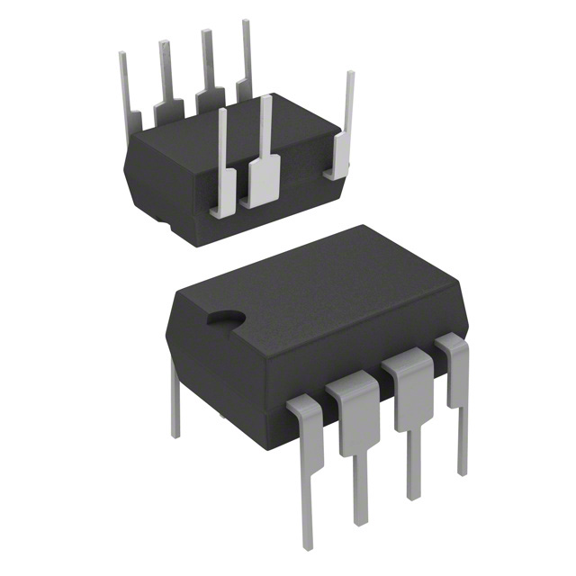
Product Overview: VIPER12ADIP STMicroelectronics IC Offline Switch 8DIP
VIPER12ADIP from STMicroelectronics exemplifies high integration for offline switch mode power supply (SMPS) design, optimizing primary-side control in a compact 8-pin DIP package. By embedding a current-mode PWM controller with a high-voltage Power MOSFET on a single silicon die, the device streamlines SMPS architecture, minimizing external components and board footprint—key considerations for cost-sensitive and space-constrained applications such as battery charger adapters and standby power modules.
At the core of the VIPER12ADIP is its current-mode control mechanism. It provides inherent cycle-by-cycle overcurrent protection and simplifies feedback loop compensation, improving both safety and dynamic response. The integrated high-voltage MOSFET supports direct connection to wide-range rectified mains inputs, eliminating the need for discrete power switches and associated gate drivers. This not only reduces assembly complexity but also elevates overall system reliability.
The device features optimized start-up circuitry with low startup and operating current, supporting efficient power-up behavior and reduced standby losses. Its built-in protection blocks—such as overload, thermal shutdown, and overvoltage clamping—remove the necessity for external discrete protection elements. In auxiliary power and battery charger applications, this robust protection translates to superior MTBF and resilience against fault conditions often faced in harsh line environments.
It adapts well to varying operating scenarios, delivering strong performance in flyback converters for sub-15W designs—where thermal management and efficiency under irregular loads are recurring challenges. The startup sequence demonstrates reliable performance even with high-resistance mains input dropper networks or extended input surge conditions. The device’s fixed switching frequency architecture ensures lower EMI emissions, simplifying filter design and regulatory compliance. In practical implementations, layout attention to separation between high-voltage and logic traces prevents parasitic coupling, further enhancing safety margins.
A notable insight is the leverage provided by the tightly integrated PWM and MOSFET topology, enabling zero-to-minimal external tuning for primary side regulation. In multi-voltage output contexts or adaptive loading scenarios, the device’s stable current-mode operation eases loop design, reducing excessive undershoot or overshoot during output transitions. This translates to tangible BOM cost reduction while accelerating time-to-market for commercial products.
VIPER12ADIP’s 8DIP package not only facilitates rapid prototyping but also supports straightforward replacement and repair, reducing mean time to repair (MTTR) in field serviceable devices. The combination of intrinsic protection, simplified design, and robust high-voltage performance makes it a foundational component for SMPS engineers pursuing efficient, compact, and maintainable low-power supply designs.
Key Features of VIPER12ADIP: Topology and Operational Benefits
VIPER12ADIP integrates a fixed 60 kHz switching frequency, which serves as the primary enabler for predictable electromagnetic interference boundaries and repeatable converter performance. By locking the oscillator at 60 kHz, designers can more accurately shape filter networks and layout strategies, minimizing unwanted emissions and simplifying compliance with international EMI standards. This frequency selection also balances transformer size and efficiency, a trade-off vital to optimizing footprint and thermal performance in space-constrained designs.
Input voltage versatility is another key operational attribute. With a supply voltage operating window from 9V to 38V, the VIPER12ADIP accommodates a broad spectrum of auxiliary supply requirements typical in both consumer and industrial platforms. This wide range allows for direct connection to rectified mains and regulated DC rails, reducing the need for external pre-regulation and enabling streamlined bill-of-materials management.
The current mode control architecture underpins system adaptability and resilience. By employing a primary-side current feedback loop, the converter delivers rapid load transient response and maintains output stability even under dynamic line conditions. Cycle-by-cycle current limiting forms an intrinsic safety net against both short-circuit faults and overload events, safeguarding power stage components without requiring complex protection peripheral circuitry. The architecture’s high immunity to line voltage fluctuations ensures reliable operation in noisy or unstable grid environments, particularly advantageous in geographically diverse deployments where input quality cannot be guaranteed.
Advanced operational modes amplify efficiency across varied load profiles. Burst mode engagement at low loads significantly reduces switching losses by minimizing active cycles, allowing the device to maintain output regulation while drawing minimal quiescent energy. This mode transitions seamlessly based on load demand, requiring no external intervention or firmware optimization, and is especially impactful in standby power applications or intermittently active systems.
Integrated protection mechanisms—including thermal shutdown, overload protection, and overvoltage clamps—are engineered into the silicon, offering robust fail-safe operation. These features allow for tighter design margins elsewhere in the system and decrease the likelihood of catastrophic component failures. In practical builds, this translates to increased reliability and easier qualification cycles, especially when targeting certification for safety-critical use cases.
Experience reveals that leveraging the fixed-frequency framework enables consistent pass rates during EMC pre-compliance assessment, and the fast cycle-by-cycle limiting avoids false triggering in noisy laboratory test benches. Applying burst mode judiciously across low-load scenarios has demonstrated clear reductions in no-load consumption, noticeably improving energy ratings in controlled evaluations.
The core configuration of this device exemplifies the intersection of predictability and efficiency in offline power conversion. By synthesizing frequency precision, wide voltage handling, adaptive current mode control, and comprehensive protection, VIPER12ADIP empowers streamlined systems engineering. Optimized deployment hinges on understanding the nuanced interplay between its architectural choices and application-specific requirements, maximizing both operational stability and design scalability in modern switched-mode power supply environments.
Electrical and Thermal Characteristics of VIPER12ADIP
Electrical and Thermal Characteristics of VIPER12ADIP remain central to its deployment in power conversion applications, demanding precision in both specification and implementation. The device’s absolute maximum ratings, particularly its junction temperature threshold of 150°C, delineate the operational envelope and safeguard against overstress. Engineering solutions must therefore integrate not only datasheet review but also real-world derating strategies, accounting for system-level cumulative heat sources and dynamic load conditions.
The VIPER12ADIP’s integrated MOSFET power stage is engineered for resilience in clamped inductive load applications, employing avalanche energy handling and controlled switching dynamics. This architecture minimizes voltage overshoots during transient events, thus extending device lifetime and reducing susceptibility to parasitic oscillations. Standard electrical parameters, defined at 25°C and 18V VDD, serve as a reference baseline, yet practical assessments require verification under elevated ambient temperatures, input fluctuations, and load variability. Triggered by the MOSFET’s R_DS(on) and gate charge metrics, system designers can fine-tune turn-on and turn-off speeds, optimizing for both efficiency and electromagnetic interference profiles.
Thermal management is integral for sustaining performance and reliability. Efficient heat dissipation leverages substantial PCB copper areas connected to the device’s thermal pad or exposed leadframe. Empirical evidence suggests that augmenting copper plane dimensions—even beyond recommended minimums—can yield significant reductions in the junction-to-ambient thermal resistance (R_θJA), providing greater margin beneath the maximum allowable junction temperature during fault or overload events. For designs where compact layouts or cost constraints limit copper area, active thermal solutions or strategic component placement become critical.
Package selection between SO-8 and DIP-8 not only influences thermal impedance but also interfaces with legacy system requirements and assembly techniques. SO-8 offers reduced parasitic inductance and facilitates automated reflow soldering, while the DIP-8 format supports through-hole robustness and traditional prototyping workflows. Board-level validation should include in-situ thermal cycling tests, as mechanical stress and environmental aging can subtly degrade solder integrity and thermal performance over time.
Unique application-driven decisions often revolve around balancing power density against long-term reliability. Aggressive miniaturization strategies amplify thermal challenges, making advanced simulation and iterative prototype evaluation indispensable. Furthermore, a system-level understanding of common failure modes—thermal runaway, stress-induced drift in device parameters, and solder fatigue—guides optimal trade-offs between efficiency, cost, and durability. Leveraging the VIPER12ADIP’s intrinsic protections while applying rigorous engineering judgment ensures enduring, reliable deployment in demanding markets such as industrial automation and appliance control.
Internal Control and Feedback Mechanism of VIPER12ADIP
Internal control of the VIPER12ADIP revolves around a current-mode architecture that leverages direct current-sensing to drive its feedback loop. Instead of the widespread voltage-feedback technique, it employs a current-feedback pin (FB) that sources a reference current directly proportional to the output condition. This pin interfaces with internal circuitry that immediately influences the gate drive of the integrated power MOSFET, translating sensed current signals into real-time pulse-width modulation. The choice of current-mode over voltage-mode feedback ensures rapid dynamic response, especially under transient loading. This is particularly important in demanding applications such as off-line flyback converters or auxiliary power supplies, where line and load variations are frequent and load step response needs careful management.
Central to the device’s precision is the internal array of sense resistor networks configured around tightly bandgapped reference voltages. These components shape a well-constrained current-limit threshold, protecting the converter from overloads and short circuits. The current feedback path, largely independent of extraneous voltage noise, achieves accurate cycle-by-cycle current limiting. This mechanical simplicity extends naturally to the secondary regulation stage: driving the optocoupler with a current signal eliminates the complexity of voltage-to-current translation stages. Regulation across input voltage variations maintains consistency by anchoring the reference against line changes, thereby decoupling primary-side noise and improving system immunity.
A key innovation is the transition to burst mode under light load. This adaptive control dynamically reduces the MOSFET switching frequency, substantially lowering switching losses and improving efficiency at low output currents. The device enters burst mode upon detecting a drop in FB current below a defined threshold, holding the feedback loop in a quasi-disabled state until demand recovers. This control alleviates the persistent bias power often observed in continuous mode architectures and ensures regulatory compliance for standby or energy-harvesting circuits.
Practical integration of the VIPER12ADIP benefits from the reduction in required external components and layout flexibility. Direct current feedback enables straightforward current or voltage regulation: for current-controlled battery chargers, the feedback circuit yields linear charging profiles without elaborate compensation networks. Assemblers observe that fine-tuning the sense resistor values offers real-time customization of maximum output current, and the robust primary-side regulation significantly lowers design time compared to multi-stage voltage mode controllers. Furthermore, the immunity to voltage loop instability supports wider design margins when optocoupler tolerances or transformer cross-regulation are critical challenges.
The unification of current-mode feedback, intrinsic current limitation, and adaptive eco-mode operation addresses both regulatory efficiency mandates and hardware simplicity. This yields a platform that can flexibly scale from deeply duty-cycled low-load power regulation to tightly regulated current delivery for precision charging. A significant insight is that the VIPER12ADIP effectively bridges the gap between primary-integrated power ICs and secondary accuracy, reducing traditional trade-offs between cost, efficiency, and design complexity.
Power Supply Regulation in VIPER12ADIP: Application Scenarios
Power supply regulation in the VIPER12ADIP leverages an integrated design tailored for robust performance in demanding converter topologies. Central to its operation is a current-mode primary-side controller, enabling swift response to load transients and minimizing overshoot during output regulation. In battery charging environments, the device demonstrates optimal performance when precise dual-mode regulation is critical. By combining its inherent control features with external secondary-side feedback—typically realized through devices like the TSM101, which integrates operational amplifiers and a voltage reference—the system achieves refined rectangular output profiles, sharply delineating constant current and constant voltage phases. This mechanism is indispensable for advanced Li-ion cell charging, aligning with stringent charge termination criteria and thermal management requirements.
The VIPER12ADIP further distinguishes itself through seamless startup control, leveraging a forward converter topology. This approach capitalizes on inherently low component stresses, efficient magnetic utilization, and reduced turn-on losses, paramount for applications where high-efficiency auxiliary supplies are mandatory, such as industrial motor drives and comprehensive standby systems. In these contexts, the capability to maintain accurate voltage and current regulation even under low or near-zero output conditions is non-negotiable, enabling reliable operation of microcontrollers and sensing elements during brownout or startup sequences.
Field implementation reveals that careful optimization of feedback loop compensation and transformer design yields substantial improvements in regulation accuracy and electromagnetic compatibility. Proper placement and configuration of optocoupler feedback paths, when required, also mitigate transient noise injection and cross-regulation artifacts, addressing common sources of auxiliary rail instability. When scaling the headroom for worst-case load and line conditions, conservative margining around reference levels ensures both protection and operational headroom, particularly where battery chemistries or auxiliary loads exhibit dynamic characteristics.
An often-overlooked advantage arises from the VIPER12ADIP’s valley switching strategy, which suppresses switching losses and thermal buildup, a decisive factor for long-term reliability in constrained enclosures. This, coupled with protection mechanisms such as thermal shutdown and pulse skipping under fault scenarios, situates the device as a strong candidate for autonomous and maintenance-free power solutions, especially where regulation persistence and startup immunity are critical. The layered approach of integrating secondary feedback, current-mode control, and topological adaptability ultimately positions VIPER12ADIP as a cornerstone solution for applications demanding stringent output regulation, wide operating input ranges, and assured safety margins across diverse load profiles.
Wide VDD Voltage Range and Its Design Implications for VIPER12ADIP
A broad VDD voltage range, such as the 9V to 38V window supported by the VIPER12ADIP, underpins robust system flexibility in power supply design. This wide operating envelope enables seamless adaptation to a spectrum of input sources, common in geographically diverse deployment scenarios where voltage transients and fluctuation are the norm. The device’s threshold engineering ensures that startup commences rapidly as soon as VDD surpasses the undervoltage lockout (UVLO) level. The architecture leverages an internal high-voltage start-up current source, which enables direct connection to rectified mains or high-voltage rails, sidestepping the need for bulky external startup resistors.
This topology drives practical benefits in auxiliary winding configuration. Once switching action begins, the controller seamlessly transitions supply from the high-voltage start circuitry to the auxiliary winding of the transformer. The highly efficient handover mechanism not only accelerates startup but also allows stable operation with minimal VDD capacitance. Empirical evidence supports that values as low as 100nF for input capacitance remain sufficient, resulting in tighter designs with reduced PCB real estate and lower material costs. Minimizing input capacitance also decreases the system’s inrush current, contributing to extended component lifespans and improved electromagnetic compatibility (EMC) performance.
Notably, the wide VDD margin directly enhances design tolerance against supply sags, brownouts, and line disturbances. The ability to sustain operation at low VDD values assures continued converter regulation and mitigates hiccup restart behavior observed in narrower-range controllers. This resilience manifests most clearly in applications such as industrial controllers and global-input adapters, where unpredictable mains conditions are routine and continuous operation is mission-critical.
From a control system perspective, the wide VDD window simplifies transformer auxiliary winding design. By supporting generous slack in VDD design, constraints on transformer turns ratio are eased, permitting designers to optimize for other parameters such as efficiency, insulation, or size without jeopardizing stability or regulation under varying load or input conditions. The design phase becomes less iterative and more deterministic, streamlining validation and reducing development cycle time.
A core insight is that a wide VDD range elevates system-level robustness not merely by avoiding power latch-up events, but by enabling holistic simplification throughout the power chain—from input front-end filtering to secondary-side regulation. In practical high-variability environments, this translates to easier global certification, reduced field-failure rates, and lower ongoing support cost through inherent tolerance to electrical stressors. By strategically engineering supply controller thresholds and fast-acting auxiliary transitions, modern switcher ICs such as VIPER12ADIP deliver not only spartan BOM implementations but also high-confidence startup and sustained regulation across challenging application landscapes.
Protection Functions in VIPER12ADIP: Overvoltage, Overcurrent, and Thermal Management
Safeguarding the operational integrity of SMPS architectures requires focused attention to device-level protections, particularly with high-density power ICs such as VIPER12ADIP. The engineering behind its integrated protection suite targets three primary stress domains: overvoltage, overcurrent, and thermal excursions. Overvoltage protection leverages a precision detection circuit monitoring the VDD rail. When threshold excursions occur, the controller triggers an immediate reset, with the system entering controlled autorestart or a low-duty hiccup regime. This rapid self-correction mitigates risks of latch-up, preventing energy build-up and nonlinear stress propagation across the switching network. The architecture’s reliance on internal logic for retrigger cycles renders bulky external crowbar circuits or supervisory ICs superfluous, streamlining PCB layout and reducing BOM overhead.
The device’s overcurrent protection is realized through cycle-by-cycle sensing and current limitation mechanisms embedded in its drive path. Upon detecting excess primary switch current, the controller truncates the on-time and initiates a fault management state. This approach not only guards the power switch but also shields transformer windings and output stages from sustained overloads. The incorporation of a hiccup mode provides a dynamic balance between protection and system availability, ensuring timely recovery from transient faults without persistent shutdown—a crucial feature in power delivery for capacitive loads or systems prone to momentary surges.
Thermal management is orchestrated by an integrated temperature sensor array. Upon exceeding thermal limits, the device asserts a shutdown and cycles through restart intervals, actively dissipating accumulated heat while maintaining fault transparency to downstream circuitry. The faster recovery sequence under controlled cooling boosts maintainability, especially in environments subject to airflow variability or high ambient temperature swings.
From practice, these tripartite mechanisms not only enhance device durability but also facilitate compliance with regulatory standards on safety and electromagnetic compatibility. A notable insight emerges in multi-output flyback and auxiliary supply topologies, where streamlined protection logic within VIPER12ADIP preempts overlapping fault domains—eliminating erratic feedback and reducing the risk of cascade failures. Engineers benefit from minimized debugging times due to deterministic fault responses and fewer external sensing nodes, thus enabling faster prototype-to-production cycles. The confluence of intrinsic protection and autorecovery capabilities establishes a robust foundation for designs where fault isolation and sustained uptime are essential, reinforcing system reliability at both device and application levels.
Mechanical Data: VIPER12ADIP DIP-8 and SO-8 Packaging
The VIPER12ADIP is supplied in both DIP-8 and SO-8 package formats, optimizing flexibility in PCB layout and assembly workflows. The dual packaging approach directly supports a wide spectrum of manufacturing scenarios, including through-hole and surface mount technologies. DIP-8 packages enable robust manual assembly and prototyping due to standardized pin spacing and ease of socket compatibility, while SO-8 packages are tailored for high-density, automated pick-and-place processes, minimizing footprint and facilitating efficient thermal dissipation.
Dimensional parameters for these packages strictly adhere to industry standards, such as JEDEC outlines and EIA-481 for carrier tape and tube formats. Standardized mechanical features—consistent lead pitch, body width, and overall height—mitigate complications during automated optical inspection and allow seamless equipment interchangeability. Tube and tape packaging options are engineered to ensure repeatable orientation and gentle component handling throughout high-throughput manufacturing environments.
Conformance with these mechanical standards not only secures logistics compatibility but also reduces risks linked to misfeeds, misalignments, and ESD during transport and placement. The modular design of these packaging formats supports straightforward design reuse and layout migration, enabling quick adaptation across prototypes, test runs, and scaled production. In environments prioritizing yield and uptime, precisely engineered lead coplanarity and reliable mechanical tolerances of VIPER12ADIP reduce reflow-related defects and post-reflow solder joint anomalies.
Adopting VIPER12ADIP in both DIP-8 and SO-8 variants allows design teams to maintain a unified BOM across development and mass production, offering cost consistency and simplifying supply chain logistics. Subtle process advantages also emerge, such as minimized device warpage and robust mechanical retention during board-level testing and final assembly. These mechanical considerations, frequently overlooked in early design phases, have a pronounced downstream impact on overall product reliability and manufacturability. The integration of standard-compliant packaging not only accelerates time-to-market but underpins scalable, error-resistant hardware platforms in both consumer and industrial applications.
Potential Equivalent/Replacement Models for VIPER12ADIP
When assessing equivalent or replacement models for the VIPER12ADIP, a systematic review of alternatives within STMicroelectronics’ VIPer series yields effective options. In practical circuit design, the VIPer12AS emerges as a primary contender for direct substitution. Both the VIPER12ADIP and VIPer12AS employ integrated PWM controllers with power MOSFETs, enabling compact switch-mode power supply (SMPS) topologies. Their alignment in packaging—typically DIP-8—and electrical characteristics facilitates smooth migration between models without extensive redesign or mechanical adaptation.
Diving into functional congruence, the voltage rating, current capacity, switching speed, and protection features of the VIPer12AS are engineered to mirror those of the VIPER12ADIP. The similarity in control algorithms, such as fixed-frequency regulation and integrated startup logic, underpins stable operation in flyback, buck, and auxiliary supply configurations. Robustness is maintained with standard protections, including thermal shutdown and overvoltage safeguards, ensuring operational reliability even in harsh line and load dynamic scenarios. Empirical implementations have demonstrated negligible variation in EMI performance and thermal profile when transitioning between these two models, streamlining compliance with regulatory standards.
In the broader context of procurement and lifecycle management, supply chain agility becomes paramount. Swapping the VIPER12ADIP for the VIPer12AS has proven advantageous where component shortages or end-of-life announcements create bottlenecks; minimal qualification is needed, reducing revalidation overhead. This interchangeability is further bolstered by consistent datasheet specifications, PCB footprint conservation, and comparable technical support resources from the manufacturer ecosystem.
When extending design flexibility or considering incremental upgrades, attention often turns to revised iterations containing additional feature sets, efficiency tweaks, or expanded temperature ratings. In certain SMPS applications, adjusting external components—such as feedback resistors or snubber networks—enables peak performance when integrating the replacement IC, capitalizing on marginal enhancements in control precision or system startup response.
A discerning viewpoint centers on evaluating not just strict drop-in equivalence but the opportunity for system-level tuning during the substitution process. Balancing standardized functionality with application-specific fine-tuning ensures engineering teams can maintain design intent while adapting to evolving supply realities and technology shifts. The VIPer12AS, representing both continuity and incremental improvement, illustrates the strategic benefit of cross-compatible device portfolios within power management architectures.
Conclusion
VIPER12ADIP represents a significant step forward in the integration of switch-mode power supply (SMPS) controllers, especially for applications targeting low output power levels. At the core of its architecture lies a quasi-resonant PWM control, directly enhancing conversion efficiency across varying load conditions. The device not only reduces switching losses via its off-line high-voltage start-up circuitry but also ensures precise voltage and current regulation, even under fluctuating input scenarios typical in global AC networks.
Robust protection mechanisms are pivotal for actual deployment. Over-current, over-voltage, and thermal shutdown safeguards are hardware-embedded, minimizing the need for external circuitry and hence shrinking overall BOM cost and board space. Packaging variants—such as DIP and SO forms—enable seamless adaptation to legacy designs or reflow-optimized production workflows, a practical point often overlooked during initial component selection but crucial for meeting both reliability and automation requirements.
Selection strategy must look beyond typical datasheet parameters. Analyzing equivalent models, such as the VIPER series variations or alternative brands, is best approached through comparative electrical stress testing and EMI benchmark data rather than simple feature matching. Operational nuances, including start-up thresholds, soft start implementation, and recovery behaviors post-fault, ultimately influence field reliability in real products. When designing charger adapters or auxiliary supplies using VIPER12ADIP, effective layout techniques—such as tight coupling of primary switching paths and isolation barriers—help minimize parasitic effects and peak emissions, directly contributing to compliance with international standards.
VIPER12ADIP is well suited to standby power modules, where ultra-low standby consumption determines the certification outcome. Thorough validation under wide temperature ranges and brown-out conditions reveals its consistent thermal stability and controlled startup dynamics, typically displaying minimal drift over continuous cycling. Its flexibility in input voltage rating, together with the integrated avalanche energy handling, offers reassurance in markets with unstable grid supplies or frequent surges.
Considering product lifecycle and supply chain continuity, maintaining awareness of alternates and cross-references supports design agility. The device’s broad ecosystem and reliable sourcing history ally well with long-term manufacturing strategies, reducing the risk of obsolescence or sudden lead-time extension. Integrating VIPER12ADIP into platforms demanding adaptive power architectures solidifies overall resilience, especially where modularity and reparability matter.
A systemic approach to deploying VIPER12ADIP includes rigorous pre-qualification with representative loads and harmonization with thermal management practices. Layering protections, optimizing feedback loop bandwidth for target output profiles, and leveraging secondary side control where permissible, unlocks maximum performance while safeguarding product integrity. Incorporating experience from extended prototyping and iterative board tuning clarifies the device’s response to transient events and validates its suitability across varied deployment scenarios.