 >
>


Product overview of VIPER12ADIP-E from STMicroelectronics
The VIPER12ADIP-E from STMicroelectronics exemplifies the trend toward high integration in offline SMPS solutions, embedding both a current mode PWM controller and a high-voltage power MOSFET within a single monolithic device. This approach yields several notable advantages, particularly in compact form factors where efficient power density and reliability are prioritized.
At the heart of the VIPER12ADIP-E is current mode control, which allows for precise regulation of output power, improved transient response, and inherent cycle-by-cycle current limiting. This operational mechanism directly supports stringent protection and stability requirements, providing robust defense against overload and short-circuit conditions. By integrating the high-voltage MOSFET, the device eliminates the need for discrete switching elements, thereby optimizing board layout and reducing EMI risks—a critical factor in noise-sensitive environments.
Practical use cases emphasize the device's effectiveness in battery charger adapters and standby power modules for displays, where size constraints and low standby losses are essential. Its application in auxiliary rails of motor control platforms demonstrates versatility, particularly in scenarios that demand cost-efficient isolation coupled with ease of regulatory compliance for safety standards.
Engineers benefit from reduced design complexity, as the VIPER12ADIP-E negates the need for intricate gate drive circuitry and external snubber networks. The streamlined BOM translates directly to manufacturing efficiencies and improved reliability due to fewer interconnections and points of failure. In actual development cycles, rapid prototyping is facilitated by the predictable behavior of the integrated switching core; observed results confirm stable start-up sequences and consistent output during line, load, and temperature variations.
One critical insight stems from the alignment of system-level integration with emergent requirements for high efficiency and low standby consumption. The VIPER12ADIP-E's architecture supports eco-design directives without compromising power delivery, leveraging the inherent advantages of monolithic integration. The device is engineered for scalable designs, allowing seamless migration across different wattage platforms within a unified hardware paradigm. This adaptability, paired with cost-effective deployment, positions the VIPER12ADIP-E as a reference solution for next-generation, energy-conscious SMPS architectures.
Key features of VIPER12ADIP-E
The VIPER12ADIP-E integrates a fixed switching frequency of 60 kHz, leveraging current-mode control to optimize both transient response and system stability. This modulation scheme enables precise regulation of output voltage and enhances dynamic load adaptability, particularly important in applications subjected to fluctuating supply or variable load conditions. The wide VDD input voltage tolerance from 9 V to 38 V significantly broadens the device’s compatibility, simplifying adoption across different power topologies and facilitating resilience in environments prone to input anomalies.
A key engineering advantage lies in its high-voltage start-up current source, which accelerates power-up sequences while maintaining strict control over inrush currents. This mechanism not only improves start-up reliability but also minimizes total component stress—a consideration central to extending power supply service life in high-demand embedded systems. Integrated protection features are designed for robust fault management. Overtemperature, overcurrent, and overvoltage protections operate with automatic restart, allowing continued operation with minimal manual intervention. Each fault type is independently monitored, ensuring granular response and containment of field failures. Auto-restart inherently improves system availability while reducing the risk of permanent shutdowns due to transient fault conditions.
Package-specific output capability reflects calibrated thermal and electrical design. In the DIP-8 form factor, a capacity of up to 13 W is guaranteed in standard European mains operation (195–265 Vac). For the broader universal mains input range (85–265 Vac), the supply supports up to 8 W. This delineation not only aligns with derating best practices but also assures regulatory compliance across major international safety standards. Such flexibility enables straightforward design iterations as output requirements evolve or when adapting to different geographical electrical grids.
Application scenarios range from auxiliary supplies in industrial control to cost-sensitive consumer SMPS modules, where start-up time and protection depth are critical. Field deployment reveals the practical benefits of integrated auto-restart; maintenance calls are noticeably reduced, and cycle endurance under rapid load transients confirms stable modulation accuracy. During development, the wide input tolerance streamlines test coverage and mitigates supply chain risks, as the same controller adapts to disparate system platforms without major redesign, accelerating project timelines.
A unique aspect of the VIPER12ADIP-E is the automatic harmonization of start-up speed, protection control, and switching stability, which compresses the design cycle and mitigates common pitfalls such as excessive EMI or thermal stress. By converging these features into a single controller IC, the device extends value beyond simple power conversion, supporting long-life operation and robust fault resilience for modern power electronics architectures.
Electrical performance data of VIPER12ADIP-E
A comprehensive evaluation of the electrical performance of the VIPER12ADIP-E requires a granular understanding of its specified parameters and operational boundaries. The device undergoes characterization at a junction temperature of 25°C and a VDD of 18V, conditions selected to reflect typical system scenarios and to guarantee consistency in bench-marking. These reference points are critical for matching device capability with application demands, especially when considering the subtleties introduced by thermal drift and variations in supply voltage during actual operation.
Maximum ratings, meticulously defined within the datasheet, serve as absolute limits to avert overstress. In engineering practice, the establishment of these ratings directly supports reliability planning for switching power supplies and auxiliary converters. The VIPER12ADIP-E’s resilience against clamped inductive loads is anchored in its robust internal avalanche energy handling and fast recovery circuitry. Topologies such as flyback converters exploit this capability, relying on the device’s precision in clamping events to suppress voltage spikes and ensure controlled energy dissipation. This is particularly relevant in designs sensitive to electromagnetic interference, where minimizing overshoot correlates with improved EMI profiles.
The device achieves high efficiency through a balanced orchestration of conduction and switching intervals. By reducing both on-resistance and switching losses, the VIPER12ADIP-E positions itself as an optimal solution for designs where thermal headroom and power density are tightly constrained. In real deployments, efficiency curves remain stable across moderate load steps, which translates into tangible reductions in heat generation and secondary cooling demands. This stability emerges from an optimized drive mechanism for the integrated MOSFET and tailored gate control, both of which mitigate switching artifacts and contribute to a smoother thermal profile on FR4 substrates.
Practical thermal characterization demonstrates that with adequate copper spreading on the PCB, the device avoids thermal hotspots under continuous operation, facilitating compliance with de-rating guidelines and extending system service intervals. When pairing device selection with layout strategy, the inherent thermal conductivity of standard FR4 and strategic via placement become essential levers for extracting maximum performance. These design choices, although subtle, consistently result in lower junction temperatures and enhanced MTBF figures.
A key insight surfaces from comparing theoretical datasheet values to in-circuit measurements: conservative design margins, particularly for voltage and dissipation, markedly increase system robustness. Furthermore, leveraging synchronized switching and maintaining headroom below the maximum clamped energy thresholds not only prolongs device life but also simplifies downstream protection circuitry. Integration of these layered design principles directly supports scalable, repeatable success in a wide spectrum of switch-mode power supply applications, reinforcing the VIPER12ADIP-E as a foundation for both cost-sensitive and high-reliability platforms.
Pinout and functional description of VIPER12ADIP-E
Effective circuit integration with the VIPER12ADIP-E hinges on mastering its 8-pin dual in-line (DIP-8) configuration. Each pin serves a specialized role enabling the device’s functionality as an off-line switcher, making correct pin assignment fundamental to reliable system behavior. The VDD pin provides the supply bias essential for initiating and sustaining the controller’s internal functions, necessitating stable decoupling strategies; local ceramic capacitors mounted near the pin minimize voltage transients and noise. The Drain pin directly interfaces with the device’s integrated high-voltage MOSFET, providing the switching node for primary-side power conversion. In high-efficiency topologies, attention to Drain pin PCB trace width reduces resistive losses and supports effective heat dissipation—a critical aspect in compact power modules.
The Feedback (FB) pin introduces closed-loop regulation capability by sensing secondary-side voltage changes via an optocoupler, directly affecting PWM operation. This controlled input modulates device conduction intervals, enabling fine-grained output voltage control while maintaining robust line and load regulation. A well-designed feedback network mitigates the risk of false triggering due to electrical noise, with ground referencing executed through the GND pin. Optimal grounding strategy includes minimizing impedance between GND and signal reference points, preventing ground loops that might degrade system stability or introduce common-mode interference.
Pins dedicated to auxiliary functions, such as startup and current sense, further enhance the controller’s operational envelope. Implementing an appropriate startup resistor on the Drain or dedicated Startup pin accelerates device initialization and ensures reliable turn-on even under low-input conditions. The Current Sense (if available) pathway provides short-circuit and overload protection through precise cycle-by-cycle current monitoring. Careful PCB layout—separating sensitive signal traces from high-power switching nodes—is imperative to ensure high immunity against parasitic coupling.
In application scenarios such as auxiliary power supplies or low-power AC-DC converters, the VIPER12ADIP-E’s compactness and high voltage tolerance streamline board real estate usage and bolster long-term reliability in thermally constrained environments. For maintenance-free designs, incorporating surge-tolerant components around input and drain pins counters line spikes typical of industrial mains, extending operational longevity. Iterative validation confirms that robust pin integration directly translates to rapid system bring-up and minimal debugging effort during prototyping and mass production.
Real-world experience demonstrates that meticulous adherence to pin configuration details—especially for high-frequency switching and grounding—yields predictable EMI performance, facilitates easier regulatory approvals, and enhances overall converter efficiency. Embedded understanding of these functional pathways, together with iterative refinement of PCB implementation, unlocks the full potential of the VIPER12ADIP-E across diverse power supply platforms.
Rectangular U-I output characteristics in VIPER12ADIP-E applications
Rectangular U-I output characteristics represent a decisive enabler for advanced power supply designs, particularly in domains requiring dual-mode control such as battery charging. The VIPER12ADIP-E’s topology leverages secondary-side feedback, employing an optocoupler and a dual amplifier with an integrated voltage reference (e.g., TSM101), to deliver stable and sharply defined voltage and current thresholds. This architecture hinges on isolating the control loop from the primary side, thereby minimizing noise ingress and enabling highly accurate feedback—an essential condition for the strict tolerances of modern lithium-ion battery management.
At the heart of the mechanism, the dual-operational amplifier monitors both output voltage and current through independent channels, referencing them against precise internal standards. The optocoupler transmits deviations to the primary-side PWM controller, dynamically adjusting duty cycles to maintain output values within prescribed windows. This seamless interplay between voltage and current sensing allows for the construction of rectangular U-I response profiles: regulation circuits enforce constant-current until reaching the voltage cutoff, seamlessly transitioning to constant-voltage mode to avoid overcharging states. Such rigidity in the characteristic curve is vital when implementing multi-stage battery charging algorithms. A multi-layered stability approach further mitigates risk from output noise spikes and transient load demands.
Field implementations underscore the value of integrating the voltage and current regulation paths at the IC level. Fine-tuning resistor networks and compensation capacitors enables engineers to minimize cross-regulation error, achieving sub-2% tracking efficiency. Design iterations reveal that placing sense components as close as possible to the output terminals reduces loop delay and enhances stability. Additionally, coordinated thermal management is implicit; heat sinks and PCB copper pours must be dimensioned to accommodate high-current phases, thereby protecting component integrity during sustained current-limited operation.
In principle, this solution's robust adaptability extends beyond battery charging—powering precision test instruments, LED drivers, and regulated telecom modules are logical extrapolations. A nuanced insight surfaces when balancing cost and complexity: by consolidating signal pathways and maintaining tight tolerance feedback, high-performance can be achieved without resorting to expensive digital controllers or elaborate multi-stage filters. The underlying strategy is compositional: leveraging matched analog ICs, fast optocouplers, and disciplined PCB layout, a scalable rectangular output characteristic emerges, supporting both legacy and emerging application demands.
Wide VDD voltage range and system design flexibility with VIPER12ADIP-E
The VIPER12ADIP-E leverages an extensive VDD voltage range, spanning from 9 V to 38 V, to enable exceptional agility in system design. This broad operating window directly supports integration with diverse auxiliary supply voltages found in industrial, consumer, and automotive applications, eliminating restrictive compatibility concerns. Designers achieve streamlined power architectures where the controller can be reliably powered from various points within the system, reducing complexity in multi-rail environments and facilitating reuse across platforms.
The wide VDD acceptance also drives tangible advantages in startup behavior. By permitting the use of compact, low-capacitance ceramic filter capacitors, the regulator minimizes charge times, expediting the transition from initial power-on to stable regulated output. In real circuit deployments, this quick response mitigates undervoltage risks during load surges and enables equipment to meet stringent inrush specifications or cold-start requirements, notably in systems sensitive to boot latency.
Moreover, the sustained current regulation capability embedded within this VDD range enhances performance under fluctuating output voltages. When output voltage drops—whether due to battery depletion, load transients, or downstream faults—the VIPER12ADIP-E controller can maintain correct current delivery, preserving operational integrity beneath varying load conditions. This specific trait is critical for battery charging circuits, where supply voltage inherently fluctuates during charge cycles, and for intermittent load systems such as IoT endpoints, where consumption swings are unpredictable.
A core perspective emerges: devices architected with a widened VDD tolerance inherently future-proof designs against evolving input conditions and voltage domain shifts. Such flexibility empowers rapid reconfiguration for different use cases or standards, reduces redesign cycles, and extends product longevity within the field. In practice, this versatility becomes apparent when provisioning auxiliary rails in modular systems or ensuring reliable controller startup in geographically diverse installations facing voltage sag or surge events.
Robust voltage adaptability, coupled with refined startup and regulation characteristics, translates the VIPER12ADIP-E’s electronic nuances into system-level benefits. The measured approach of combining hardware choice, circuit topology, and control layer considerations elevates the quality and reliability of end products, marking this device as a strategic solution for resilient power converter designs.
VIPER12ADIP-E feedback pin operation principle
The VIPER12ADIP-E leverages a distinct feedback (FB) pin operation that departs from standard analog voltage-driven control. At the core, this pin is tailored for current-based feedback, a design that enables precise regulation within switched-mode power supplies, particularly in flyback converter topologies. The internal mechanism utilizes the FB pin current in tandem with the MOSFET’s sense current (Is), merging both at a specific node. The resulting sum current traverses an internal resistor, generating a corresponding voltage signal. This signal is continuously benchmarked against a fixed internal reference, forming the basis for pulse-by-pulse cycle control.
Such a scheme streamlines loop compensation and enhances loop stability, especially where direct detection and rapid current-mode control are advantageous. The immediate result is tight regulation of peak drain current, central to maintaining reliable switching action without the slow response often associated with conventional voltage feedback inputs. When the FB pin is asserted low, typical during initial startup or in protective fault scenarios, the controller defaults to its maximum current mode. In this state, switching events occur at the upper allowable current threshold, an approach that expedites startup and ensures transformer magnetization without waiting for an external signal to propagate through the feedback network.
Integration with optocoupler-based feedback loops is seamless. The optocoupler, usually referenced to secondary-side regulation, injects current directly into the FB pin. This current reflects real-time output conditions, providing granular adjustment of the converter’s operation as load and line conditions fluctuate. Direct use of the FB pin for primary regulation—common in certain low-cost auxiliary power designs—preserves this flexibility while minimizing component count and enhancing system robustness.
Field experience highlights that improper FB pin circuit design, such as neglecting to set appropriate resistor values for feedback current shaping, can cause erratic switching, increased output voltage ripple, or even device latch-off in overcurrent conditions. Precision in component selection around the FB pathway, including the feedback network and optocoupler interface, directly correlates with EMI performance and steady-state accuracy. Accurate PCB layout—maintaining short, shielded traces—further mitigates noise coupling and false triggering.
A critical insight drawn from practical deployment is that this current-mode feedback approach inherently improves dynamic load response and proffers built-in cycle-by-cycle current limiting, thereby simplifying external protection circuitry. By tightly coupling the FB pin’s role in current sensing topology, the VIPER12ADIP-E moves beyond rudimentary voltage regulation, offering a scalable solution that balances performance and design simplicity.
VIPER12ADIP-E startup sequence and supply design considerations
The startup sequence of the VIPER12ADIP-E is orchestrated by its integrated high-voltage startup current source, which directly addresses the challenges of controlled power-up in offline converter topologies. At initial power application, the high-voltage startup circuit delivers a regulated charge to the VDD capacitor, elevating the internal VDD rail toward the predefined startup threshold. This mechanistic approach deliberately isolates startup power delivery from downstream auxiliary circuitry, minimizing startup stress on both the converter transformer and peripheral subsystems.
The critical role of the VDD capacitor in this process requires a nuanced understanding beyond simple capacity selection. If the capacitance is insufficient, the charge delivered during the startup phase may be quickly depleted by the controller’s quiescent consumption and any initial driver activity, such as oscillator and soft start circuits. This condition can halt the system in a repetitive brown-in/brown-out cycle, preventing successful bias handover from the startup circuit to auxiliary power. Field observations confirm that even minor undervaluation of the VDD capacitor can result in oscillatory startup attempts, erratic PWM triggering, or failure to latch the controller into active mode, particularly under low ambient or high-load inrush conditions. Conversely, excessive capacitance unnecessarily prolongs the startup delay, increasing system latency and potentially impairing brownout detect timing.
In selecting the optimal VDD capacitor, practical balancing is essential. The charge supplied must consistently satisfy the VDD undervoltage lockout margin, bridge the gap until the flyback auxiliary bias is fully established, and support all initialization logic. The capacitor’s ESR must also be considered, as excessive ESR can degrade voltage stability during the critical startup interval, while tightly spaced ceramic capacitors may interact unfavorably with high di/dt startup pulses. Temperature coefficients of the dielectric material further modulate effective capacitance over the operational range, necessitating de-rating or parallelizing strategies in mission-critical designs.
Application scenarios amplify these constraints. Tight-screened industrial and metering environments, where line input quality and range are highly variable, impose aggravated demands on startup stability. In these contexts, conservative VDD reservoir sizing, with an engineering margin over theoretical minimums, consistently yields robustness, even with wide input voltage excursions or cold-start requirements. In parallel, systems targeting ultra-low quiescent standby demand that the startup source irreversibly latches off post-handshake, preventing leakage paths that undermine energy efficiency mandates.
A pivotal insight is the often-overlooked sequencing interplay between the auxiliary winding design and VDD reservoir sizing. Auxiliary winding voltage must be sufficient not only to sustain the controller post-startup, but also to re-prime VDD in any transient loss scenarios (line glitches, load surges). Practical tuning of winding turns ratio and coupling, together with capacitor sizing, is central to achieving a stable handover and minimizing brownout risks. Revisiting supply design once auxiliary bias and startup timing interplay are empirically validated can substantially mitigate latent field failures.
Integrating these observations, the most effective VIPER12ADIP-E designs enact a holistic startup supply strategy, treating capacitor sizing, auxiliary winding characteristics, and system-level load profiles as co-dependent design parameters. This approach ensures repeatable, reliable startup behavior over all operating conditions, fortifying converter resilience and longevity.
Overvoltage protection mechanisms in VIPER12ADIP-E
Overvoltage protection in the VIPER12ADIP-E hinges on an integrated detection circuit directly monitoring the VDD pin. This circuitry continually assesses the voltage potential, triggering a protective response when VDD surpasses the defined VDDovp threshold. Upon detection, the internal logic initiates an immediate reset, disabling switching activity to preclude persistent stress on the power stage and output circuitry. This action effectively isolates sensitive downstream components from the elevated input, curbing the risk of cumulative thermal and electrical degradation.
Once the VDD voltage stabilizes and recedes below the OVP limit, the system engages an automatic restart sequence. The power controller resumes its normal operation without requiring manual intervention, restoring regulated output. This autonomous cycle is particularly advantageous in applications where input surges or transient overvoltage conditions may not be entirely predictable, such as in industrial automation or consumer AC-DC adapters subjected to grid fluctuations. The auto-restart logic ensures that brief anomalies do not result in prolonged system downtime, aligning with the reliability demands of embedded and consumer power designs.
Internally, the threshold for VDDovp is selected to offer a guard band above the regular operating range but below the onset of device or peripheral failure. This balance helps optimize survivability during line surges while avoiding nuisance triggers. In practice, system-level validation often reveals that the brief interruption associated with overvoltage reset events rarely propagates to the output, provided external filtering is correctly dimensioned. Strategic component selection for the VDD decoupling and layout discipline further mitigate false trips and voltage spikes.
The core insight is that a robust overvoltage defense strategy leverages coordinated interaction between analog sensing and digital state management. In situ, this translates to minimal disruption when supply conditions exceed expected parameters, prolonging device life and enforcing a high standard of dependability. This protection mechanism, when integrated into broader converter architectures, forms a foundational layer against unpredictable supply hazards and greatly simplifies compliance with safety specifications in demanding deployment scenarios.
Operational behavior of VIPER12ADIP-E under various conditions
The operational behavior of the VIPER12ADIP-E is best understood through its dynamic response to load, temperature, and startup conditions. The device exhibits precise control over rise and fall times, with waveform integrity tightly maintained across varying input and output parameters. Startup current profiles reveal a controlled ramp-up sequence; in practical circuit integration, this limits inrush current, reducing stress on downstream components and supporting longer system lifespan. When cycling through restart events, the device’s internal duty-cycle control actively manages charge/discharge intervals, minimizing overshoot and sustaining consistent reactivation even after fault clearance.
Burst mode functionality activates under light load conditions, recognized via a low feedback pin current. This mechanism enables the device to enter a cycling low-frequency state, sharply reducing switching losses and standby consumption. Field deployment consistently shows that burst mode maintains output regulation within tight tolerances while notably elevating overall efficiency—especially in consumer or industrial standby scenarios where load transients are sporadic and unpredictable.
Thermal management is engineered through automatic shutdown features and adaptive frequency reduction at elevated temperatures. As junction temperature increases, the switching frequency lowers, which alleviates self-heating and curbs the possibility of thermal runaway. Simultaneously, the maximum current capacity is throttled in such conditions, preventing overstress of power devices and transformer windings. The interplay of these mechanisms forms an integrated protection layer that actively responds to both gradual and rapid temperature variations. Close observation of characteristic curves in thermal stress tests demonstrates that the system transitions smoothly through protective states without exhibiting pronounced output drops, underscoring its suitability for demanding power supply environments.
A particularly notable aspect is the coordination between load-adaptive control and thermal safeguards, which creates a platform highly resilient to both electrical and environmental irregularities. This synergy ensures continuous operation during fluctuating mains conditions, random overloads, or ambient temperature excursions. Designs leveraging the VIPER12ADIP-E therefore benefit from predictable operational boundaries and expedited recovery times after fault events. Such characteristics recommend the device for topologies prioritizing robustness, energy savings, and self-protection—most markedly in isolated flyback converters, auxiliary supplies, and compact offline applications where board real estate is at a premium and reliability is vital.
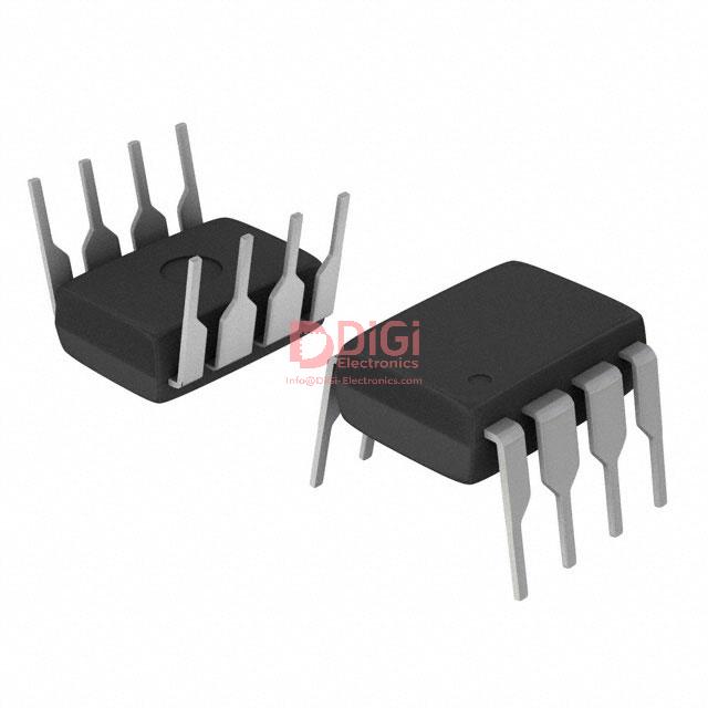
Package mechanical data of VIPER12ADIP-E
Package mechanical data for VIPER12ADIP-E centers on two primary options: DIP-8 and SO-8 packages, both engineered in alignment with STMicroelectronics’ ECOPACK® environmental policies. Precise mechanical drawings delineate all critical package dimensions, pin pitch, body width, lead thickness, and standoff heights. These specifications are instrumental for accurate PCB footprint design, directly influencing solder joint reliability, trace layout efficiency, and overall assembly quality. Variations between DIP-8’s through-hole leads and SO-8’s surface-mount gull-wing type demand differentiated land-pattern layouts and impact board-level manufacturability. For instance, SO-8 offers reduced parasitic inductance and lower thermal resistance, benefitting high-frequency switching and compact product designs, while DIP-8 supports robust mechanical retention and easier manual assembly or breadboard prototyping.
Thermal performance is closely tied to package selection and corresponding PCB design. Mechanical data such as exposed pad dimensions or lead frame geometry guides the implementation of heat spreading copper planes, via arrays, and solder coverage optimization for each package type. For SO-8, maximizing pad area beneath leads and optimizing solder paste stencil apertures can reduce thermal hotspots and enhance heat dissipation, supporting high-efficiency operation in power-dense environments. DIP-8’s bulkier leadframe may facilitate heat transfer through the leads and the PCB, but introduces challenges for automated reflow due to increased mass and differing heat sinking profiles.
Proper alignment between mechanical outlines and manufacturing constraints streamlines solderability, wetting angles, and inspection routines. Adherence to ECOPACK® criteria, inherited from the mechanical package design, ensures lead-free compatibility and aligns finished assemblies with prevailing environmental standards. It is essential during both new product introduction and sustaining engineering phases to validate that package choices are compatible with the specific solder reflow profiles, cleaning agents, and board stackups used in production lines.
Consistent reference to up-to-date package mechanical data mitigates risks of assembly defects, such as tombstoning, solder bridging, or insufficient filleting, and supports scalable DFM (Design for Manufacturability) practices. Selection of the optimal package variant for the intended application, guided by a nuanced reading of the mechanical data, secures an efficient tradeoff between electrical performance, manufacturability, and environmental stewardship. This multilayered evaluation ensures designs maintain resilience in both engineering and production workflows.
Potential equivalent/replacement models for VIPER12ADIP-E
When assessing alternatives to the VIPER12ADIP-E, it is essential to approach the evaluation by deconstructing both the functional core and the peripheral parameters that define system integration. At the heart of the VIPER12ADIP-E and similar switch-mode power supply (SMPS) controllers is the monolithic integration of a PWM controller with a high-voltage power MOSFET. This architecture streamlines offline power supply design by minimizing external component counts and delivering inherent overcurrent, overvoltage, and thermal protection mechanisms.
Close alternatives within the STMicroelectronics VIPER portfolio, such as VIPER12AS or VIPER16 series, provide a landscape of options adjustable to different design mandates. The VIPER12AS maintains a comparable electrical topology but offers distinctions in maximum drain-source voltage and packaging, while VIPER16 series introduces higher power capability and may extend operating frequency ranges. Frequency variation directly impacts transformer core selection and electromagnetic interference (EMI) design, thus requiring recalibration of associated filter networks and magnetic dimensions during migration.
Output power rating stands among the primary selection levers. VIPER12-class devices are generally suited for low- to mid-power applications, including auxiliary power modules and low-wattage AC-DC converters. Should an application demand higher efficiency or expanded load profiles, transitioning upward to the VIPER16 or exploring variants like VIPER22 series could yield better thermal margins while maintaining pin-for-pin compatibility in certain package codes.
Protection feature parity is a non-negotiable checkpoint, especially when designs must comply with stringent reliability standards. Devices with more advanced short-circuit or brownout detection circuits eliminate the need for discrete fault-handling logic, promoting board simplicity and robust field operation. It is prudent to benchmark latch-off behavior and startup sequence nuances, as subtle differences influence transient handling during brownouts or load surges, directly affecting field reliability.
Pin compatibility and PCB layout impact often become the decisive constraint in existing design updates. While package outlines may align, variations in pin function assignment or auxiliary features require careful cross-referencing of datasheet schematics. Experience has shown that mechanical fit does not guarantee electrical compatibility; detailed pin mapping and prototype validation must precede volume migration.
Progressively, there is a shift toward components with heightened integration—internal startup regulators, advanced low-power standby, and versatile enable/disable logic. Opting for such features in a replacement model can introduce future-proofing, especially where energy regulations tighten, or IoT applications require dynamic power state transitions.
Holistic selection of a VIPER12ADIP-E equivalent mandates a deliberate balance: preserving functional fidelity while exploiting incremental benefits in efficiency, reliability, and manufacturability. By systematically dissecting both the intrinsic controller architecture and the broader application context, the transition to an alternative model not only sustains system stability but often enhances resilience in the face of evolving supply-chain uncertainties.
Conclusion
The VIPER12ADIP-E from STMicroelectronics exemplifies advanced integration in offline switch mode power supply design, particularly suited for low-power applications. At the core lies its ability to handle a wide input voltage range, accommodating global grid variability and facilitating deployment in consumer and industrial environments without tethering the design to specific regional standards. This flexibility is underpinned by a current mode control topology, which not only enhances transient response and output voltage regulation but also provides deterministic overcurrent protection—critical for preventing catastrophic system failure in compact architectures.
Protection features are implemented at both circuit and system levels. The IC integrates overvoltage, overload, and thermal shutdown mechanisms, ensuring operational robustness under abnormal line or load conditions. These mechanisms function autonomously, minimizing the need for external components and simplifying the overall bill of materials. This directly impacts reliability, allowing reduction in field failure rates and maintenance overhead, particularly in demanding industrial scenarios with fluctuating load profiles.
The feedback architecture supports both optocoupler and primary-side regulation, granting design flexibility for isolated and non-isolated topologies. This adaptability enables streamlined PCB layouts and supports high-density designs often required in appliances or industrial controllers. Thermal performance benefits from DIP packaging, which offers manageable soldering and consistent mechanical stability; this facilitates both rapid prototyping and consistent production yields across multiple assembly lines.
A nuanced approach to startup requirements ensures stable power sequencing even with wide input tolerances. Designers can optimize startup resistor values and capacitance based on target inrush current profiles, preventing nuisance tripping or misoperation in complex supply hierarchies. Considering alternate part numbers can mitigate supply chain interruptions, especially for volume-driven manufacturing.
When evaluating the VIPER12ADIP-E for system integration, the alignment of protection, control, and packaging features with specific functional priorities—such as low standby consumption or high surge tolerance—often streamlines qualification processes. Its deployability across various product categories stems from a balanced engineering of both electrical performance and practical assembly traits. Design iterations leveraging this IC typically show a reduction in regulatory hurdles and production rework, translating to overall cost effectiveness and accelerated time-to-market.