 >
>


Product overview: VIPER22ADIP by STMicroelectronics
VIPER22ADIP exemplifies a tightly integrated offline switcher solution, advancing the capabilities of low-wattage SMPS configurations centered on the flyback topology. Central to its architecture is the merging of a high-voltage power MOSFET and a PWM controller within a single compact 8-DIP footprint. This integration addresses long-standing layout and reliability challenges in board design, enabling both reduced component count and minimized parasitic effects due to shorter internal connections. The fixed 60 kHz switching frequency ensures stable operation, simplifying EMI filtering requirements and allowing designers to predict frequency-related behavior with precision across applications.
The technical foundation of VIPER22ADIP elevates it beyond conventional discrete implementations. Its embedded PWM controller directly interfaces with the MOSFET gate, orchestrating robust current-mode control while providing inherent overcurrent and overvoltage protection functions. The device supports efficient start-up via an integrated high-voltage current source, eliminating the need for external bootstrap circuits and accelerating time-to-switch. During operation, the controller dynamically moderates gate drive characteristics to optimize trade-offs between switching losses and conduction efficiency, an essential feature for sustaining thermal management in tightly packed designs. Undervoltage lockout and burst-mode support further contribute to the switcher’s resilience and power-saving profile, particularly in standby or light-load scenarios.
When transitioning from the theoretical capabilities to practical deployment, several nuances become evident. In battery charger designs, the VIPER22ADIP’s capacity for precise secondary voltage regulation via optocoupler feedback is advantageous, generating stable output even under fluctuating line conditions. For TV/monitor standby rails, the device’s active clamp circuitry suppresses voltage spikes and enhances overall network longevity, mitigating stress on downstream loads. In auxiliary power units tied to motor control subsystems, the inherent noise immunity and compactness translate to improved system integration, with reduced risk of cross-domain interference during operational transients.
From a design perspective, leveraging the VIPER22ADIP involves careful optimization of transformer parameters and snubber circuits to exploit its internal protections fully. Experience shows that oversizing output filter components is unnecessary due to predictable switching harmonics and minimal device jitter at the set frequency. Thermal profiling indicates the integrated package benefits markedly from PCB copper distribution, allowing direct heat path management without additional heatsinking for most sub-20W applications. Reliability metrics improve substantially, with fewer single-point failures and a streamlined qualification process, due to the package’s factory-calibrated tolerances and comprehensive feature set.
A key observation is the way such switchers enable modular power infrastructure designs, facilitating board-level standardization. System-level diagnosability is improved by the predictable startup signature and fault feedback characteristics. The VIPER22ADIP’s deployment in digitally-controlled environments demonstrates strong compatibility with supervisory MCUs, as the tight output regulation aligns with logic-level tolerance requirements while enabling board footprint reduction—a critical driver for embedded systems targeting miniaturization and cost efficiency.
Integrating the VIPER22ADIP thus represents both an incremental enhancement to classical SMPS practice and a foundational shift toward system-centric power management approaches. The device’s configuration encapsulates performance, safety, and manufacturability in a package that promotes design reuse and accelerates time-to-market across a spectrum of compact electronic power solutions.
Key features and performance advantages of the VIPER22ADIP
The VIPER22ADIP exemplifies an integrated approach to switch-mode power supply (SMPS) design, streamlining both topology and component selection by embedding a high-voltage startup current source directly on-chip. This eliminates external high-voltage startup networks, which traditionally increase BOM costs and introduce additional points of failure—a crucial optimization in dense PCB layouts and cost-sensitive applications such as auxiliary power supplies and compact chargers. When evaluating controller selection for applications demanding universal input or variable auxiliary rails, the VIPER22ADIP’s 9V to 38V VDD operating range stands out. This wide coverage readily accommodates common supply fluctuations and brownout conditions, reducing susceptibility to undervoltage lockout (UVLO) and supporting robust operation across diverse geographical grid standards.
The adoption of current mode control architecture is another significant aspect, easing frequency compensation and facilitating inherently faster response to load transients. This architecture not only simplifies stability analysis—a persistent pain point when tuning voltage mode controllers—but also helps mitigate subharmonic oscillations in continuous conduction mode, improving predictability and electromagnetic compatibility (EMC) in demanding environments. Engineers frequently realize time savings during loop tuning, as the control-to-output transfer function’s single-pole nature is more tractable, especially for compact flyback or buck-derived topologies.
Efficiency under variable load conditions is a key performance parameter. The integrated automatic burst mode represents an effective mechanism for reducing switching frequency during light or no-load states. By adaptively minimizing switching events, it curbs core and switching losses, enabling standby power draw well below regulatory thresholds (such as those mandated by EcoDesign or DOE Level VI). This is particularly advantageous in always-on auxiliary rails for networking gear or consumer electronics, where idle power budgets are increasingly stringent. In field implementations, this feature often translates into measurable reductions in thermal footprint, further supporting compact form factors without excessive derating.
Protection suite integration is central to the device’s resilience proposition. Overload, overtemperature, and overvoltage events are addressed through autorestart logic, which not only protects the downstream circuitry but also maximizes product lifetime by preventing repeated stress cycles. The automatic recovery approach, as opposed to latching shutdown, accelerates fault clearing in noisy environments, a crucial operational advantage in industrial and white goods contexts subject to EMI spikes or mains transients.
VIPER22ADIP’s adoption in cost-sensitive, space-constrained products illustrates the value of combining such a feature-rich front end in a single package. During board bring-up and manufacturing validation, minimal external dependencies translate to shorter debug cycles and reduced points of variability, supporting both first-pass yield and long-term field reliability. Interactions with this device highlight that integrating startup, control, and comprehensive protection onto a single die often enables a margin of design resilience and manufacturability that discrete approaches simply cannot match.
In summary, effective deployment of the VIPER22ADIP centers around leveraging its system-level integration, enhanced control dynamics, and built-in protection to address the twin demands of efficiency and dependability in modern SMPS design. Applications spanning adapters, chargers, and auxiliary SMPS designs benefit from both a minimized component footprint and robust standby operation, delivering measurable engineering and commercial advantages over piecemeal solutions.
Electrical characteristics and power management
Electrical characteristics in the VIPER22ADIP are engineered to optimize both regulatory precision and robust power handling in SMPS topologies. The enforced 60 kHz fixed switching frequency establishes a stable basis for electromagnetic interference management, streamlining the design of EMI filtering stages by minimizing unpredictability in spectral emissions. This operational predictability enables tighter compliance with regulatory requirements and simpler layout strategies for designers dealing with constrained PCB real estate or harmonics mitigation at the system level.
At the core of its control architecture, the integrated current-mode PWM mechanism affords granular control over output dynamics. Fast transient response is inherent here, with the current mode feedback loop swiftly adapting to variations in input or load, minimizing overshoot and undershoot with each cycle. In practical deployment, this translates to enhanced dynamic stability under rapidly changing demand, such as in point-of-load converters for microprocessors or motor driver boards where load jumps are frequent. The internal peak drain current sensing actively tailors conduction times, maintaining switch reliability while enabling efficiency that persists across broad load profiles. This alignment between switch timing and actual load presents a balance between thermal management and conversion accuracy, reducing both stress-related failures and unnecessary power dissipation.
The output voltage-current characteristic presents a rectangular profile, a critical feature for application scenarios where distinct voltage and current thresholds are mandatory. In battery charging infrastructure, the ability to govern both constant-voltage and constant-current stages ensures safe and fast charging cycles while mitigating risks of cell degradation. Implementing the VIPER22ADIP together with an adaptive feedback circuit such as the TSM101 enables precise transition between charging phases, fulfilling the dual objectives of maximum charge rate and full-cycle protection. The underlying mechanism extends beyond basic regulation; it establishes a platform for finely-tuned power delivery adaptable through external sensing, reflecting practical experiences where maximizing charge throughput without overheating is required.
Wide tolerance at the VDD pin facilitates direct interface to auxiliary windings, broadening startup conditions and enhancing reliability under varying input voltages typical in grid-tied or universal input supplies. This configuration removes the necessity for cumbersome startup components and accelerates power-on sequences—a key advantage in systems where quick boot times are paramount. The design also confers immunity to brownout scenarios, maintaining control logic integrity over a large operating envelope.
Overall, high integration and a focus on precise, adaptable power management enable this device to act as a versatile, application-driven switch-mode controller. The layered control structure, from hardware-based current regulation through intelligent output profiling and advanced startup features, directly supports differentiated SMPS implementations, including compact chargers, auxiliary AC/DC modules, and high-reliability industrial supplies. This approach underscores the importance of embedding flexible power management strategies within the device, pushing forward the optimization of converter efficiency, system protection, and design simplicity.
Application-specific design considerations for the VIPER22ADIP
Application-specific design of circuits using the VIPER22ADIP centers on its unique current-sensing feedback architecture. Unlike traditional voltage-mode feedback, the dedicated feedback pin on the VIPER22ADIP measures primary-side current, enabling precise modulation of the internal switching MOSFET. This method enhances loop response speed and accuracy, especially when combined with an optocoupler-based secondary-side feedback loop. Designers can leverage this architecture to strengthen dynamic regulation in isolated power supplies, ensuring stable output across a broad range of loads while reducing sensitivity to transformer tolerances and PCB layout variations. Robust feedback implementation translates directly to improved EMC performance and output quality, making the device effective for demanding industrial or medical applications where regulatory compliance is mandatory.
Startup behavior is governed primarily by the sizing of the VDD supply capacitor. The capacitor must provide an energy reservoir sufficient for the device’s controller during the initial power-up sequence, prior to the auxiliary winding energizing the VDD rail. An undersized capacitor frequently results in startup hiccups or lockout, disrupting normal operation and potentially initiating repeated inrush surges. Conversely, over-sizing the capacitor unnecessarily increases system cost and startup delay. Empirical experience points to calculating the worst-case energy requirement based on switching frequency, control circuitry consumption, and transformer saturation characteristics. This approach ensures the VIPER22ADIP transitions seamlessly into steady-state operation, minimizing stress on the auxiliary bias components.
The VIPER22ADIP’s rectangular output mode directly facilitates integration into multi-phase charging profiles, typical in Li-ion battery management systems. This output characteristic supports consistent current-limited and voltage-limited operation, enabling simple implementation of charge algorithms without the need for external, complex analog control loops. It provides streamlined safety management, as the device inherently limits both the peak current and the output voltage, reducing the risk of thermal stress or overcharge scenarios. Practical deployments demonstrate marked improvements in battery lifecycle and charging efficiency compared to disparate discrete design methods, underlining the benefit of the integrated approach for consumer and portable industrial applications.
Burst mode operation represents a key differentiator in energy-sensitive designs such as standby power supplies and adapters. By introducing periodic pauses in switching at light loads, the VIPER22ADIP minimizes core losses in the transformer and the conduction losses in the power MOSFET. This approach drastically reduces no-load power consumption, ensuring compliance with tightening regulatory standards for standby efficiency. The inherent controlled burst timing and soft-restart mechanisms embedded in the controller prevent audible noise generation and mitigate transformer magnetostriction effects, challenges often encountered in other burst-mode designs. Field measurements reveal lower component temperatures and extended mean time between failures, substantiating the device’s suitability for high-reliability applications.
In application, optimal results are achieved by viewing the VIPER22ADIP as a highly integrated power management solution, rather than a simple offline flyback controller. Careful alignment of feedback network design, startup capacitor sizing, output mode selection, and burst mode enablement yields performance that meets advanced requirements for efficiency, safety, and longevity in both consumer electronics and industrial infrastructure. These design considerations not only improve technical metrics but also simplify regulatory certification pathways and reduce total cost of ownership.
Start-up, protection, and reliability features in VIPER22ADIP
The VIPER22ADIP power IC implements a suite of tightly integrated start-up, protection, and reliability mechanisms architected for robust converter operation across demanding applications. At the core, the high-voltage startup current source activates directly from the primary input rail, eliminating external components typically required for cold-start routines. This direct high-voltage initiation streamlines PCB design, reduces part count, and minimizes fault exposure at initial power-up stages, providing an immediate boost in hardware dependability and maintenance simplicity.
Layered within the power management subsystem, the auxiliary undervoltage lockout (UVLO) circuit employs precision hysteresis to maintain operational margins. By monitoring supply rails for voltages below critical thresholds and inhibiting switching functions in compromised scenarios, unintended turn-on events are effectively blocked. The incorporation of hysteresis ensures that recovery from brown-out or transient voltage dips proceeds in a controlled manner, averting oscillatory behavior and false triggering—an approach validated in multi-mode converter setups where supply stability varies under load steps.
Further reinforcing the system, the overvoltage protection mechanism anchors itself to the VDD pin via an integrated monitoring detector. Upon detecting excursions above predetermined limits, the device engages self-reset protocols after the fault clears, maintaining system responsiveness. Unlike hard-latch architectures, the auto-reset topology offers immunity to single-event upsets, decreasing downtime and eliminating the need for manual intervention during recoverable faults. This proves advantageous in compact supply layouts where physical access is restricted and continuous regulation is crucial.
The current and thermal protection modules employ auto-restart features contextualized for adversarial operating conditions. When excessive current flow or temperature spikes are detected, controlled shutdown is automatically followed by periodic restart attempts, striking a balance between protection and availability. This cycle assures continued functionality in environments characterized by intermittent faults, such as those found in industrial plant controls or variable ambient conditions, where overstress events are sporadic but brief. Real-world deployment demonstrates fewer service interruptions compared to systems with static failure shutdowns.
Temperature shutdown monitoring operates transparently to safeguard components against thermal runaways. By continuously surveilling die temperature, the device reacts preemptively to overloads, ceasing operation just prior to critical limits and resuming when thermal equilibrium returns. In practice, this results in sustained service life and higher tolerance against unpredictable cooling scenarios or enclosure hot spots.
From an engineering perspective, the synergy between proactive protection circuits, auto-restart logic, and responsive start-up subsystems tightly converges on reliability. When applied to mission-critical applications—such as power modules in networked automation, LED drivers, or consumer electronics—the hierarchical approach to fault detection, isolation, and recovery maximizes uptime. Experience indicates that embedding these layered mechanisms within primary-side control architectures typically results in lower field failure rates and more predictable performance across diverse operating profiles. The VIPER22ADIP achieves this by blending rapid activation, intelligent monitoring, and adaptive protective responses, producing a robust power conversion backbone suitable for both new and legacy design environments.
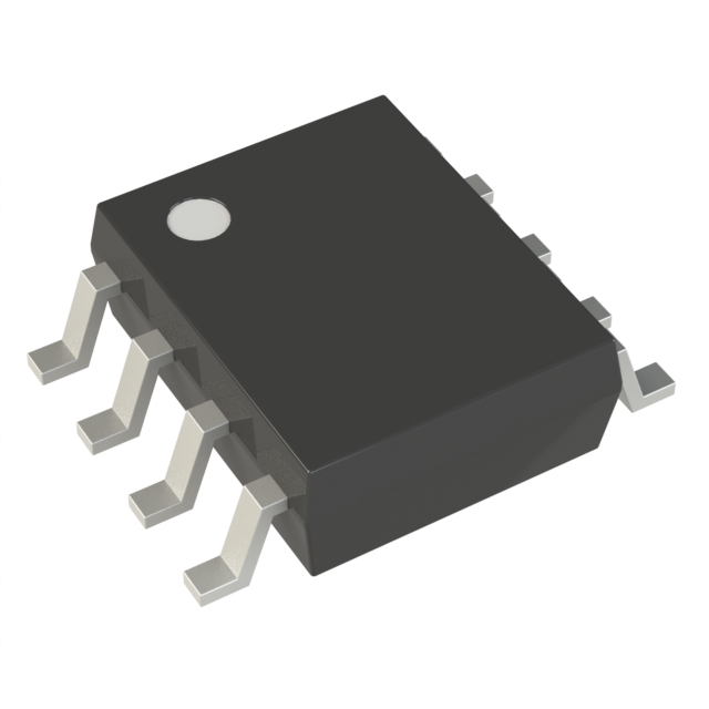
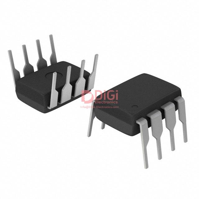
Mechanical and packaging attributes of the VIPER22ADIP
Mechanical and packaging attributes of the VIPER22ADIP demand close attention due to their direct influence on assembly efficiency, mechanical integrity, and thermal performance. The device leverages the industry-standard 8-DIP (dual in-line package), a choice driven by both functional advantage and ecosystem compatibility.
Central to the 8-DIP format is its universality across traditional through-hole assembly techniques. This ensures optimal fit with a broad array of legacy and current manufacturing lines, avoiding the need for custom fixtures or specialized handling. The regular pin spacing and parallel lead geometry minimize the risk of solder bridging and misalignment, key factors in sustaining high yield rates during wave soldering or manual insertion cycles. Given the consistent dimensions, automated pick-and-place systems, as well as hand assembly, can process the component interchangeably, supporting flexible manufacturing scenarios where product configuration may change with minimal retooling.
Durability is reinforced by the mechanical design of the DIP body. Molded with rigid thermoset epoxy, the package offers resistance to common stresses encountered during board handling, probing, or repetitive insertion/removal operations. The robust pin-lead structure ensures secure engagement with both soldered footprints and traditional IC sockets, aiding prototyping and field-swappable module requirements. The package-side chamfers and notch further serve as tactile and visual alignment guides, reducing assembly errors and expediting troubleshooting workflows.
Available dimensional and mechanical data serve as critical inputs for PCB and enclosure engineering. These standardized drawings streamline mechanical-CAD to ECAD integration, providing an unambiguous basis for component land-pattern development, trace-clearance planning, and height stacking in dense assemblies. The predictable thermal resistance profiles associated with the 8-DIP package facilitate straightforward power-dissipation calculations, enabling designers to quickly check junction temperature margins against worst-case loading. Practical test setups reflect this: thermal probes mount readily to DIP packages, and air convection around the device remains reliable, even in compact PSU or control board layouts.
Broad application experience highlights a key operational advantage: the DIP form factor tolerates higher insertion and extraction cycles with lower risk of lead fatigue compared to surface-mount options under similar stress levels. This feature is frequently leveraged in field-serviceable applications or environments prone to vibration-induced micro-movement, where solder joint mechanical robustness can be a limiting factor. In densely populated boards, the linear footprint of the VIPER22ADIP allows straightforward signal routing and debugging access, supporting iterative board rework without significant layout compromise.
A core insight arises from the intersection of design simplicity and ecosystem compatibility. While more modern low-profile packaging offers greater density, the 8-DIP remains unmatched for ease of prototyping, rework, and legacy support—attributes that often drive initial platform success and sustain long-term reliability in demanding power applications. For designers requiring rapid proof of concept, in-circuit adjustment, or robust socketed design, the VIPER22ADIP’s mechanical package consistently bridges the gap between field pragmatism and manufacturing efficiency.
Potential equivalent/replacement models for the VIPER22ADIP
Selecting an appropriate replacement for the VIPER22ADIP hinges on a clear understanding of the device's internal architecture and electrical characteristics. At its core, the VIPER22ADIP integrates a high-voltage power MOSFET and control circuitry optimized for off-line power conversion. Key functional blocks, such as integrated current-mode PWM control, under-voltage lockout, and overload protection, contribute to robust operation in compact switch-mode power supply designs. When seeking an alternative, devices like the VIPer22AS deserve focused examination, as they leverage the same topological choices and protection schemes, ensuring largely seamless migration in many design flows.
The VIPer22AS distinguishes itself with comparable input voltage ranges, switching frequencies, and integrated protection features. Its pin configuration and package outline closely align with those of the VIPER22ADIP, streamlining PCB layout adaptation. However, nuanced differences such as maximum drain-source voltage, output power limits, and start-up current profiles may arise. These parameters, while similar, necessitate thorough scrutiny in applications demanding strict compliance to original specifications, especially in thermally constrained or high-efficiency scenarios. Direct device substitution without examining such variations might compromise reliability or regulatory compliance, particularly in industrial or consumer product certifications that reference specific silicon revisions or datasheet guarantees.
During practical deployments, variations in thermal performance between DIP and other package types have revealed trade-offs in heat dissipation and mechanical robustness. Designers regularly encounter constraints imposed by vertical space, soldering processes, and cooling methods, all of which must be accounted for when swapping between models or package variants. Experience shows that reviewing not only the headline electrical ratings but also the detailed switching behavior and EMI characteristics can forestall debugging cycles later in development. Device qualification labs typically require side-by-side testing under worst-case operating conditions to validate compatibility, with attention to soft-start timing and short-circuit response.
When circuit topology or footprint constraints dictate the need for alternatives, leveraging design houses’ application notes and reference designs enables efficient risk mitigation. However, a core insight is that direct equivalency rarely transcends a simple parameter checklist; holistic model evaluation, including simulation of transient response and long-term durability, substantially reduces field failure risks. Insights emerging from iterative prototyping suggest that the subtle behavioral differences between alternatives can manifest under high crest factor load conditions or during brown-out events, highlighting the importance of simulation-driven selection rather than mere datasheet comparison.
Ultimately, the process of substituting the VIPER22ADIP extends beyond matching electrical parameters—it requires a layered investigation of packaging, control characteristics, and operating margins, coupled with rigorous empirical validation to realize stable, manufacturable designs that meet specification without sacrificing manufacturability or compliance. This multidimensional approach ensures that chosen alternatives perform equivalently not only in nominal scenarios but across the full spectrum of real-world operating conditions.
Conclusion
The VIPER22ADIP from STMicroelectronics consolidates high-voltage startup circuitry, PWM controller, and MOSFET into a single, space-efficient package that streamlines flyback SMPS architecture. Central to its design is current-mode control, which enhances loop stability and transient response. This method improves load regulation and mitigates the risk of subharmonic oscillation, directly benefiting applications where input voltage can vary widely or rapid load changes are common. Integration of such control significantly constrains component count, reducing layout complexity and facilitating adherence to EMI regulations.
In operational environments, the device’s robust protection functions—including overload, over-temperature, overvoltage, and short-circuit safeguards—directly reinforce long-term system reliability. These mechanisms autonomously handle fault scenarios, minimizing the risk of catastrophic failure and simplifying the protection design burden. This is especially critical when designing auxiliary power supplies for industrial or consumer electronics, where downtime or recalls are costly and rapid diagnostic clarity is essential.
The ease of integration into design workflows is evident in the consistent electrical characteristics, straightforward feedback configuration, and support for primary-side regulation. These features enable rapid prototyping and streamline the qualification process. The DIP package not only aligns with conventional through-hole assembly lines but also provides long-term mechanical robustness, accommodating vibration or thermal stress found in real-world installations. Compatibility with drop-in alternatives further de-risks supply chain disruptions, a frequent concern for procurement teams in volatile component markets.
Experience from field deployments confirms that leveraging the VIPER22ADIP results in lower BOM cost and smaller PCB footprint while sustaining efficiency across wide input ranges. For battery charging and AC-DC auxiliary rails, its self-supply architecture and low standby power cater to modern regulatory standards on energy consumption. The component’s comprehensive integration refocuses engineering effort from basic power stage realization towards system-level differentiation—such as advanced supervisory, monitoring, or connectivity functions.
Adoption of VIPER22ADIP in diverse deployments reveals a consistent pattern: the device’s blend of electrical resilience, design flexibility, and supply assurance provides genuine competitive advantage. Its architecture embodies a mature, component-level response to the evolving demands of power electronics—favoring modularity, rapid adaptation, and lifecycle endurance necessary for next-generation power conversion systems.