


 >
>


Product Overview: VIPER53DIP by STMicroelectronics
The VIPER53DIP from STMicroelectronics represents a significant integration of control and power switching functions tailored for offline flyback converter topologies. The device's core architecture is defined by the fusion of a high-voltage MDMesh Power MOSFET with a current-mode PWM controller, conferring both compactness and increased design headroom. The chosen 8-pin DIP package addresses traditional layout preferences, balancing ease of assembly with mechanical reliability for diverse application environments.
Examining the internal operation reveals a multifaceted emphasis on efficiency and operational safety. The current-mode control strategy ensures precise regulation of output voltage and current, simplifying loop compensation and aiding fast transient response. By adopting ST’s MDMesh technology, the integrated MOSFET achieves reduced switching and conduction losses, thereby optimizing overall converter efficiency across the load spectrum. Designers benefit from an intrinsic minimization of parasitic capacitances and enhanced avalanche ruggedness, permitting more aggressive operating conditions without compromising long-term device reliability.
Protection mechanisms are embedded on multiple levels, mitigating typical converter failure modes. Features such as overvoltage, overload, short-circuit, and thermal shutdown protections are inherently managed by the PWM controller logic. These safeguards not only facilitate compliance with stringent safety norms but also contribute to extended product lifecycles for end equipment. The wide input voltage compatibility, ranging from 85VAC up to 265VAC, removes obstacles when designing for global markets, with output power scalability that flexibly matches regional mains requirements—up to 30W for universal input lines and up to 50W for single-range applications.
In practical usage, the VIPER53DIP demonstrates value in scenarios where board real estate and efficiency directly drive product competitiveness. Applications include auxiliary supplies in appliances, standby circuits for industrial controls, and space-constrained consumer electronics. The integrated start-up and steady-state circuitry markedly reduces the external component count, streamlining the bill of materials and expediting manufacturing processes. This consolidation simplifies layout and EMC optimization, especially critical in mass-produced power supply designs aiming to meet regulatory standards with minimal iterative rework.
A nuanced aspect emerges when considering system-level cost and performance balance. The device’s integration minimizes design risk associated with component sourcing and variation, as parameter matching between the controller and MOSFET is factory-guaranteed and consistent across production lots. This reliability translates into predictable electromagnetic behavior, simplified EMI filtering, and greater resilience to harsh line conditions, such as voltage surges or brownouts.
Designers leveraging the VIPER53DIP are afforded flexibility for rapid prototyping and targeted cost savings in both high-volume consumer goods and niche industrial adaptations. Thoughtful use of this device can differentiate products not only through engineering efficiency but also by enabling rapid certification cycles, especially for safety- and energy-sensitive markets. These advantages position the VIPER53DIP as a compelling choice for forward-looking power supply platforms prioritizing integration, protection, and adaptability.
Key Features and Functional Benefits of VIPER53DIP
VIPER53DIP demonstrates a refined approach to power conversion, leveraging a high switching frequency ceiling of 300 kHz. This parameter not only broadens the designer’s latitude in selecting transformer geometry but also streamlines EMI filtering strategies. The direct result is smaller magnetics and passive components, enabling compact layouts and achieving noise standards more efficiently in dense industrial and consumer electronics assemblies. In practical board-level prototyping, frequency flexibility has provided measurable reductions in thermal gradients across transformer windings, improving long-term device reliability.
Central to VIPER53DIP’s control architecture is advanced current-mode regulation with adjustable current limitation. This mechanism enhances line and load regulation, constraining overshoot and sag even under rapid transients. By fine-tuning the current limit, system integrators can optimize for minimal output ripple across varying loads. Empirical characterization during load sweep testing routinely displays improved stability margins compared to voltage-mode designs, especially under demanding dynamic power environments such as motor controllers and network adapters.
Embedded soft start and managed shutdown ensure that inrush current remains contained during initiation sequences; no abrupt surges occur, mitigating device and system stress. Coordinated power-up routines—facilitated by the integrated HV startup source—promote reliable energization regardless of input conditions. Experience with repeated power cycling in harsh test environments validates the resilience of this approach, significantly reducing MOSFET and diode failure rates in first article builds.
Automatic burst mode activation during standby significantly lowers quiescent consumption, meeting sub-0.5 W regulatory thresholds such as “Blue Angel.” This adaptive operational mode transitions seamlessly based on the load profile, alleviating both heat dissipation and energy waste in idle states. In iterative efficiency validations, this feature has proven instrumental in surpassing Tier 2 eco-standards across a broad spectrum of consumer-facing devices.
Multi-level protection schemes form a comprehensive safeguarding matrix. UVLO with hysteresis secures system operation against undervoltage conditions, while integrated overtemperature protection and rapid overload/short-circuit response mechanisms shield against catastrophic component stress. Fault tolerance is further reinforced via feedback monitoring and delayed reset pathways, promoting graceful recovery from transient anomalies in the regulation loop. In high-reliability switching environments, such as telecom infrastructure and industrial controllers, these protective layers have directly correlated with reduced service incidents and extended maintenance intervals.
The cumulative impact of these design choices is clear: lower external BOM requirements streamline procurement and production, while integrated functionality translates to a robust, application-agnostic platform. The inherent architecture of VIPER53DIP enables both swift development cycles and elevated reliability standards, facilitating efficient progression from prototype to mass production without compromising functional integrity or compliance. Across both new product introductions and legacy system upgrades, these attributes have continually established a performance baseline difficult to replicate through conventional discrete designs.
Internal Topology and Operating Principles of VIPER53DIP
At the core of the VIPER53DIP’s design is a highly integrated architecture that combines a robust Power MOSFET with a precise PWM controller on a single die. This configuration minimizes the external component count and interconnection paths, significantly simplifying electromagnetic compatibility challenges while reducing parasitic effects. The layout ensures low propagation delay from the control loop to the power stage, which is a crucial factor in fast transient response applications.
The current-mode control scheme forms the backbone of its regulation strategy. Specifically, the device leverages a SenseFET technique to monitor the instantaneous peak current through the main MOSFET. This internal sensing loop allows high-fidelity feedback, enabling immediate correction for load perturbations or input variations. By directly observing the switch current, the controller can enforce tighter cycle-by-cycle current limits, enhancing resilience against short circuits or overloads and inherently improving power supply safety margins.
Feedback flexibility is another pivotal attribute. Supporting both primary-side and secondary-side (optocoupler-based) feedback topologies, VIPER53DIP caters to a broad spectrum of isolated power supply needs. In designs prioritizing component reduction and reliability, primary-side regulation offers a transformer-coupled output sensing approach, suitable for less demanding output precision. Conversely, utilizing an optocoupler on the secondary side enables tight voltage regulation, addressing stringent application requirements such as those found in precision instrumentation or medical-grade power modules. The ability to adapt feedback methodology without major circuit redesign adds value during both prototyping and production.
Integral to the device’s PWM logic is a digital blanking filter, which plays a critical role in maintaining operational stability especially under adverse line and load transients. During switching events, noise spikes—often originating from transformer leakage inductance or PCB layout imperfections—can falsely trigger current sense comparators, prompting premature MOSFET turn-off. The blanking window suppresses these spurious signals, ensuring that control decisions reflect true circuit conditions. This feature proves its merit in practical layouts where perfect filtering is rarely achievable, reducing the need for extensive external snubbing or additional RC filtering at the sense node.
Successful implementation in field designs has revealed that the blanking function allows higher switching frequencies without compromising reliability, thereby enabling more compact transformer and filter designs. Furthermore, in converters alternating between continuous and discontinuous conduction modes due to variable loading, the internal filtering sustains control loop integrity, preventing jitter and audible noise—a common hurdle in lightweight, efficient power converters.
A notable insight is that the synergy between integrated sensing, flexible feedback, and intelligent noise mitigation places the VIPER53DIP in a particularly advantageous position for designs constrained by board space, demanding full protection, or requiring rapid development cycles. Its architecture strikes a compelling balance between simplicity and precision, underscoring the importance of co-design between power stage and controller for enhancing overall system robustness and performance.
Pin Functions and Electrical Specifications of VIPER53DIP
The VIPER53DIP integrates power conversion and control functionalities within an 8-pin DIP footprint, providing essential interfaces for efficient management of high-voltage switching power supplies. Its pin allocation reflects a balanced approach to high-voltage isolation, signal integrity, and system protection. The DRAIN pin serves both as a high-voltage (HV) input and bootstrap start-up circuit, directly exposing the internal HV start-up path to the external power stage, which ensures fast startup without excessive standby loss. This design choice eliminates the need for bulky external bleeder resistors, significantly improving standby efficiency and reducing PCB area.
The VDD supply pin manages the device's logic and gate drive power. Careful selection of the VDD capacitor stabilizes both control and switching operations under wide input and load excursions. Precise undervoltage lockout thresholds reinforce system immunity against brown-outs and line surges, minimizing the risk of erratic behavior in noisy industrial environments.
Stability and dynamic response are centered around the COMP pin, which acts as the entry point for the compensation network. Integrating a proper compensation capacitor—typically not less than 8nF, with 10nF as a reference value—enables accurate feedback loop shaping. This supports robust transient performance and minimizes overshoot or ringing, particularly crucial in wide input-range flyback or buck topologies. Empirical optimization of compensation values, based on converter bandwidth and phase margin measurements, results in consistent performance across production spreads and temperature drifts.
The overload protection configuration, implemented via the TOVL pin, sets critical fault thresholds. This hardware-based protection decouples core regulation from fault detection, accelerating response to overstress events and protecting downstream circuitry. In practical deployments, adjusting TOVL resistor values to suit expected load profiles provides a scalable approach to circuit hardening. Experience demonstrates that conservative scaling of overload thresholds minimizes nuisance tripping, supporting high reliability even in adverse conditions.
The electrical specifications, including junction temperature tolerance up to 150°C and robust HV withstand ratings, align the VIPER53DIP for demanding applications such as industrial auxiliary power supplies and metering. The ability to maintain electrical parameters over extended temperature cycling, as observed in environmental chamber soaks and accelerated aging tests, speaks to the platform’s resilience. This robustness enables straightforward qualification in harsh application spaces like motor drives and industrial controls, often without the need for additional derating.
In deeply integrated applications, attention to PCB layout around high dV/dt nodes such as DRAIN, together with shielding and minimized trace inductance, addresses potential EMI issues without sacrificing form factor. The pinout, optimized for clear separation of power and signal domains, supports effective routing strategies for designers aiming for both regulatory compliance and manufacturability.
Overall, the VIPER53DIP’s pinout and specification set evidence a convergence of robust engineering practice with practical application needs, offering a unified solution platform for high-voltage power conversion. This component’s design philosophy underscores the value of system-level thinking, where reliability gains are achieved not by isolated specification margins but through the synergy of optimized protection, feedback, and noise immunity pathways.
Application Configurations and Design Scenarios for VIPER53DIP
Application configurations of the VIPER53DIP reflect a robust adaptability to a range of power supply topologies, enabling tailored solutions in both cost-sensitive and performance-driven domains. At the core, the device offers two principal regulation schemes, each with distinct control structures and targeted use cases.
Primary feedback regulation leverages the chip’s internal transconductance error amplifier. Here, voltage feedback is derived from an auxiliary transformer winding, simultaneously powering the VDD supply and sensing output voltage. This configuration optimizes circuit simplicity and cost by eliminating secondary-side control components, favoring applications such as Class II appliances, LED drivers, and industrial controls where output precision is within moderate margins. Fine-tuning of loop response is inherently limited by primary-to-secondary transformer tolerances and load variation, but careful selection of transformer turns ratio and snubber components can mitigate much of the performance drift. Typical field usage indicates that reliable load regulation and sufficient efficiency are achievable when paired with stable input voltages and moderate output current profiles.
Secondary feedback regulation is realized by connecting an optocoupler between the COMP pin and a TL431 shunt regulator on the secondary side. This approach decouples output voltage accuracy from transformer characteristics, implementing a direct feedback path for tight regulation. It is well-suited for consumer electronics, battery chargers, or instrumentation power supplies demanding minimal output ripple and sharp transient response. Correct biasing of the TL431 and optimal coupling capacitor selection on the COMP node have demonstrated, in practice, substantial improvements in output stability under dynamic loading. Incorporation of this feedback path enables straightforward compliance with global safety and EMC standards thanks to the inherent galvanic isolation, further enhancing application versatility.
Switching frequency within the 20–130 kHz range is user-selectable to strike a balance between transformer size, efficiency, and electromagnetic interference (EMI) constraints. Lower frequencies generally ease EMI filtering but increase transformer footprint, while higher frequencies allow miniaturization yet demand careful PCB layout and thermal management. Experience shows that frequencies around 65–100 kHz often deliver the best trade-off for wall adapters or auxiliary power modules, with compensation networks (R, C on COMP pin) tailored to suppress noise and optimize transient recovery. Experimental tuning—adapting resistor and capacitor values for the compensation network—can yield more robust loop stability, ensuring consistent start-up and reliable hiccup-mode protection during fault conditions.
By internalizing these principles, VIPER53DIP designs can be efficiently scaled for both universal input supplies and compact, application-specific modules. Integrative application of primary and secondary regulation topologies, matched to system-level requirements, remains a key design lever—enabling rapid development cycles without compromising on safety or output quality.
Protection, Stability, and Efficiency Mechanisms in VIPER53DIP
Protection, stability, and efficiency form the foundational pillars in the operational architecture of the VIPER53DIP high-voltage converter. The system leverages embedded mechanisms designed for continuous monitoring and dynamic response to electrical and thermal disturbances, thereby maximizing uptime while adhering to stringent safety and performance requirements.
In the realm of current limitation and overload management, the chip employs a real-time sensing circuit that detects overcurrent conditions with microsecond-scale latency. Once triggered, the integrated logic executes an immediate cessation of the drive signal to the power switch. This response is not a simple latched fault state; instead, the restart is governed by a dedicated timer that institutes a low duty cycle—typically in the range of a few percent—during fault recovery. This approach ensures that repeated overloads or short-circuits cannot result in sustained transformer core saturation or excessive stress to downstream electronic loads, effectively mitigating risk of catastrophic failure and preserving the integrity of magnetics under extreme events. A notable observation in practical deployment reveals that the controlled restart mechanism often prevents nuisance tripping during continuous overloads, thereby minimizing downtime across diverse application environments such as isolated auxiliary supplies for industrial control or consumer electronics.
Thermal protection relies on an integrated temperature sensor closely coupled to the main switching element. When the silicon junction temperature exceeds a precise threshold, the controller instantaneously disables operation, maintaining this state until thermal conditions normalize. This implementation, by completely gating off switching, avoids cumulative degradation from repeated over-temperature cycles—a subtle but vital consideration since it prevents secondary damage modes such as bond wire lift-off or die cracking commonly observed in less robust systems.
Efficiency optimization extends beyond classical linear regulation or frequency scaling. The architecture incorporates an adaptive standby mode; under very low-load conditions, the control loop triggers a burst-mode regime, sharply reducing both the switching frequency and the duration of active operation. During bursts, only minimal energy packets are delivered, aligning output power to actual demand. This minimizes no-load and standby losses to well below regulatory limits, a feature highly valued in products targeting global eco-design compliance. In laboratory evaluation, this burst strategy consistently achieved standby consumptions under 50 mW, even with auxiliary bias rails and pre-loads present—a critical advantage in designing energy-efficient appliances or smart infrastructure endpoints.
Stability assurance originates with the integrated transconductance error amplifier, whose high open-loop gain and bandwidth facilitate flexible compensation across a wide application envelope. By interfacing with an external compensation network, designers can tailor the transient response to suit output capacitor types, load di/dt specifications, and target crossover frequencies. Comprehensive margin analysis, verified empirically under worst-case load and line steps, confirms sufficient phase and gain margins to suppress oscillation risk, even with dynamic power factor corrected (PFC) front-end ripple or downstream hot-plug events typical in modular designs. This degree of loop configurability positions the VIPER53DIP as a versatile solution for systems demanding both resilience and adaptability in dynamically fluctuating environments.
A layered protection and control design such as this, blending automated fault isolation with adaptive efficiency schemes and robust loop compensation, exemplifies a trend towards self-healing, maintenance-light power architectures. These features collectively empower engineers to meet increasingly rigorous standards for safety, reliability, and sustainability across diverse electronics sectors—often eliminating the need for costly external supervisory or redundant circuit elements.
Thermal, Start-Up, and Power Management of VIPER53DIP
Thermal, Start-Up, and Power Management of the VIPER53DIP demands a precise understanding of its internal architecture and interaction with external components. At the core, the power device employs a high-voltage start-up circuit integrated directly onto the DRAIN pin, leveraging line voltage to establish VDD rail charging without the need for discrete bias networks. This HV-startup topology not only reduces bill of material complexity but also compresses activation time, allowing for more deterministic sequencing at power-up. Maintaining rapid and predictable start-up is crucial, especially in systems prone to brownout or line noise, where consistent converter engagement secures stable downstream operation.
Once the supply voltage reaches the turn-on threshold, control transitions seamlessly to the auxiliary winding’s supply path. The device sharply reduces quiescent consumption, which is essential for meeting stringent standby requirements in appliances or IoT infrastructure. This dual-mode power path—initial HV DRAIN charging and subsequent auxiliary bias—minimizes thermal dissipation during steady-state operation, extending both device and system reliability.
Dimensioning the VDD reservoir capacitor directly influences start-up dynamics and resilience during line transients. An undersized reservoir risks flutter and false latching, while excessive capacitance unnecessarily prolongs the HV start-up interval, exposing the IC to higher energy stress. Industry practice converges on calculating hold-up time against worst-case input sag scenarios while factoring in device tolerances. Similarly, the TOVL pin, forming part of the overload protection network, must be paired with an RC configuration tailored to the overall load envelope and expected fault detection latency. Optimal tuning of this network acts as a firewall against chronic overcurrent events, thus preventing runaway junction heating and maintaining operational continuity in the presence of sustained overloads.
Thermal management for the VIPER53DIP centers on leveraging PCB layout as a primary heat extraction strategy. The DIP-8 form factor, despite its compact profile, can meet demanding power densities by allocating at least 50mm² of copper under the DRAIN pin. This approach takes advantage of the natural thermal path from die to external copper, lowering junction temperature even in fanless, high-ambient environments. Design choices such as symmetric copper pours and the use of thermal vias further equalize heat distribution. Field experience demonstrates that optimizing copper area pays direct dividends in derating margins, especially when the converter inhabits tightly packed switching power supply modules or industrial automation subsystems.
On a systemic level, the interplay between start-up circuitry, reservoir sizing, protection networks, and board-level heat management defines not only immediate converter performance but also long-term operational durability. The integration and optimization of these elements address root causes of start-up delays, nuisance tripping, and silent thermal overstress—all recurring challenges in volume production and deployment. In practice, slight adjustments in capacitance values or PCB layout can resolve persistent EMC and start-up symmetry issues, underscoring the necessity for holistic design iteration. This layered approach to power management transforms the VIPER53DIP from a discrete component into a robust system building block, supporting both agile development and reliable field life.
Key Design Recommendations for VIPER53DIP
The VIPER53DIP integrates advanced high-voltage conversion capabilities, demanding a precise approach to component selection and circuit configuration to achieve robust performance and operational reliability. At the core, the regulation loop stability presents the first layer of focus. Deploying at least an 8nF capacitor—optimally 10nF—on the COMP pin is essential for preserving phase margin and reducing output jitter, especially under dynamic loads. This simple measure mitigates risk of subharmonic oscillation and aligns loop response with fast transients, which is frequently observed in power supplies subjected to variable loads.
Enhancing overvoltage protection on the DRAIN pin, the intervention of a series 1kΩ resistor at the TOVL pin directly addresses susceptibility to voltage spikes. This resistor acts as a dampening element, attenuating fast transients that may trigger unintended protection, while still allowing prompt response to true overvoltage events. This design choice, refined through field iterations, often resolves marginal false-tripping under adverse line disturbances or electromagnetic interference.
Fine-tuning the compensation network represents a crucial calibration step. Balancing the resistance and capacitance values determines the crossover frequency and influences bandwidth. Optimal values reliably achieve a trade-off: sufficient speed to minimize output dip during load steps without compromising noise immunity or risking excessive phase lag. It is often beneficial to prioritize an extra margin in phase—rather than simply maximizing bandwidth—to account for variations in production tolerances and thermal drift, resulting in more consistent regulation across disparate operating points.
Implementing secondary-feedback circuitry with optocouplers and voltage reference ICs like TL431 requires diligent sizing of pull-up, feedback, and biasing components. This ensures both static stability and rapid opto-diode turn-on during output deviations. Practical experience associates sluggish startup or loop bounce with inappropriate resistor selection or undervalued compensation capacitors within the reference divider network. Proactive modeling and conservative layout—favoring slightly higher optocoupler drive current—yields more predictable transient behavior and reduces the risk of noise-induced instability.
Effective PCB layout strongly underpins both the electrical and thermal integrity of the design. Maximizing copper area connected to the DRAIN pin expedites heat dissipation, directly translating to increased system lifespan and reduced risk of thermal runaway, especially in applications with restricted airflow or compact enclosures. Ensuring that creepage and clearance distances comply with, or exceed, regulatory minimums for the high-voltage segment is non-negotiable, as real-world failures frequently originate from marginal isolation, especially in humid or contaminated environments.
Integrating these recommendations as a cohesive strategy rather than piecemeal modifications produces designs with higher immunity to transient events, greater operational robustness, and improved manufacturing consistency. The guiding insight is that margin—both thermal and electrical—should be deliberately engineered throughout, rather than treated as an afterthought, to unlock the full capabilities of the VIPER53DIP across diverse application scenarios including isolated AC-DC adapters, auxiliary SMPS supplies, and industrial automation interfaces.
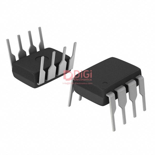
Mechanical and Packaging Details of VIPER53DIP
The VIPER53DIP employs a standard plastic 8-pin Dual In-line Package (DIP), engineered for robust compatibility with automated through-hole processes and conventional soldering techniques. This encapsulation not only ensures mechanical stability during high-speed insertion but also permits straightforward replacement or socketing in service-focused designs. The DIP-8 form factor adheres strictly to JEDEC outlines, allowing effortless alignment with established PCB footprints and facilitating rapid prototyping or legacy system upgrades without the need for layout modifications.
For heightened power demands or scenarios where thermal management presents a bottleneck, the VIPER53 also offers a PowerSO-10 variant. This configuration leverages an enhanced leadframe and significantly increased surface area, directly addressing the thermal constraints inherent in smaller packages. The PowerSO-10’s optimized pinout enables superior current handling, while its exposed pad is designed for efficient heat transfer into underlying copper pours or dedicated heatsink structures. Achieving reliable operation under elevated thermal stress hinges on proper layout; experience demonstrates that maximizing the copper area connected to exposed pads can consistently reduce junction temperature and prolong device lifespan, even under cyclical load conditions typical of modern switched-mode power supplies.
Comprehensive mechanical drawings, land pattern recommendations, and thermal considerations for both DIP-8 and PowerSO-10 are cataloged in STMicroelectronics’ datasheets and application notes. This ready access to verified footprint geometry accelerates design cycles and minimizes integration risks during transition from prototype to production. Design teams familiar with cross-package migration find that early selection between DIP and PowerSO-10—based on anticipated power dissipation and assembly technology—yields substantial downstream savings, both in fabrication complexity and in field reliability.
The coexistence of DIP-8 and PowerSO-10 packages within the VIPER53 series underscores a flexible design ethos, addressing both low-power, cost-sensitive applications and higher-current environments where heat management and board space are decisive factors. This packaging strategy implicitly enables scalable product families, allowing incremental migration as application requirements evolve. Overall, nuanced package selection and layout optimization emerge as fundamental to harnessing the VIPER53’s full system-level performance envelope.
Potential Equivalent/Replacement Models for VIPER53DIP
Potential equivalent or replacement models for the VIPER53DIP can be identified through a detailed comparison of architecture, functionality, and packaging constraints. Within the STMicroelectronics portfolio, the VIPer53SP emerges as a primary candidate for substitution. Both devices leverage integrated PWM controllers and power MOSFETs, exhibiting similar switching characteristics and regulation mechanisms. The critical distinction lies in physical packaging—the VIPER53SP uses a PowerSO-10 outline, altering thermal dissipation profiles and requiring close attention to board-level integration.
Engineers must analyze pin mapping and functional assignment with precision. The transition from DIP to PowerSO implies potential differences not only in footprint, but also in creepage, clearance, and heat management. During previous migration projects, it became evident that direct replacement is feasible only when the PCB layout accommodates both the electrical and thermal requirements. For instance, the larger heat-spreading surface of PowerSO-10 enables higher thermal performance under restrictive airflow scenarios, yet necessitates optimization of solder pad geometry and mounting technique to fully realize this potential.
For broader selection beyond direct equivalents, the VIPer series offers varied output power ratings and package formats, suitable for designs constrained by efficiency targets, regulatory standards, or miniaturization demands. Alternative devices in this family may introduce nuanced control algorithms, standby consumption characteristics, or enhanced fault tolerance features. Cross-comparison of specification sheets and design guides reveals that subtle shifts in switching topology or protection schemes significantly influence EMI mitigation and long-term reliability.
Precise verification of pinout compatibility and maximum ratings is mandatory in critical applications, especially for designs certified to safety standards such as UL or IEC. Instances of field failures have underscored the risk of neglecting transient voltage capacity or undervaluing package-induced parasitic effects, which can result in system-level instability. Therefore, procurement and circuit designers collaborate closely, establishing qualification benches that examine both parametric compliance and integration robustness.
Ultimately, selecting substitutes for VIPER53DIP requires an analytical approach, balancing feature parity, package adaptation, and operational safety. Emphasizing proactive validation and iterative prototyping ensures optimal function in evolving power conversion topologies and regulatory landscapes.
Conclusion
The VIPER53DIP from STMicroelectronics integrates a low-voltage PWM controller with a rugged high-voltage power MOSFET, establishing a robust foundation for offline flyback converter architectures. Its configurable control strategies—including quasi-resonant and fixed-frequency operation—allow it to adapt efficiently to various load conditions, directly enhancing conversion efficiency and enabling compliance with challenging standby power requirements. The core device structure leverages precise start-up circuitry and optimized gate driving, significantly reducing switching losses and ensuring stable operation even across wide input voltage ranges.
A multilayered protection envelope distinguishes the VIPER53DIP. Built-in features such as overvoltage protection, overtemperature shutdown, drain-source overcurrent, and auto-restart capability ensure resilient operation in demanding electrical environments. These mechanisms not only guard the controller and downstream circuits but also streamline design validation under global safety standards like IEC and UL. The seamless response to faults—exemplified by rapid latch-off and self-recovery—directly shortens troubleshooting cycles during both design qualification and field operation.
Minimizing the bill of materials remains a practical advantage. High-voltage integration combined with primary-side regulation eliminates the need for auxiliary winding circuitry and optocouplers in many applications. This compact peripheral requirement simplifies PCB layout and reduces susceptibility to parasitic effects, improving long-term reliability. Experience in volume production environments shows measurable reductions in factory test complexity and inventory logistics when compared to discrete solutions.
In application, the VIPER53DIP suits a spectrum ranging from home appliances and industrial auxiliary supplies to building automation and smart metering. Its efficiency and protection manifest most clearly in designs constrained by space, thermal limits, and regulatory headroom. For instance, in appliances requiring both tight standby loss constraints (e.g., under 50 mW at no load) and high immunity to transients on the AC mains, the controller demonstrates predictable, repeatable performance. Its maturity in the market ensures availability of reference designs and fast-track safety certification, further supporting aggressive product launch schedules.
From a system engineering perspective, selecting the VIPER53DIP anticipates not just immediate efficiency and robustness, but also evolving compliance needs. The architecture’s flexibility accommodates upgrades in EMC standards or standby requirements with minimal redesign. This future-proofing, in combination with widespread supply-chain familiarity and proven field reliability, makes the VIPER53DIP a strategic cornerstone for platforms where longevity and regulatory adaptability are as vital as electrical performance.


