


 >
>


Product overview: STMicroelectronics VIPER53EDIP-E offline flyback converter
STMicroelectronics' VIPER53EDIP-E leverages a robust integration strategy that places high-voltage switching and control elements within the same 8-DIP package. At its core, the MDMesh Power MOSFET delivers superior avalanche ruggedness and low on-resistance, mitigating thermal stress and yielding higher efficiency in demanding flyback converter applications. The embedded current-mode PWM controller enables precise regulation, facilitating rapid transient response, robust short-circuit protection, and improved electromagnetic interference performance. These capabilities elevate the converter’s suitability for primary-side regulation, especially where galvanic isolation and compliance with stringent EMC standards are prioritized.
The VIPER53EDIP-E streamlines offline SMPS architecture by reducing component counts, optimizing PCB layouts, and simplifying thermal management. The integration eliminates the need for discrete high-voltage MOSFETs and external controllers; design iterations involving 100–265VAC ranges benefit from stable operation and reduced parasitic losses. This single-package approach accelerates board assembly and increases MTBF, critical in both consumer electronics and industrial automation modules. Application scenarios such as smart meters, compact LED drivers, small motor controls, and auxiliary power supplies exploit this versatility, scaling from sub-10W supplies to dense multi-output configurations.
Underlying the converter’s operation is the synergy between the MOSFET and PWM controller. In practical environments, feedback loop stability and switch timing have proven essential for output consistency under variable load conditions. Integrated protection—like overvoltage, overload, and thermal shutdown—minimizes field failures and ensures resilience against grid spikes or component drift. This robustness is reinforced by the DIP package’s superior heat dissipation and ease of handling during prototyping and repairs.
Subtle design nuances include optimizing snubber circuitry and secondary-side rectification to match the VIPER53EDIP-E’s fast switching characteristics, reducing noise while enhancing conversion efficiency. Experience indicates that careful primary-side layout to shield analog signals from noisy fast switching paths delivers noticeably cleaner outputs and smoother power-up sequences. Ultimately, the VIPER53EDIP-E embodies an effective solution for engineers challenged by space constraints, high-voltage reliability, and regulatory mandates—making it a cornerstone in the evolving landscape of isolated offline power supply design.
Key features and integrated functions of the VIPER53EDIP-E
The VIPER53EDIP-E achieves high integration by combining several advanced control and protection features crucial for modern switch-mode power supply (SMPS) design. Operating at switching frequencies up to 300 kHz, it offers broad flexibility for tailoring transformer design and filtering approaches in both flyback and buck-boost topologies. This frequency headroom opens possibilities for minimizing magnetic component dimensions and passives footprint, supporting high power density layouts in applications where board space remains at a premium. Fine-grained switching adjustments allow designers to navigate the efficiency-size-cost trade-off window with granular control.
Current-mode control lies at the device’s core, governing energy transfer through precise modulation of primary current. The built-in current sense amplifier enables accurate cycle-by-cycle peak current limitation, providing robust output regulation even under dynamic load transition scenarios. Adjustable current limit tuning further empowers tailoring of fault response, effectively protecting against overloads, component fatigue, and transformer saturation with low propagation delay. Stable output and reliable operation can thus be preserved without resorting to elaborate feedback compensation or brute-force overdesign in magnetic and power path elements.
The embedded soft-start and managed shutdown mechanisms control voltage and current ramps during system power-up and turn-off. This significantly reduces inrush transients and stresses across critical power path components and rectifiers, extending operating lifespans and improving system field reliability. In high-availability or long-life applications, such as industrial controls or metering, this translates into fewer service intervals and reduced risk of nuisance trips or premature degradation.
Energy-saving strategies are realized through an automatic burst mode, which dramatically curtails switching activity when loads fall into standby thresholds. This emission-free operating state satisfies tightened regulatory standards such as “Blue Angel,” positioning the device for forward-looking eco-certifications in white goods, IoT power modules, and smart metering. Burst mode inherently suppresses audible noise and electromagnetic emissions during low-load conditions, streamlining compliance with EMI/EMC limits without adding filtering complexity.
A high-voltage internal start-up current source supports single-winding or direct-to-line operation, enabling simplified auxiliary design and rapid converter start-up. Automatically disabling this start-up path after regulation is achieved, the device minimizes idle power overhead—an approach conserving both system power budget and thermal headroom. The undervoltage lockout circuit, equipped with input hysteresis, prevents unstable oscillation and chattering around threshold conditions, ensuring clean and robust startup and recovery on brownout events or supply surges.
By embedding these control and safety features, the VIPER53EDIP-E allows substantial BOM reduction and layout simplification. Fewer discrete protections, soft-start circuits, or standby control blocks are needed, accelerating both new design ramp-up and cost-down optimization. In practice, integrated protection also translates to shorter design validation cycles and greater application robustness, as key failure modes are preemptively managed at the silicon level rather than patched through external add-ons.
One unique perspective is that the device’s integration model reshapes traditional design flows: advanced power supply topologies can now be explored and deployed in highly constrained, cost-sensitive environments without compromising on safety, EMI or compliance. This effectively democratizes sophisticated power architectures—enabling smarter, greener electronic platforms across market tiers, while also streamlining manufacturability and scalability in real-world production settings.
Electrical characteristics and thermal management for VIPER53EDIP-E selection
Device selection for offline power systems requires a multidimensional assessment of electrical and thermal parameters to ensure operational reliability and compliance with diverse input conditions. The VIPER53EDIP-E exemplifies such design adaptability by supporting up to 50 W in European single-range mains (195–265 VAC) and up to 30 W under universal input (85–265 VAC). This range addresses regional variability in supply levels, promoting supply chain and application flexibility. The integrated MOSFET is designed for a drain-source voltage endurance up to 620 V, enabling the device to sustain line surge and switching transients without derating, an essential attribute for robust primary-side regulation.
A central electrical metric, the RDS(on) value of 0.9 Ω at 25°C, underpins system efficiency targets by reducing conduction losses in continuous and discontinuous mode flyback configurations. This specification also supports optimization of system thermal profiles, minimizing localized heating and simplifying thermal spreading requirements on the PCB. The control stage operates from 8.4 V to 19 V, with rigorously defined undervoltage lockout (UVLO) levels that prevent erratic startup or controller malfunction during brownout or fluctuating line conditions. The UVLO architecture, coupled with soft-start and auto-restart features, augments design robustness, especially in cost-sensitive applications with reduced filtering on the primary side.
Efficient thermal management is anchored by a specified junction-to-case thermal resistance (RthJC) of 20°C/W for the DIP-8 package. This parameter directly informs heat dissipation design by establishing the maximum allowable power density and dictating the minimum required copper footprint on a standard FR4 PCB. In practical deployment, utilizing a copper area of approximately 300–600 mm² under the device pad achieves a desirable thermal gradient, ensuring the junction temperature remains well below critical thresholds during full-load operation. In high-density or restricted air flow scenarios, leveraging vias to inner copper layers further improves thermal transfer while maintaining compact form factors. Such measures are informed by real-world thermal characterization, where meticulous layout and optimal copper weight selection substantially reduce hotspot formation.
Protection mechanisms are tightly integrated within the device. An over-temperature shutdown is activated between 140°C and 160°C, with a generous 40°C hysteresis to avoid oscillatory fault cycling—a critical aspect for systems subject to high ambient temperatures or transient overloading. The rapid and automatic shutdown protects both the device and surrounding circuitry, extending operational lifetime and simplifying external protection circuitry requirements. This protection is particularly effective in high-reliability industrial or consumer power modules, where board real estate for additional thermal management is often constrained.
Engineering assessment reveals that careful matching of device electrical and thermal parameters to application requirements not only enhances safety margins but also streamlines thermal management. Specifying the VIPER53EDIP-E where the system design leverages low RDS(on) and intrinsic thermal-shutdown functions can simplify external circuit complexity, accelerating compliance during design verification. Moreover, its wide input voltage operability and integrated protection reduce the need for custom variants across regional markets, promoting design standardization and lowering overall cost.
The VIPER53EDIP-E thus represents a cohesive approach to power integration, where electrical endurance, thermal conductance, and embedded protection form the basis for both universal input converters and region-specific high-efficiency modules. By systematically addressing both electrical and thermal metrics—as seen in real-life designs where PCB stackup and copper allocation are co-optimized with protection configurations—the device can reliably support a diverse array of topologies and use-cases, from compact consumer adapters to industrial control front-ends.
Application scenarios and design considerations for VIPER53EDIP-E
For designers targeting isolated SMPS configurations, the VIPER53EDIP-E proves advantageous due to its high-frequency operation capability and robust power handling within compact layouts. This device enables precise control over switching dynamics, supporting flyback architectures commonly used in broadcast equipment, networking peripherals, and consumer-grade appliances. Its integrated features serve important regulatory and functional objectives across industrial control modules and auxiliary supply units, where thermal performance, load responsiveness, and EMI compliance are tightly coupled.
The core mechanism centers on current-mode control, which facilitates stable closed-loop regulation while inherently providing cycle-by-cycle current limiting. This structure mitigates the risks associated with transients and overcurrents, particularly relevant when deployed in systems susceptible to input voltage fluctuations or unpredictable load profiles. Practical implementations often combine opto-coupler feedback or transformer auxiliary winding sensing, aligning with the VIPER53EDIP-E’s architecture and reinforcing noise immunity amid dense electrical environments.
Frequency adjustment, enabled by configurable external RC oscillator networks, offers nuanced tuning between power conversion efficiency and electromagnetic noise containment. Selection of frequency points is dictated by board layout constraints, downstream filtering requirements, and ambient EMI regulations. The tunable soft-start and frequency ramping allow for controlled voltage rises, minimizing stress on downstream loads—especially where microcontrollers or memory modules demand gradual energization. Field applications demonstrate that fine-grained oscillator calibration can substantially reduce overshoot and ensure consistent start-up behaviors, even under diverse inlet scenarios.
The VIPER53EDIP-E’s design philosophy embodies a balanced approach, leveraging both programmable aspects and intrinsic protection mechanisms. When employed in distributed control systems, its rapid feedback loop enables effective response to surge conditions without sacrificing overall energy throughput. Device reliability is further enhanced by thermal management strategies integrated into the power section, which complement the current-mode foundations and support extended operational lifetimes.
A subtle yet impactful insight is the device's tension between flexibility and complexity; the granular configurability empowers engineers to tailor switching profiles and protection features, but demands rigorous validation across power states and functional domains. Real-world deployments reveal that with disciplined PCB routing and careful selection of passive feedback elements, the VIPER53EDIP-E can deliver exceptional stability in high-density assemblies and harsh environments, consolidating its role at the intersection of power efficiency and electronic resilience.
Fault protection and control mechanisms in VIPER53EDIP-E
Fault protection and control mechanisms in the VIPER53EDIP-E present a cohesive integration of advanced monitoring and dynamic response strategies, foundational to resilient power supply architecture. At the hardware level, current sensing is tightly coupled to the COMP and TOVL pins. By leveraging an external timing capacitor on the TOVL pin, the designer obtains granular control over the fault detection response window, effectively tuning the delay before the protection engages. This facilitates immunity to benign transients while preserving sensitive reaction to sustained overload or short-circuit scenarios. Field deployments consistently demonstrate that this approach mitigates nuisance tripping, especially in systems with high inrush currents or complex load profiles, translating to improved equipment uptime and fewer false alarms.
Intrinsic short-circuit and thermal protection mechanisms activate immediate shutdown when unsafe conditions are registered. These layers operate autonomously, eliminating dependency on external supervision and reducing system-level complexity. Notably, the device implements a delayed restart sequence after fault removal, governed internally to avoid thermal cycling and secondary stress on both controller and downstream circuitry. Sustained reliability in demanding environments—particularly in systems susceptible to fluctuating supply conditions—is ensured by these coordinated fault-handling routines.
Integrated monitoring of supply voltage at the VDD pin introduces under- and over-voltage cutoff, ensuring the device ceases pulse generation outside safe bounds. This voltage protection mechanism is essential in distributed systems where line irregularities or system-level shorts can propagate and compromise converter integrity. Isolation of fault domains through precision voltage monitoring not only safeguards the device but also isolates abnormal nodes, thus preserving broader system functionality.
Startup sequencing is orchestrated via an embedded high-voltage current source, enabling rapid initial charging of internal circuits without the energy penalty of continuous dissipation. Once normal operating voltage has stabilized, the source is disabled to minimize quiescent losses—an efficiency gain that aggregates notably in high-uptime applications such as auxiliary supplies within industrial or appliance platforms.
From a design optimization perspective, integrating multi-tier fault protection directly into the device reduces external component count and PCB real estate. It also shifts the system validation effort from bespoke analog circuitry to parameter selection and tolerance analysis, streamlining prototyping and qualification workflows. While these advantages heighten system reliability and lifetime, subtle nuances do emerge; for instance, careful capacitor sizing on TOVL is essential to balance immunity to expected transients with timely intervention for genuine faults.
Such a holistic protection strategy, with field-proven configurability and responsiveness, underpins reliable and maintainable switched-mode power supply systems. Its layered architecture enables seamless escalation from benign event filtering to protective isolation, aligning with established best practices in robust system engineering. This paradigm not only addresses immediate fault vectors but also anticipates latent risks arising from evolving application landscapes, reinforcing the primacy of integrated circuit-based approaches in modern power electronics.
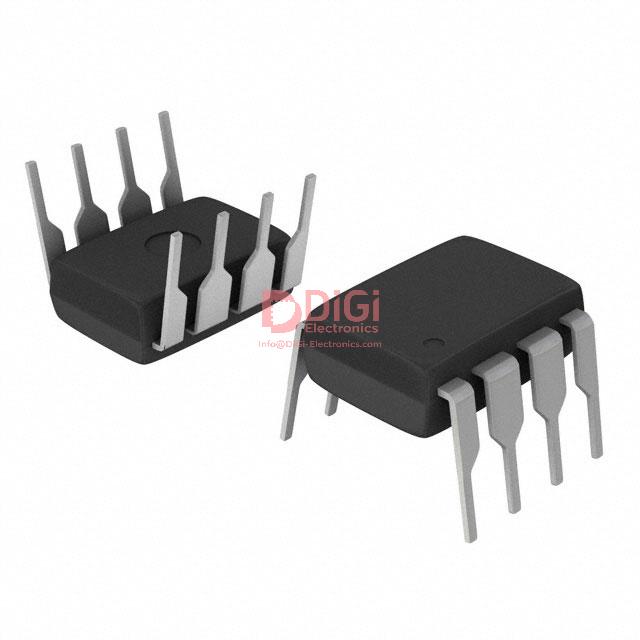
Package, mounting, and compliance details of the VIPER53EDIP-E
The VIPER53EDIP-E integrates seamlessly into mainstream manufacturing flows due to its standard 8-DIP (0.300", 7.62mm) through-hole package. This mechanical format ensures compatibility with automated and manual PCB assembly lines, where through-hole components are preferred for their resilience during soldering, rework, and vibration-prone environments. The DIP package's wide separation between pins facilitates straightforward placement, minimizes the risk of solder bridging, and simplifies optical inspection processes—a critical consideration for high-volume production quality control. The package supports efficient heat dissipation for moderate power levels, accommodating thermal stresses typical in industrial or consumer energy conversion circuits.
Environmental compliance is inherent to the component design, with adherence to RoHS 3 and REACH, making the VIPER53EDIP-E suitable for projects targeting global supply chains and regulatory-sensitive sectors. This ensures downstream users avoid complexities associated with hazardous substance restrictions, streamlining certification and market acceptance. The device maintains a moisture sensitivity level (MSL) of 1, indicating unlimited shelf life under ambient conditions and freeing inventory managers from the constraints of special dry packing or bake-out procedures. This characteristic adds operational flexibility in both production and field maintenance scenarios, reinforcing reliability across the product lifecycle.
For engineers seeking extended thermal capabilities or higher current handling, the VIPER53E portfolio includes the VIPER53ESP-E in the PowerSO-10 surface-mount configuration. This variant enables lower thermal resistance, providing superior junction-to-ambient performance under more rigorous power demands. The enhanced package targets dense layouts and automated surface-mount lines, supporting applications where active cooling, higher component density, or miniaturization drive design choices.
In practical deployment, the choice between DIP and PowerSO packages offers a nuanced balance between assembly method, heat management, and cost control. Experience consistently shows that reliable thermal performance in DIP packages depends not only on pad design but also on copper area allocation and airflow within the enclosure. Furthermore, the low MSL rating simplifies handling protocols, reducing the risk of latent device faults from improper moisture exposure—a factor often underestimated in fast-paced manufacturing environments.
Ultimately, optimizing the adoption of VIPER53EDIP-E or its PowerSO variant relies on a holistic understanding of PCB layout constraints, thermal modeling, and regulatory requirements. Careful integration of these parameters at the early design stage yields both robust electrical performance and streamlined compliance, especially in sectors where reliability and certification drive commercial success. The flexibility provided by diverse package options allows for iterative prototyping and scaling, enabling efficient transition from concept to production with minimal trade-offs.
Potential equivalent/replacement models for the VIPER53EDIP-E
When evaluating potential equivalents or replacements for the VIPER53EDIP-E, the selection process relies on an informed understanding of both the device’s operational mechanics and application-specific demands. At its core, the VIPER53EDIP-E integrates a high-voltage power MOSFET and control circuitry for efficient flyback converter operation, supporting wide input voltage ranges and robust protection functions. Variants such as the VIPER53ESP-E retain comparable core architectures but distinguish themselves through enhanced thermal handling and peak output capabilities, especially in a PowerSO-10 package configuration. This structural distinction enables adaptation to designs where elevated power density or tighter thermal management is pivotal, offering reliable single-range European operation up to 65W.
Functional equivalence extends beyond mere package compatibility; engineers routinely verify parameters such as maximum drain-source voltage, switching frequency tolerance, standby power consumption, and built-in safety mechanisms like overload, overtemperature, and overvoltage protection. When pursuing a drop-in DIP-8 alternative, stringent matching of these electrical characteristics remains mandatory to sustain both regulatory compliance and stable field operation. System-level integration further requires attention to ripple control, EMI mitigation, and transient response, as these factors directly translate to end-product quality.
For broadening the search, examining offerings from STMicroelectronics within the same VIPER series presents a straightforward pathway owing to strong documentation alignment and shared reference designs. In practice, cross-comparison frequently involves alternatives such as ON Semiconductor’s NCP1200/1203 or Infineon’s ICE2QRxx series, known for their competitive integration and switching efficiency. Key differentiators emerge in startup current profiles, burst-mode implementation, and isolation standards, all of which contribute to system design reliability and lifecycle maintenance.
Availability and supply-chain resilience form an integral consideration. Recent project experiences highlight the merit of dual-sourcing strategies, leveraging compatible controllers from different vendors with comparable pinouts and protection features. This tactic reduces risk associated with component lead times, enabling faster prototyping and smoother transitions in large-scale production runs.
A nuanced insight is that optimal replacement selection not only satisfies form and function but also anticipates ecosystem compatibility—such as PCB thermal layout, auxiliary power integration, and manufacturability. Leveraging simulation tools for stress analysis and transient comparison expedites this vetting process, equipping engineers to preemptively identify potential defects or operation margins. Ultimately, focusing on matching the VIPER53EDIP-E’s system-level behaviors—rather than just datasheet specifications—yields a more resilient and scalable solution for complex power conversion applications.
Conclusion
The VIPER53EDIP-E from STMicroelectronics exemplifies a refined integration of control intelligence and power switching capability, specifically tailored for offline flyback converter architectures. At its core, this device merges an advanced pulse-width modulation (PWM) controller with a rugged high-voltage MOSFET, achieving a single-package solution that minimizes both board space and component count. The consolidation of these key functions streamlines layout complexity and simplifies EMI management, a valuable attribute in dense or cost-sensitive SMPS designs.
Architecturally, the VIPER53EDIP-E implements sophisticated primary-side regulation, enabling precise feedback control without reliance on optocouplers. This not only improves total efficiency but also enhances long-term reliability by reducing the number of susceptible passive and optoelectronic components. Embedded in the controller logic are robust fault detection schemes, including overcurrent, overvoltage, and thermal protections. These mechanisms operate autonomously, ensuring rapid system response during transient or abnormal events, which reduces the risk of catastrophic failure and supports adherence to international safety and EMC standards.
Beyond its integral control and protection strategies, the component embodies efficiency-centric features such as burst-mode operation and low standby consumption. These characteristics are critical for meeting stringent regulatory benchmarks like ENERGY STAR or EuP. In practice, the device's dynamic response enables excellent load regulation and easily maintains stable operation across varying AC input ranges, facilitating global power supply compatibility and simplifying the qualification process for geographically distributed products.
Application domains for the VIPER53EDIP-E extend from consumer electronics adapters and auxiliary supplies in industrial automation, to smart appliances and IoT nodes requiring galvanic isolation. Its ability to deliver robust performance under rapid line and load variations positions it as a preferred solution where reliability and compliance are paramount. Selection experience in volume manufacturing contexts highlights a notable reduction in assembly errors and accelerated time-to-market, attributable to both BOM simplification and mature design documentation.
A key differentiator within a competitive market lies in the balance the VIPER53EDIP-E achieves between integration and configurability. While many alternatives demand trade-offs between feature density and ease of implementation, this device offers a harmonious interface: onboard start-up circuits eliminate the requirement for external biasing, while flexible settings for protection thresholds allow adaptation to diverse design envelopes.
Continued exploration of the VIPER53EDIP-E in practical deployment reveals that its operational headroom and EMI performance can materially decrease the iteration cycles typical of SMPS certification. Teams leveraging this part often report higher first-pass yields and measurable improvements in field reliability statistics, suggesting a tangible advantage over more discrete or fragmented approaches. The device not only aligns with current engineering best practices but also anticipates emerging trends, delivering both immediate and enduring value in the evolution of isolated power supply topologies.


