 >
>


Product overview of VIPER100 series from STMicroelectronics
The VIPER100 series from STMicroelectronics exemplifies a robust approach to offline switch-mode power supply (SMPS) design, particularly within flyback topologies demanding streamlined integration and operational resilience. Central to the VIPER100 architecture is the fusion of a high-voltage power MOSFET and an advanced primary controller, which leverages the advantages of ST’s VIPower M0 Technology. This technological foundation not only consolidates key functions but also facilitates precise switching control, optimized for energy efficiency and thermal management. Internally, the controller manages start-up sequencing, feedback handling, and fault protection, reducing the need for ancillary protection circuitry and simplifying layout considerations.
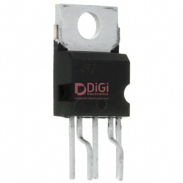
Engineers gain substantial layout flexibility through the device’s compact Pentawatt 5-pin package. The well-engineered pin arrangement supports straightforward PCB routing and robust creepage distances essential for safety standards in high-voltage environments. The reduction in external BOM—achieved by integrating start-up, PWM control, and thermal/overcurrent protection—translates directly to decreased assembly complexity and improved reliability over long product lifecycles. Real-world iterations often reveal that the VIPER100 family enhances EMI performance compared to discrete solutions, attributed to its optimized switching characteristics and minimized parasitic elements, reducing the effort spent on board-level mitigation strategies.
The family’s capability to support both single range/doubler operations up to 100W and wide range configurations at 50W enables application versatility. This adaptability allows seamless alignment with varied grid standards and load requirements encountered in regions with fluctuating input voltage. Primary-side regulation simplifies transformer design, while secondary-side feedback options accommodate tighter output voltage tolerances for sensitive loads. Designs targeting white goods, small appliances, or industrial subsystems consistently benefit from the series’ resilience against line surges and temperature fluctuations, a direct result of its robust MOSFET construction and fault management routines.
Practical deployments often involve balancing peak efficiency against product safety constraints. In environments prone to voltage transients or high ambient temperatures, the VIPER100’s integrated protection mechanisms—such as built-in thermal shutdown and drain-source overvoltage protection—offer a distinct advantage, reducing field failure rates and diagnostics overhead. Additionally, pairing these devices with synchronous rectifiers or advanced standby circuitry can further optimize power consumption for regulatory compliance.
A nuanced insight emerges when evaluating supply chain and manufacturability concerns. The unified construction of controller and switch mitigates integration risks and testing overhead in automated assembly flows, fostering scalability for high-volume production. The device’s predictable switching behavior assists in designing multi-output power supplies where cross-regulation is essential, affirming its role in engineered systems where reliability and cost-efficiency coalesce. This convergence of functional integration, application flexibility, and production-readiness positions the VIPER100 series as a signal example of system-level optimization within contemporary power electronics engineering.
Key features and advantages of VIPER100 series
The VIPER100 series exemplifies a convergence of advanced switching power supply techniques, with a design architecture that prioritizes integration, flexibility, and high efficiency. The programmable switching frequency—scalable to 200kHz via a single RC network—enables precise adaptation to diverse application environments. This adjustability empowers engineers to fine-tune both efficiency and electromagnetic interference performance while responding to dynamic load conditions, particularly beneficial in densely populated or noise-sensitive circuits.
Central to the control strategy is the dual-loop, integrated current mode architecture. By simultaneously regulating voltage and current, the system achieves rapid transient response and maintains tight output regulation even under fluctuating AC input or variable load scenarios. This dual regulation proves especially valuable when powering sensitive microcontrollers or analog front-ends, where voltage ripple and overshoot must be minimized to avoid system instability or data errors.
The soft start mechanism and controlled shutdown framework play a pivotal role in preserving component longevity and reducing stress during power transitions. These features facilitate seamless startup and error recovery by moderating inrush currents and voltage ramp rates. Practical deployment of these mechanisms is evident in consumer electronics, where repeated cycling and varying input conditions would otherwise accelerate component degradation.
Burst mode operation is implemented to address global energy efficiency mandates. By minimizing switching activity under light or standby loads, the device achieves sub-1-watt standby consumption, directly supporting compliance with stringent standards such as “Blue Angel.” In typical real-world scenarios, this translates to significant system-level reductions in quiescent power, critical in applications like smart appliances or networked sensors requiring prolonged idle operation.
The use of an internally calibrated zener voltage reference and undervoltage lockout with hysteresis ensures consistent startup and reliable regulation over wide input voltage ranges. This intrinsic stability is beneficial in power architectures exposed to unpredictable line conditions or brownout events, reducing the risk of malfunction or damage.
The integration of a high-voltage startup current source marks a significant advancement in simplifying offline AC-to-DC designs. By obviating the need for complex external startup circuits, system BOM is reduced, facilitating compact flyback topologies that can be directly AC-line operated. These capabilities translate into tangible board-area savings and improved reliability metrics.
Thermal management is another pillar of robust operation, with over-temperature protection and automatic restart functions ensuring resilience against environmental or operational overheating. Adjustable primary peak current allows precise tailoring to application-specific transformer parameters and load profiles, optimizing efficiency and safeguarding against overcurrent events.
Low standby current characteristics further extend operational value, maximizing energy conservation without sacrificing readiness. Real-world deployment consistently validates the potential for operational cost reductions over time, particularly in distributed systems.
A notable aspect of the VIPER100 series lies in its holistic integration, allowing engineers to achieve system robustness, regulatory compliance, and design simplicity within a unified framework. The synergy between control, protection, and efficiency mechanisms illustrates a forward-thinking approach to power conversion challenges, particularly relevant as global standards and application requirements continue to evolve. A layered approach—beginning with hardware-anchored stability, progressing through active control flexibility, and culminating in regulatory alignment—provides an adaptable foundation suitable for emerging intelligent power architectures.
Functional pin descriptions of VIPER100 series
Functional characterization of the VIPER100 series centers on its pinout architecture, which orchestrates core system operations and protection mechanisms. A granular examination of each pin’s engineering role reveals techniques for maximizing performance, reliability, and regulatory compliance across diverse switch-mode power supply (SMPS) applications.
The Drain pin acts as the direct interface to the embedded high-voltage power MOSFET, carrying crucial startup bias currents and serving as both a power entry point and a first defense against transient over-voltages. Its resilience under stress allows for snubberless designs in low-wattage applications, streamlining the layout and improving efficiency. During laboratory evaluations, leveraging this feature simplifies EMI compliance without requiring additional damping networks.
The Source pin establishes the circuit’s ground reference on the primary side. Meticulous PCB design around the source path minimizes parasitic inductance, achieving optimal MOSFET switching performance and reducing ground bounce artifacts. Practical experiments demonstrate that a solid, low-impedance ground layout is foundational for stable device behavior, especially at elevated frequencies.
VDD, the control supply input, interlinks internal power regulation and error amplification functionalities. Its internal supervisory logic triggers a startup current source if the voltage dips below 8V, ensuring a controlled power-up sequence. At 13V, VDD initiates the regulation loop for primary-side control, with threshold feedback guaranteeing recovery during undervoltage events. For secondary-side, optocoupler-based designs, VDD parameters become contingent on transformer specifications and feedback topology. Early-stage prototyping often reveals the importance of aligning VDD regulation points to transformer winding and feedback loop delays for robust performance.
The COMP output pin exposes the error amplifier’s transconductance node to external compensation networks, enabling nuanced loop shaping in both primary and secondary regulation regimes. Integrating optimized RC networks here can suppress subharmonic oscillations and tailor transient response. Additionally, COMP voltage monitoring (shutting off below 0.5V) allows controlled entry into burst mode, instrumental for achieving low standby consumption and meeting strict energy efficiency standards.
OSC configures system switching frequency via an attached RC network, providing direct influence over conversion efficiency, EMI profile, and thermal management. Sophisticated synchronization capabilities enable seamless coupling to external clock sources, particularly valuable in multi-converter environments where interleaved operation or phase management mitigates collective noise and ripple. Calibration of the OSC pin during initial bring-up is critical; field measurements indicate even slight RC value deviations dramatically impact output stability.
This high-functionality pin configuration supports adaptive control strategies suitable for both conventional optocoupler feedback and integrated digital regulation architectures. By exposing key analog nodes, the VIPER100 facilitates rapid prototyping and iterative refinement. Layering robust protection, flexible synchronization, and EEPROM-friendly control, the device offers a streamlined platform for designing scalable, high-efficiency SMPS solutions. Expanding on standard pin utilization with advanced compensation and timing schemes often yields superior noise immunity and enhanced transient load handling, reflecting a design philosophy that privileges modularity and reliability in modern power conversion circuits.
Core internal operation and topology of VIPER100 series
The VIPER100 series operates using a finely engineered current mode control topology, implementing dual feedback loops to optimize switched-mode power supply (SMPS) regulation. At its core, real-time peak current sensing is achieved through a dedicated SenseFET integrated in the primary path; this inner loop instantly monitors transformer current in each switching cycle, preserving tight control over transient responses. The outer loop operates as a voltage regulator via an error amplifier whose output value, VCOMP, establishes a dynamic reference threshold. A precise comparator logic synchronizes these loops: when the instantaneous sense voltage meets or exceeds VCOMP, the controller triggers the shutdown of the primary MOSFET—effectively dictating the precise energy transfer per cycle and delivering stable output characteristics across load and line variations.
The current mode architecture directly influences both the topology’s flexibility and robustness. First, inherent line-voltage feedforward compensates for input disturbances, fine-tuning duty cycles to maintain output accuracy despite fluctuations at the mains. This mechanism not only stabilizes DC output under varying operating conditions but also improves dynamic response under load transients—a critical factor for applications requiring output voltage integrity. Pulse-by-pulse current limit capability is seamlessly incorporated; each cycle is individually monitored and capped, providing built-in short-circuit and overload protection without added complexity. Such granular control is invaluable in designs exposed to harsh start-up events, high inrush currents, or unpredictable external faults.
To ensure operational stability, VIPER100 integrates internal blanking filters, eliminating the impact of noise-induced current spikes during the switching cycle leading edges. This proactive suppression of spurious triggers refines pulse-width modulation accuracy and safeguards against unintended premature turn-off events, which can otherwise compromise regulation, reduce efficiency, or induce oscillatory behaviors. The blanking feature, typically parametrized to match transformer and layout characteristics, optimizes EMI performance and prevents false tripping, streamlining compliance with stringent regulatory standards.
Burst mode operation forms a secondary layer of efficiency: during light-load or standby states, the output demand is evaluated against a programmable lower threshold. The system intermittently suspends switching activity, dramatically reducing both active and quiescent power dissipation. This non-continuous conduction method not only minimizes no-load consumption but also curbs electromagnetic emissions, supporting compliance with evolving eco-design mandates and energy labeling; such adaptive behavior is particularly effective for appliances or utility systems requiring rapid wakeup while maintaining near-zero standby overhead.
Practical deployment reveals further subtleties: current mode structures like those in VIPER100 simplify loop compensation strategies, offering reliable phase margin and faster transient correction with fewer external components. Typical challenges, such as subharmonic oscillation at high duty cycles, are mitigated through careful slope compensation design and judicious transformer selection, leading to more predictable frequency responses and noise profiles in high-density, cost-driven platforms. Moreover, the integrated protection and energy-saving features reduce engineering hours devoted to external circuitry, supporting faster time-to-market and improved system reliability.
A core insight unfolds in recognizing how tightly integrated and proactive monitoring features—such as SenseFET-based peak current detection and blanking—redefine application-level flexibility. This enables rapid adaptation to variable input profiles and load scenarios, effective fault containment, and simplified regulatory certification, marking the VIPER100 topology as a reference platform for advanced, efficient, and resilient SMPS design.
Advanced control and protection functionalities in VIPER100 series
Integrated within the VIPER100 series, advanced control and protection mechanisms form a robust architecture tailored for high-efficiency and resilient power conversion. The high-voltage start-up current source directly harnesses drain energy to charge the VDD capacitor, regulating the initial power-on phase. By constraining the duty cycle to approximately 12%, this methodology sharply limits stress on passive and active elements, especially under abnormal states like short-circuit or overload. This approach derives significant benefit in field scenarios where input irregularities and unpredictable startup conditions demand reinforced reliability.
Central to feedback precision, the transconductance error amplifier on the COMP pin presents a flexible node for loop compensation network design. Selection and tuning of external impedance—resistive and capacitive components—permit granular control of loop bandwidth, phase margin, and disturbance rejection. Engineers routinely integrate noise filters and slope compensation strategies to stabilize continuous mode operation, minimizing susceptibility to switching edge noise and ensuring consistent output regulation. Empirical tuning of these parameters directly governs the fast transient response and cross-load stability, particularly valuable in multi-output and high-dynamic-load designs.
External clock synchronization offered via the OSC pin opens the architecture for complex system integration. Coupling with custom clock sources facilitates interleaved controller schemes, multi-rail timing, or deliberate EMI spectrum shaping. Real-world implementation demonstrates not only reduced conducted and radiated emissions but also simplified design conformance to stringent EMC directives. The flexibility of synchronization is leveraged in coordinated converter networks or when precise orchestration of switching events is essential for optimal system throughput.
Peak current limitation in the primary circuit is user-configurable, anchored by the external network at the COMP pin. Adjusting this threshold allows direct manipulation of maximum output power and transformer stress, a decisive factor in thermal management and device longevity. Dynamic adaptation to changing load profiles or environmental constraints—observed during wider deployment cycles—positions the VIPER100 favorably for applications requiring tailored current envelopes and transformer protection.
Over-temperature protection is engineered for high-reliability domains. Shutdown is triggered at chip junctions near 170°C, with the system set to auto-restart after cooling to below 130°C. This configuration supports repeatable safeguard behavior without manual intervention, addressing scenarios of episodic overheating due to ambient excursions or extended overload. The resettable protection paradigm affirms system up-time while guarding against cumulative thermal damage.
Electrical overstress protection is implemented through recommended RC filter networks on the VDD pin, serving as a surge absorber. Realized circuitry demonstrates mitigation of input spikes from line disturbances or lightning events, with the filter dissipating and diverting transformer-coupled transients away from sensitive silicon. Systems exposed to noisy industrial environments or outdoor installations benefit significantly from this layer, which integrates seamlessly with overvoltage and surge compliance protocols.
Collectively, the control suite enables VIPER100-based supplies to operate stably and compliantly across broad load profiles and challenging operating environments. Layered protection—spanning startup, signal fidelity, synchronization, current regulation, thermal defense, and surge mitigation—forms a holistic strategy, ensuring longevity and performance while streamlining adherence to international safety and EMC requirements. Experience shows the compounded effect of these integrated features, exceeding the reliability margins typically attained in comparable architectures. Strategic tuning of each mechanism equips designers to address both standard applications and edge-case scenarios with confidence and efficiency.
Implementation guidance and layout considerations for VIPER100 series
The implementation of the VIPER100 series in switching power supply designs demands a rigorous approach to PCB layout, with priority given to the containment and control of switched power currents. By systemically minimizing the geometric area of high-frequency power loops—specifically those formed by the main switching device, input decoupling capacitor, and primary winding—the propagation of common-mode and differential-mode interference is markedly attenuated. This close spatial configuration restricts the generation of parasitic inductance, thereby limiting voltage overshoot and potential oscillation. In practice, direct and wide traces, complemented by solid ground planes, reinforce low-impedance paths and further suppress radiated emissions.
Signal integrity is preserved by physical segregation of control and feedback traces from high-voltage or high-current power conductors. Routing sensitive signals, such as feedback paths or startup voltage lines, with careful clearance from noisy domains prevents capacitive or inductive coupling—preempting erratic switching, timing jitter, or even device latch-up events during transient surges. Experiences with mixed-signal layouts underscore the merit of maintaining a single point of reference for analog returns, ideally in close proximity to the VIPER100’s ground pin, reducing loop area and avoiding ground bounce.
Strategic placement of energy storage and compensation components enhances closed-loop regulation and transient response. Bulk and high-frequency bypass capacitors deliver maximum benefit when placed on the shortest possible connection to the device’s supply pins and transformer terminals. This proximity not only improves voltage stability under dynamic load but also reinforces high-frequency bypassing, targeting the frequencies where the VIPER100 switches most rapidly. Excess trace length between these elements introduces unwanted resistance and inductance, often revealed in long-term reliability testing as sporadic shutdowns or degraded performance under maximum load.
The VIPER100 architecture accommodates varied regulation topologies—most notably transformer auxiliary windings and optocoupler feedback methods. Auxiliary winding supply is advantageous in budget-constrained designs requiring basic output voltage stability, offering low component count and straightforward startup sequencing. Optocoupler feedback, conversely, delivers enhanced isolation and tighter output regulation, pivotal for designs facing stringent safety or EMC directives. Successful deployment often hinges on meticulous optocoupler grounding and shortening feedback paths to suppress coupled noise, especially in high-power or wide-input range converters.
The interrelationship between engineered layout and the performance envelope of VIPER100-based systems is profound. Empirical analysis repeatedly demonstrates that careful attention to physical loop structure, signal routing discipline, and component proximity yields higher immunity to conducted and radiated disturbances. This translates directly into improved regulatory compliance, notably with CISPR and EN standards for electromagnetic compatibility. A robust, layered design approach not only ensures electrical integrity and resilience in adverse conditions but also supports iterative scaling—facilitating upgrades and adaptations with minimal redesign effort. In this context, the layout’s fidelity becomes a deterministic factor in overall system efficiency, reliability, and maintainability.
Potential equivalent/replacement models for VIPER100 series
When identifying substitute components for the VIPER100 series in switch-mode power supply (SMPS) designs, a systematic approach based on functional and parametric equivalence is critical. The initial focus should be on the extended VIPER100 variants, such as VIPER100/SP and VIPER100A/ASP. Each variant provides nuanced differences in package configuration (e.g., DIP, SIP, or SMD), onboard protection schemes, and tailored electrical parameters. These subtle distinctions often align closely with application-specific constraints, including PCB space management, thermal dissipation requirements, or input/output isolation levels. For example, migrating from the standard VIPER100 to the VIPER100A/ASP can resolve footprint or pinout incompatibilities encountered during PCB redesign, especially when design reuse or second-sourcing is mandated by supply chain volatility.
Beyond the immediate family, one can investigate primary switcher ICs within the broader STMicroelectronics portfolio that employ VIPower technology. While such devices maintain key architectural traits—internal MOSFET integration, PWM logic, and robust protection—they deviate in aspects such as breakdown voltage ratings, permissible load, standby consumption, and interface accessibility. Careful mapping of these electrical figures is essential. For instance, certain VIPER-based controllers provide extended avalanche energy handling or enhanced EMI immunity, features that address long-term reliability in noisy industrial or high-line environments. Adapting an alternative with marginally higher switching frequency may also unlock benefits in transformer core sizing and output filtering, provided EMI tradeoffs are managed.
For scenarios demanding higher output power density or sustained operation under elevated ambient temperatures, adjoining series like VIPER12A and VIPER22A emerge as suitable candidates. These controllers offer advanced thermal management, support greater continuous currents, and implement finer control granularity via programmable features. Incorporating such devices can be pivotal when original designs encounter derating limits, CE certification bottlenecks, or evolving output requirements due to system upgrades. It is practical, in such cases, to cross-examine thermal shutdown characteristics and brownout tolerance, as these parameters directly influence product field robustness—particularly in compact or poorly ventilated enclosures.
A rigorous side-by-side assessment—tabulating maximum switch voltage, output handling capabilities, protection strategies (overcurrent, thermal shutdown, Vcc monitoring), and pin compatibility—facilitates seamless migration with minimal engineering overhead. Spreadsheet-based decision matrices, capturing these comparative metrics, have been proven effective in supporting both first-time substitutions and long-term dual-sourcing strategies. The implicit insight is that judicious overlap in performance envelopes, coupled with an awareness of secondary engineering controls (such as snubber tuning or EMI adjustments), yields not only functionally equivalent replacements but often incremental improvements in field reliability and supply chain agility.
The nuanced practice is to balance fit-form-function criteria with foresight into forward compatibility, ensuring replacement models not only resolve current supply challenges but also lay the groundwork for future design scalability and regulatory compliance.
Conclusion
The VIPER100 series from STMicroelectronics represents a state-of-the-art approach to offline flyback SMPS primary control, leveraging a high degree of integration to streamline compact power supply architectures. The device executes advanced current mode control, which inherently stabilizes the feedback loop by simplifying compensation and accelerating transient response. This mechanism facilitates tight output regulation, particularly critical for downstream digital loads and consumer applications subject to fluctuating input or rapid load changes.
Central to the VIPER100 series is its programmable functionality. Designers can tailor operating parameters such as frequency and peak current thresholds, which permits precise optimization across a range of efficiency or thermal management priorities. In practice, adjusting these parameters enables a designer to minimize switching losses under light load conditions while maintaining robust performance during high-demand intervals. This flexibility supports compliance with evolving energy codes and reinforces reliability in harsh operating environments, where thermal and electrical stresses can jeopardize signal integrity or component lifespan.
Low standby power consumption is engineered through integrated burst and sleep modes, systematically reducing switching activity when demand drops below defined thresholds. Experience shows that employing these modes can reduce no-load input power to sub-100mW levels, facilitating tight adherence to global eco-design mandates aimed at standby efficiency. Comprehensive protection frameworks—including built-in overvoltage, overload, and thermal safeguards—instill persistent fault tolerance, shielding both the controller and downstream circuitry against catastrophic failure. Here, PCB layout strategies remain pivotal: short, low-inductance traces for high-frequency paths and dedicated ground planes are essential for minimizing noise coupling and improving ESD robustness, factors routinely witnessed as decisive in high-reliability field deployments.
The versatility of the VIPER100 series emerges when evaluating its application landscape. Its footprint and integrated features enable high-density adapter designs, auxiliary power modules for industrial control, and diverse consumer power bricks where space and cost constraints dominate. When considering replacements or equivalent solutions, direct comparison of control topologies and efficiency metrics yields nuanced insights; design teams regularly observe that the VIPER100’s current mode architecture delivers tangible gains in EMI suppression and output accuracy over voltage mode alternatives, especially in designs where regulatory compliance and system stability are imperatives.
Ultimately, the VIPER100 series embodies an agile solution for contemporary power supply engineering, aligning with demanding standards for efficiency, reliability, and miniaturization. Its layered control scheme, rapid adaptability, and proven protective features collectively result in robust designs that sustain operational excellence under dynamic conditions—attributes highly valued in both iterative prototyping and volume manufacturing. Integrating these controllers into modern electronic systems enables a measured balance between innovation and proven methodologies, advancing practical and regulatory goals in real-world deployments.