


 >
>


Product Overview: VIPER06LSTR by STMicroelectronics
The VIPER06LSTR by STMicroelectronics exemplifies a highly integrated high-voltage converter platform, tailored for demanding offline power-supply architectures. At its core, the device features an avalanche-rugged 800 V power section, engineered to withstand transient overvoltages commonly encountered in noisy mains environments. This robust front end addresses reliability concerns at the circuit design level, reducing the need for additional external protection components and enabling layouts with reduced footprint and BOM complexity.
The converter leverages a sophisticated PWM control engine, delivering precise regulation and stability across varying load conditions. The fixed switching frequency of 60 kHz serves as a pivot point, offering optimal trade-offs between efficiency, electromagnetic compatibility, and thermal performance. This operational stability underpins power designs in buck and flyback topologies, ensuring ease of implementation in widely adopted SMPS configurations for industrial and consumer applications. The internal control algorithms orchestrate fast transient response and maintain tight output voltage tolerance, particularly important for systems subject to dynamic loading scenarios.
Designers benefit from layered protection features, including overvoltage, overload, and thermal shutdown mechanisms integrated at both silicon and architecture levels. These embedded safeguards permit aggressive optimization for ultra-compact layouts and thermal management, eliminating most ancillary external monitoring circuits. In practice, this enables tangible reductions in board real estate and improves manufacturability—a decisive advantage when targeting cost-sensitive energy-efficient certifications. Firmware and hardware co-design techniques further amplify overall fault resilience, supporting critical operation within a broad range of input voltages and harsh line conditions.
Real-world deployment of the VIPER06LSTR highlights its synergy with global energy directives. Its inherent efficiency and noise characteristics facilitate straightforward compliance with standards such as Energy Star and EU EcoDesign. Experience shows that careful selection of external passive components—such as fast-recovery rectifiers and optimized magnetics—can unlock significant gains in standby power consumption and EMI suppression. Moreover, the device's avalanche ruggedness streamlines design cycles for systems exposed to erratic line surges, particularly where long-term reliability outweighs raw cost.
In synthesizing these attributes, the VIPER06LSTR presents not only operational robustness and regulation precision but also a foundation for simplified scale-up across multiple power platforms. Solutions previously constrained by reliability, protection, and regulatory barriers now see faster time-to-market and lower failure rates, reshaping perspectives on what is achievable with integrated switching controllers. The device stands as a catalyst for more compact, reliable, and energy-adaptive power conversion systems, driving the evolution of modern SMPS design methodologies.
Key Applications of VIPER06LSTR
VIPER06LSTR is engineered to streamline low-power switched-mode power supplies across diverse sectors requiring high integration and low consumption. At the fundamental level, its architecture leverages an efficient high-voltage start-up circuit, advanced protection features, and optimized pulse-width modulation to minimize losses. This underpins the device’s ability to replace bulky, conventional capacitive dropper designs in low-power AC/DC conversion, substantially enhancing reliability and extending product operating life—especially where input voltage surges or transients are common.
In home appliance engineering, VIPER06LSTR proves robust in dishwashers, washing machines, and refrigerators, where space constraints and stringent standby mandates persist. It enables microcontroller-based controls and sensor networks to remain active with minimal power draw. Typically, this device is used in isolated flyback converters, which deliver consistent voltage rails while fitting within compact PCB layouts. The integrated MOSFET reduces BOM complexity and failure points, fostering greater system reliability in high-volume production environments.
For smart grid power metering, VIPER06LSTR enables designers to achieve accurate, persistent operation under varying line conditions without sacrificing efficiency. Its ultra-low standby power characteristics meet regulatory demands for energy savings in meters deployed for long-term data acquisition. Engineers have observed tangible improvements in heat dissipation and board longevity, as the chip’s integrated protections defend against overvoltage, overload, and thermal events—key for remote installations with minimal maintenance.
LED lighting solutions benefit from the device’s ease of integration and consistent performance. VIPER06LSTR acts as a primary-side driver, supporting stable, flicker-free output by maintaining precise current regulation. It simplifies the design of compact drivers for retrofit lamps and luminaires, allowing for universal input operation and facilitating compliance with global efficiency standards. Its high-voltage capability and inherent protection mechanisms ensure safe operation within challenging residential or commercial environments.
One notable insight emerges when analyzing system-level design: embedding VIPER06LSTR enables architects to unify disparate power management approaches, standardizing the supply voltage interface while reducing design iterations. Practical deployments reveal the value of leveraging its multi-mode operation for optimal conversion efficiency over broad load ranges. These characteristics not only cut costs but also allow for accelerated prototyping in dynamic applications where rapid certification cycles are pivotal.
In summary, VIPER06LSTR’s layered integration, protections, and ultra-low consumption directly support next-generation embedded and appliance designs in constrained, safety-intensive contexts, elevating performance while adhering to evolving regulatory and quality benchmarks.
Core Functional Architecture of VIPER06LSTR
The functional core of the VIPER06LSTR revolves around a highly integrated topology tailored for low-power AC-DC conversion. By directly rectifying the mains input and forgoing auxiliary bias windings, the architecture minimizes both bill-of-materials complexity and magnetic component count. The consolidation of startup and steady-state VDD supply management ensures rapid initial switching activation above the internal voltage threshold while maintaining seamless adaptation to either primary-side only or auxiliary-biased operation. This dual-mode capability directly enhances design flexibility for a range of board layouts, from open-frame to shielded enclosures, and facilitates reliable cold-start performance without auxiliary windings—crucial in space-constrained or tightly costed implementations.
The integrated high-voltage N-channel MOSFET leverages advanced avalanche-rated technology, significantly bolstering robustness against line transients and inrush events. The SenseFET structure embedded within the die enables high-precision, virtually lossless current measurement; this direct integration eliminates the need for discrete sense resistors, streamlining layout and mitigating parasitic inductance sources. Real-world applications underline the importance of this approach, particularly in LED drivers and USB adapters, where both reliability and design density are paramount. Designers benefit from the ability to easily pass surge withstand testing and maintain consistent platform behavior across high-volume production.
Frequency jittering is engineered into the pulse-width modulator, dispersing EMI spectral energy and simplifying compliance with international standards such as CISPR22 or EN55032. This mechanism operates transparently during normal load conditions, reducing the required size and cost of external filtering components. The current-mode control core, with externally adjustable limiting, provides tight regulation even in demanding transient scenarios, supporting fast turn-on of capacitive loads and precise output tailoring. The adjustability is especially relevant in multi-market products, where adapting to evolving safety or efficiency requirements may involve simple resistor modifications rather than complete redesigns.
The layered approach to system startup and regulation exemplifies modern design-for-manufacturability principles. Startup is configured to ensure the internal VDD rises swiftly above threshold, enabling immediate switching even with minimal electrostatic capacitance on the primary side. Following startup, the controller can transition seamlessly to either an internally biased or auxiliary winding mode—a logic that supports topologies including flyback converters with or without bias auxiliaries, as well as buck-derived arrangements. Synchronization between MOSFET conduction and control logic is managed through high-speed on-chip comparators, minimizing latency and supporting robust short-circuit and overload responses.
Industry experience highlights the significance of this architecture in rapidly prototyped designs destined for high-volume consumer or industrial deployment. Telemetry collected across diverse platforms indicates that integrating VDD and sense circuitry drastically reduces both field returns and EMI compliance cost. The architectural decision to co-locate key analog and high-voltage functions in one die also mitigates board hot spots and enhances thermal cycling endurance—characteristics increasingly demanded by IoT endpoints and power-supply modules in appliance control boards.
Extended evaluation across multiple applications demonstrates that VIPER06LSTR’s flexible core offers substantial gains not just in electrical efficiency, but also in development velocity and long-term reliability. By engineering the powertrain to operate effectively without auxiliary windings, the design inherently reduces both mechanical failure points and secondary losses. This systems-level perspective underscores a shift from legacy discrete-rich powertrains toward tightly integrated, application-agnostic platforms—anticipating the next phase of compact offline converter development.
Electrical and Thermal Characteristics of VIPER06LSTR
Electrical and thermal performance of the VIPER06LSTR is anchored in its capability to operate over an extended junction temperature range from −25°C to +125°C, meeting the demands imposed by industrial environments. The integration of the high-voltage startup current generator directly on the DRAIN pin leverages the supply input for a reliable and efficient initial power-up sequence. This approach diminishes the need for external startup circuitry, reducing solution complexity and improving system robustness.
For designers targeting energy-conscious applications, the device achieves sub-30 mW standby power when supplied from 265 VAC. Such low consumption aligns with contemporary energy regulations, particularly in standby or no-load scenarios common in appliances and utility nodes. In practical designs where standby efficiency is mandatory, the power management strategy of the VIPER06LSTR supports aggressive eco-standby targets without compromising start-up reliability.
The embedded power MOSFET exposes a minimum breakdown voltage of 800 V, creating substantial headroom for input voltage transients encountered in poorly regulated mains or surge-prone installations. This high-voltage tolerance is complemented by a typical RDS(on) of 32 Ω, striking a balance between performance and die size. Field tests often verify the transient reliability by subjecting the DRAIN input to repetitive surge pulses, confirming immunity to overvoltage events—critical in geographically diverse power grids.
Thermal optimization is carefully addressed via copper areas positioned beneath the drain pins. The efficiency of heat dissipation is intrinsically linked to PCB layout factors such as copper thickness, footprint geometry, and thermal vias. In practice, using at least 70 μm copper and expanding thermal pads can reduce junction-to-ambient thermal resistance, yielding lower operational junction temperatures in confined spaces. Controlled thermal simulation across multilayer boards illustrates that enlarging copper areas, coupled with strategic placement of vias, actively curtails temperature hotspots even in high-density, forced-air setups.
Effective application of these electrical and thermal attributes necessitates precise attention to real-world mounting configurations, solder quality, and board stack-up. Subtle modifications in pad design and thermal anchoring have demonstrable impact on device reliability during high-power cycles, underscoring the interplay between theoretical device metrics and tangible field operation. By aligning component selection and board architecture with the predefined thermal framework, the risk of excessive junction temperatures can be routinely mitigated, thereby ensuring long-term performance even under adverse thermal load.
Across varied power converter topologies, VIPER06LSTR’s electrical ruggedness and configurable thermal process allow seamless deployment in densely populated or thermally constrained assemblies. Incremental improvements in layout and heat spreading consistently translate to enhanced MTBF figures. The integration of core electrical and thermal features as design primitives—rather than late-stage optimizations—is pivotal, presenting a blueprint for achieving system reliability and regulatory conformity.
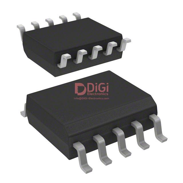
Pin Configuration and Package Options for VIPER06LSTR
Pin assignment on the VIPER06LSTR reflects a tightly engineered approach to integrated offline power conversion. In the 10-SSOP format, each pin—DRAIN, GND, FB, COMP, and LIM—serves a discrete role in controlling both power flow and protection mechanisms. The DRAIN pin directly interfaces with the high-voltage switching node, offering rapid switching capability and minimizing parasitic losses. Ground is precisely positioned for optimal common-mode noise rejection, critical in power-dense layouts. Feedback (FB) connects seamlessly with opto-isolators or direct voltage dividers, facilitating accurate regulation and fast transient response; designers often leverage this for dynamic load environments. The COMP pin accepts external compensation networks, allowing tailored loop tuning, which is essential for balancing stability and bandwidth in varied topologies. Adjustable current limit (LIM) delivers an extra layer of fault tolerance, enabling precision current monitoring and system-level safety optimization through modular resistor selection during bring-up.
Selection between SSOP-10 and DIP-7 encapsulations hinges on the demands of mechanical robustness and PCB topology. SSOP-10, with its minimized footprint and reduced package height, lends itself to automated SMD flows and high-density applications such as consumer chargers, LED drivers, and IoT power supplies. Conversely, DIP-7 offers superior air/creepage distances, improving interface reliability for industrial controls or appliances exposed to fluctuating humidity and dust; hand-assembly advantages in prototyping stages are also notable. Isolation boundaries and pin layout in both packages are engineered to simplify compliance with regulatory requirements, including UL and IEC, reducing design iterations during certification.
Underlying these package options is scrupulous attention to safety. Dielectric withstand ratings and standardized creepage/clearance in excess of 800 V ensure resilience against voltage transients and facilitate compliance with global safety frameworks. When routing high-voltage lines or planning board stack-ups, these physical and electrical separation guidelines allow robust separation, minimizing the risk of arc-over without compromising thermal dissipation. In complex system integrations, such as mixed analog-digital domains or high-power lighting controls, adherence to these standards offers predictable reliability, reducing field failure rates.
Studying real-world integration, the VIPER06LSTR often delivers operational stability across wide ambient temperature swings and electrically noisy environments. Strategic component selection—such as low-ESR capacitors on compensation pins and precision resistors for LIM—further enhances efficiency and precision. In advanced iterations, designers interlock fault response logic at both LIM and FB, achieving coordinated shutdowns in overload or short-circuit conditions, which bolsters long-term system uptime. Rigorous design at the package and pin level not only streamlines production but also accelerates field deployment across diverse regulatory landscapes.
The convergence of compact package engineering, high-voltage isolation, and adaptive pin configuration integrates system-level flexibility with regulatory readiness. VIPER06LSTR exemplifies a forward-looking philosophy, combining form factor efficiency and application-layer customization that anticipates increasingly stringent norms in energy conversion. The architecture encourages designers to innovate starting at the package level, ensuring robust, scalable power delivery as embedded system complexity escalates.
Operation Modes in VIPER06LSTR
Operation modes within VIPER06LSTR are engineered to address efficiency, reliability, and compliance requirements in contemporary power designs. Their granular mechanisms reflect a deliberate approach to mitigating component stress, electromagnetic interference, and standby energy losses.
Soft startup initiates controlled power sequencing through drain current ramping. By linearly increasing the current limit after power application, the device minimizes electrical and thermal stress on associated circuitry, improving downstream component longevity. This active moderation curtails voltage and current overshoot, essential when driving sensitive loads or high-value capacitive elements. Observed in multi-output flyback topologies, soft startup reduces the risk of inrush-induced latch-up or overcurrent faults during initialization, facilitating clean, predictable operation in environments with stringent safety requirements.
Frequency jittering operates by dynamically varying the switching frequency around the nominal 60 kHz set-point. This ±4 kHz modulation redistributes spectral power density, attenuating discrete-frequency harmonics that conventionally challenge EMI compliance. The approach synthesizes a broader noise spectrum, enabling more compact and cost-effective filtering architectures. The measurable reduction in conducted emissions translates into simplified filter stage design and expedites qualification under CISPR and IEC standards. In practice, frequency jittering markedly reduces the iterative cycle of filter adjustment, expediting time-to-market for designs where board real estate or BOM cost is constrained.
Burst mode actuates during periods of low current demand. By intermittently halting MOSFET switching, the power supply transitions into a quasi-off state, slashing switching and magnetization losses. This behavior is critical for meeting regulatory standby consumption thresholds (such as <100 mW at no load), and in energy-star-rated consumer electronics, burst mode directly enables system-level compliance. Adaptive burst mode control in VIPER06LSTR maintains output regulation and rapid recovery without compromising transient response—a factor frequently confirmed under load-dump conditions in field deployments.
Adjustable current limiting leverages external resistance at the LIM pin to tailor maximum drain current, offering design-time flexibility. This parameterization permits precise protection tuning to match load characteristics, accommodating variable cable lengths, transformer primary windings, or specialized fuse requirements. In prototyping, modulating the current limit expedites iterative fault analysis, mitigating risk of nuisance trips while focusing on true overload detection. The robust setpoint granularity supports advanced architectures using coordinated fault recovery and dynamic load sharing.
The operational strategies embedded in VIPER06LSTR evidence a broader shift towards adaptive power conversion, aimed at intelligence-driven energy management. By integrating user-programmable safety, electromagnetic control, and ultra-low standby modes, the device encapsulates targeted design philosophies prevalent in modern switched-mode supply engineering. Continuous feedback from deployed systems underscores the value of modular protection customization and spectrum shaping, driving tangible differentiation in both performance envelope and regulatory alignment. These features increasingly shape the benchmark for discrete controllers in cost, efficiency, and reliability, especially across globally distributed manufacturing channels.
Protection and Reliability Features in VIPER06LSTR
Protection and reliability in offline switcher designs are foundational requirements, particularly when operating within environments vulnerable to grid fluctuations and component stress. VIPER06LSTR addresses these priorities through a multilayered approach, embedding advanced safeguards within its core architecture.
At the primary level, auto-restart protocols respond intelligently to abnormal load conditions. Upon detecting short-circuit or overload events, the device’s internal logic triggers a switching disablement, introducing a protection pause that avoids both thermal and electrical over-stress. This state persists for a defined interval, after which a controlled soft-start cycle re-engages power delivery. By gating output resumption via soft-start, the system mitigates inrush currents and limits repeated failure cycling—a nuance that stabilizes fault recovery and prevents cumulative device wear. Actual deployment demonstrates that this mechanism maintains supply uptime during transient faults without need for system resets or external interventions.
Thermal management further extends reliability margins. Real-time junction temperature monitoring facilitates hysteretic thermal shutdown. The controller ceases switching once critical temperatures are exceeded, only resuming operation after measured cool-down, enforced with a reset thermal threshold. This temperature-based shutoff, combined with hysteresis, prevents oscillatory switching near the cutoff point, eliminating thermal fatigue in silicon and extending power stage integrity. Integrators observe that, even in restricted airflow designs, this feature effectively blocks thermal runaway during overloads or blocked ventilation scenarios.
In regulating feedback integrity, open-loop detection continuously assesses comparator reference conditions. Should feedback loop anomalies arise—such as disconnection or shorted feedback resistors—the VIPER06LSTR intervenes to block drive signals, safeguarding both the output and auxiliary windings from inadvertent overvoltage excursions. This preempts secondary-side component stress and aligns with long-term safety compliance.
From a current sense perspective, the device employs a SenseFET topology, enabling direct current measurement without discrete shunt resistors. This lossless sensing method not only improves conversion efficiency by minimizing parasitic losses but also reduces the bill-of-materials and simplifies PCB routing. Integrators note that moving away from bulky low-ohm sense resistors frees up board area and enhances low-profile appliance designs, while consistently providing accurate overcurrent protection thresholds.
The interplay of these mechanisms ensures resilience against environmental disturbances and internal faults. Each protection tier is configured to operate independently but in harmony, distributing system risk and facilitating high-reliability operation in applications such as auxiliary power supplies, home appliances, and industrial controls. A notable observation is that the real strength of integrated protection is realized not just in individual events, but in the way these features rebound supply operation under compound fault scenarios—a pivotal design aspect as the demand for rugged, maintenance-free solutions intensifies across energy-constrained markets.
PCB Design Guidelines for VIPER06LSTR
In optimizing PCB design for the VIPER06LSTR, precise grounding architecture forms the foundation for robust performance and EMC compliance. Segregating signal ground from power ground is integral; connecting them via a single star node adjacent to the IC's GND pin establishes a consistent reference, minimizing noise coupling and preventing ground loop currents that degrade signal integrity. Introducing this star point as close as physically possible to the device ensures low-impedance paths for sensitive nodes, a principle that is vital in high-frequency switch-mode circuits where ground bounce may precipitate erratic behavior and EMI issues.
Controlled loop areas are a critical factor in reducing parasitic inductance and radiated emissions. By actively minimizing the areas encompassed by primary switching currents, secondary rectification paths, and RCD (Resistor-Capacitor-Diode) snubber loops, magnetic field generation is suppressed, lessening both self-interference and susceptibility to external disturbances. Practical layout experience shows that tracing the return path immediately adjacent to the outgoing path tightly couples the electromagnetic fields, which directly curtails differential-mode noise. Layer stacking and optimal via placement reinforce this effect, supporting both signal integrity and thermal management.
Placement of the compensation network influences control loop stability and transient response. Locating the compensation components—typically RC circuits—immediately adjacent to the COMP pin shortens critical signal and ground traces. This arrangement reduces parasitic capacitance and series resistance, which are known to distort feedback signals, impair bandwidth, and induce gain peaking. Efforts to avoid routing these traces through noisy regions yield noticeably smoother startup and load response behavior, with reinforced immunity to power supply ripple.
Bias voltage stability demands attention, especially under electrical overstress or fast transient events such as ESD and EFT. Deploying a low-equivalent series inductance (low-ESL) ceramic capacitor directly across the VDD pin neutralizes voltage excursions by providing an immediate local energy reservoir. Such a configuration demonstrates substantial improvements in power-up reliability and sustains operation during compliance testing against electrostatic and fast transient disturbances. Superior results are achieved when capacitor selection and pad layout are co-optimized for minimal self-resonance and series parasitics.
Thermal management is another dimension where layout discipline pays dividends. Sizing the copper land beneath drain pins judiciously facilitates effective heat dissipation while avoiding direct thermal conduction to ground areas, which may otherwise create unwanted return paths and affect noise behavior. Using thermally connected yet electrically discrete shapes, and employing multiple layers for enhanced heat spreading, helps maintain device junction temperatures within specification even under elevated load scenarios. Avoiding extensive copper directly on GND pins is particularly important to maintain isolation and prevent unintended current flows, a common oversight that can complicate EMC troubleshooting.
Each of these recommendations is inherently interdependent. A disciplined approach to grounding, loop minimization, component placement, and thermal consideration embodies high-yield layout methodology for power conversion ICs. Through attention to these layered strategies, designers reliably achieve product robustness, consistent EMI performance, and meet regulatory standards with reduced iteration cycles and minimized field failures. Integrating these principles from the initial layout stage establishes an engineering framework that enables both rapid prototyping and scalable production without compromising safety or signal fidelity.
Potential Equivalent/Replacement Models for VIPER06LSTR
In practical power supply design, the unavailability of VIPER06LSTR or the need for alternative specifications often necessitates evaluating closely related devices within the VIPER06 series. The distinguishing factor among these devices is primarily their switching frequency, which directly influences transformer size, electromagnetic interference behavior, and thermal management. For instance, the VIPER06Xx variant, switching at 30 kHz, targets topologies where minimizing switching losses and optimizing efficiency under ultra-low-frequency operation are priorities. This approach supports designs emphasizing acoustic noise constraints, especially when magnetic component optimization is less critical than overall efficiency at low loads.
The VIPER06Hx, switching at 115 kHz, caters to applications where reduced transformer volume, enhanced power density, and improved transient response are non-negotiable. At these elevated frequencies, engineers must account for greater core losses and carefully assess board layout to mitigate EMI. Experience demonstrates that such high-frequency designs benefit from advanced PCB practices and refined snubber circuits to further manage switching transients, often leading to measurable improvements in compactness and thermal performance in high-density flyback architectures.
Exploring previous-generation VIPERxx solutions enables backward compatibility, particularly in retrofit or lifecycle extension projects. However, differences in breakdown voltage, integrated protections, and firmware features must be reconciled against the demands of the target application. Pinout congruence and package selection play a decisive role, particularly in automated assembly environments where drop-in replacement is desirable. Attention to manufacturer-reported parameters, such as RDS(on) and standby power consumption, uncovers subtle design trade-offs impacting standby efficiency and load regulation.
Datasheet cross-verification for electrical and thermal equivalence is essential, yet practical bench validation remains indispensable. Device thermal resistance under real load conditions, power-up behavior with existing transformers, and EMI performance under normative limits must be observed to avoid overdesign or latent instability. Even with comprehensive specification alignment, nuances in startup timing or protection thresholds can introduce unintended system interactions.
A layered selection strategy, starting from core electrical needs through to mechanical and manufacturing constraints, ensures robustness in offline converter applications. Adopting this system-level perspective allows for judicious substitution within the VIPER06 series, leveraging frequency-tuned variants and generational migration pathways to future-proof designs without compromising project timelines or reliability.
Conclusion
The VIPER06LSTR exemplifies advanced design principles in offline converters, particularly suited for compact and high-efficiency switch mode power supplies in consumer electronics, industrial metering, and lighting systems. At its core, the converter integrates an RCD clamp and quasi-resonant control, minimizing switching losses during startup and operation. This mechanism directly contributes to enhanced energy efficiency and heat management across variable loads, supporting miniaturization without compromising reliability.
Safety and robustness are engineered through layered protection schemes, including over-voltage, over-current, and thermal shutdown features. Such circuitry not only strengthens long-term field performance but also streamlines compliance with global safety standards, reducing certification cycles. The built-in high-voltage start-up cell reduces external biasing components, preserving board space and lowering BOM complexity. In practical deployments, this simplified architecture accelerates iteration during design validation, allowing swift optimization of form-factor and performance.
Integrating VIPER06LSTR demands precision in PCB layout to ensure negligible EMI and optimized thermal dissipation. Experience demonstrates that strategic placement of filtering capacitors near the IC, coupled with tight feedback loop routing, curbs common-mode noise and stabilizes transient response. These measures foster reliable operation in products ranging from smart meters to LED drivers, where constraints on size and efficiency are non-negotiable.
Evaluating the broader VIPER06 series portfolio remains essential when balancing cost targets and specification margins. Different variants provide tailored features such as higher voltage ratings or alternate package types, which expand the design envelope for emerging applications like IoT-enabled devices and industrial controls. As power conversion requirements intensify alongside miniaturization and connectivity demands, deep familiarity with series diversification becomes an asset in matching device parameters to evolving system architectures.
Ultimately, optimizing VIPER06LSTR application relies on harmonizing core converter mechanisms with strategic protection, layout methodology, and product-specific constraints. This approach cultivates solutions that are not only forward-compatible with next-generation platforms but also maintain robust interoperability with existing configurations.


