


 >
>


Product Overview of VIPER100ASP-E by STMicroelectronics
The VIPER100ASP-E, designed by STMicroelectronics, exemplifies a modern approach to offline Flyback power supply design. Its core innovation lies in the monolithic integration of a high-speed PWM controller and a 700V/3A vertical power MOSFET, enabled by VIPower M0 Technology. This configuration consolidates the control and switching elements onto a single die, minimizing parasitics and enhancing switching efficiency. Consequentially, designers gain a platform with markedly improved energy conversion rates, particularly beneficial for applications requiring stringent power regulation and thermal management.
Internally, the PWM controller employs robust feedback mechanisms, leveraging precise duty cycle modulation to accommodate dynamic load profiles and input voltage variations. This adaptability serves both universal input designs, supporting up to 50W output, and higher-power scenarios—extending to 100W in dedicated single-range or doubler configurations. The vertical MOSFET structure further delivers low RDS(on) and rapid switching characteristics, promoting reduced conduction losses and improved electromagnetic compatibility. By tightly coupling these elements, the device addresses critical performance targets in modern AC-DC converters used within industrial automation, appliance control, and auxiliary power modules.
From a system engineering viewpoint, the VIPER100ASP-E offers significant reductions in external component requirements compared to conventional discrete solutions. The integrated platform eliminates multiple passive and active components, which simplifies PCB layout and shortens development cycles. Fewer parts translate into lower failure rates, directly influencing long-term reliability, especially in environments exposed to wide temperature swings or line transients. Additionally, the device includes essential safety and protection features—such as overvoltage, overload, and thermal shutdown—embedded at the silicon level, alleviating the need for supplementary circuit blocks and enhancing compliance with international safety standards.
Practical implementation highlights include streamlined EMI compliance, enabled by coordinated switching control and optimized turn-off dynamics inherent to the MOSFET-controller integration. In typical design cycles, leveraging the device in Flyback topologies—especially with universal inputs—results in consistent performance even under fluctuating supply conditions. Implementation nuances, such as careful heat-sinking and proper snubber selection, further maximize operational efficiency and longevity. For high-reliability sectors, the integrated solution provides a stable foundation for scalable power architectures, facilitating rapid prototyping and iterative refinement.
Distinctively, the VIPER100ASP-E bridges the gap between high-voltage MOSFET performance and configurable control logic. This synergy points to broader trends in integrated power semiconductors, where performance, safety, and simplicity must coalesce to meet the evolving demands of compact and efficient power conversion. The device not only meets immediate energy efficiency goals but also embodies the design philosophy of reducing complexity without compromising robustness—an approach that aligns closely with contemporary system integration standards and forward-looking engineering practices.
Key Features and Functional Architecture of VIPER100ASP-E
At the heart of the VIPER100ASP-E lies a meticulously engineered control system designed to deliver high efficiency, reliability, and adaptability across a wide range of offline switch-mode power supply (SMPS) applications. The device’s architecture leverages a highly adjustable switching frequency, extending to 200kHz, which permits precise alignment of converter performance with system-level efficiency targets and EMI (Electromagnetic Interference) constraints. By fine-tuning this parameter, designs can achieve the optimum balance between transformer size, thermal dissipation, and electromagnetic noise, lessons often surfaced during late-stage qualification testing where unforeseen EMI hotspots may occur.
Central to its regulation strategy is the implementation of a stable current-mode control scheme. This approach ensures predictable dynamic response under fast-load transients, as well as robust line and load regulation. Integrating this topology enables straightforward compensation design, particularly when targeting compact, cost-sensitive power supplies where board real estate and BOM (Bill of Materials) cost are pivotal constraints. The current-mode structure also facilitates inherent cycle-by-cycle current limiting, forming a core component of the device’s multi-tier protection system.
The soft-start function, tightly integrated within the controller, initiates power-up sequences with controlled inrush currents, minimizing voltage overshoot and mechanical stress on downstream components. This sequenced startup, combined with the controlled shutdown capability, fosters graceful recovery from fault conditions, an essential factor in safety-critical or high-availability platforms. In practical design implementations, these features translate to increased power converter lifespans and reduced maintenance intervals—outcomes often only appreciated after extended field operation.
Automatic burst mode operation is activated under low-load or standby conditions, significantly curbing energy draw and facilitating compliance with aggressive energy efficiency standards such as the "Blue Angel" eco-label. The scheme’s ability to reduce system consumption below 1W stands as a best-in-class achievement for no-load and light-load operation, crucial for consumer and industrial products subject to regulatory audits. The internal logic seamlessly transitions between normal and burst modes, stabilizing auxiliary supply rails without user intervention.
Over-temperature protection integrates precision thermal sense circuitry with fast shutdown logic, ensuring the device remains within safe operating limits under elevated ambient or overload scenarios. A hysteretic undervoltage lock-out guards against erratic power cycling during brownout events, a common pain point identified in geographically diverse deployment locations. This dual-layer resilience framework diminishes the risk of latent failures and operational interruptions.
Reliability is further bolstered by an internally trimmed Zener reference voltage and on-chip startup supply circuitry. These block-level integrations reduce the external component count, simplify PCB layout, and mitigate variance from discrete reference errors or startup failures. In fielded systems, this translates to tighter output regulation and shorter mean-time-to-repair.
Peak current limitation is made user-configurable, supporting a broad range of transformer and output topologies without sacrificing overcurrent robustness. At the same time, exceedingly low standby current enables design teams to meet strict system-level energy budgets even when the power stage is idling. This dual focus streamlines platform reuse across diverse end products, from home appliances to industrial sensor nodes.
Architected for design flexibility, VIPER100ASP-E supports both primary-side and secondary-side feedback regulation while minimizing the need for external circuitry. This adaptability accelerates design cycles and improves manufacturing yield, particularly in isolated power modules. The interoperability with various feedback techniques unlocks rapid prototyping and smooth design iteration paths, an advantage consistently observed in fast-paced development programs.
A consistent thread across the device’s features is the unification of analog performance, fault tolerance, and regulatory compliance, creating a foundation for power supplies that endure both engineering scrutiny and real-world deployment. By integrating core insights from demanding application domains, the VIPER100ASP-E illustrates a system-level understanding of modern power design challenges—where robustness, efficiency, and ease of deployment are not optional, but essential characteristics.
Electrical and Thermal Specifications of VIPER100ASP-E
Electrical and thermal specifications are pivotal factors in evaluating the robustness and suitability of the VIPER100ASP-E for high-voltage power conversion systems. At its core, the device integrates a high-voltage MOSFET capable of withstanding drain-source voltages up to 700V while delivering continuous output currents reaching 3A. This operational envelope directly addresses the reliability demands found in industrial, consumer, and auxiliary circuit designs, particularly where wide input voltage ranges and elevated load profiles persist. The MOSFET exhibits rapid switching characteristics and low R_DS(on), minimizing conduction losses and enabling efficient topologies such as flyback or buck-boost. Attention to gate drive optimization and layout minimization of parasitic inductance further improves performance under high dV/dt conditions, promoting electromagnetic compatibility and reducing noise susceptibility.
The controller’s internal supply voltage (VDD) regulation incorporates hysteresis, a design choice that stabilizes operation across fluctuating input voltages. This feature is especially beneficial in power architectures susceptible to line surges or brownouts, as it mitigates inadvertent mode transitions and ensures seamless progression between standby and active states. From a firmware integration and system sequencing perspective, maintaining tightly controlled supply rails reduces fault propagation and enhances resilience.
Thermal safeguards are engineered with precision. The junction temperature threshold for over-temperature protection is nominally set at 170°C, a conservative value that balances device longevity and operational safety margins. The system implements an auto-restart function upon detecting a thermal drop of approximately 40°C below the protection setpoint. This cyclical behavior not only prevents catastrophic failure in the event of excessive heat but also optimizes uptime by allowing for a rapid but safe recovery cycle. Advanced board layout techniques—such as strategic copper pour for heat spreading and the use of thermal vias under the device—contribute to effective dissipation, further leveraging the silicon’s intrinsic protection features.
In practice, successful deployment of VIPER100ASP-E requires attention to power stage thermal impedance and a holistic understanding of the end-application’s duty cycles. Applications in high-frequency switch-mode supplies benefit markedly from device-internal protection logic paired with external measures, such as intelligent heatsinking and real-time fault monitoring. These strategies assure system longevity under sustained overloads or ambient extremes.
A core perspective emerges when considering the device within a broader reliability and maintainability framework: the integration of dynamic voltage and temperature management capabilities in VIPER100ASP-E not only streamlines hardware complexity but also significantly lowers design effort for compliance with global safety and environmental standards. This synergy between electrical and thermal architecture, when harnessed optimally, results in power systems that offer predictable, repeatable behavior—a foundation for scalable designs and field-deployable solutions where downtime is not an option.
Pinout Details and Functional Description of VIPER100ASP-E
The VIPER100ASP-E, in its 10-lead PowerSO configuration, achieves a high degree of integration tailored to robust flyback power supply topologies. At the heart of this architecture is the DRAIN pin, which serves as the input to an internal high-voltage MOSFET. This pin not only withstands significant voltage stresses but also sources the initial start-up bias current, eliminating the need for discrete high-voltage start-up circuitry. In low-output or snubberless topologies, careful attention to parasitic capacitance and ringing is essential. The DRAIN pin, with its fast-edge switching, enables efficient energy transfer while minimizing electromagnetic interference when properly sized snubbing is employed or omitted.
The SOURCE pin, acting as the reference ground for the switching stage, is more than just a return path. Low-inductance PCB layout around this pin directly impacts switching noise, efficiency, and thermal management. Even minor layout deviations can result in oscillatory behavior or common-mode noise, emphasizing the importance of grounding strategies in practical designs.
VDD is pivotal in both biasing and control. Derived typically from an auxiliary winding or external regulator, this pin ensures stable controller operation even under dynamic load or line conditions. Under-voltage lockout (UVLO) circuitry is embedded to guarantee that the device initiates switching only when sufficient VDD is present, protecting against brown-out scenarios that could otherwise cause intermittent or destructive switching actions. The dual-use nature of this pin demands thoughtful sequencing and decoupling, especially during transient events.
The COMP pin provides access to the error amplifier's output and is instrumental in closed-loop stability. Loop compensation components connected here dictate the transient response, gain margin, and crossover frequency. In systems requiring soft-start or burst-mode (light-load) operation, the COMP node becomes multifunctional, accepting external commands for controlled ramp-up or entering low-power modes. Observations suggest that even subtle modifications in the compensation network can dramatically alter power-stage behavior—customized loop shaping yields measurable improvements in load-step response and EMI.
The OSC pin is central to setting the controller's switching frequency. By connecting an external resistor-capacitor network, designers fine-tune operation to match transformer characteristics, efficiency goals, and EMI constraints. For systems requiring synchronization, such as those paralleling multiple converters or integrating with digital controllers, the OSC pin accommodates external clock injection. Analyses of frequency jitter and synchronization have shown that even in complex, noise-sensitive systems, the OSC input adds valuable design flexibility without introducing significant susceptibility to cross-talk when proper filtering is used.
Additional pins extend the device's interface for direct feedback, protection logic, or auxiliary operation. These expand the range of control topologies, from optocoupler-isolated feedback to open-loop schemes with feedforward regulation. Each interface point has been engineered to balance sensitivity, noise immunity, and configuration simplicity—critical for rapid prototyping and product differentiation.
Ultimately, the pinout of the VIPER100ASP-E is not merely a physical interface—it embodies a philosophy of consolidating high-voltage switching, precise feedback handling, and adaptable regulation within a consolidated, engineer-friendly package. Practical deployment reveals that leveraging the full functional bandwidth of each pin, rather than defaulting to simplistic connection strategies, enables optimized trade-offs across dynamic performance, system stability, and regulatory compliance.
Typical Applications and Reference Circuit Designs Using VIPER100ASP-E
VIPER100ASP-E functions as a highly integrated offline flyback converter controller, specifically tailored for low- to medium-power applications such as power adapters, mobile chargers, and auxiliary power units across consumer electronics, industrial systems, and IoT edge devices. Its monolithic architecture merges a power MOSFET with control circuitry, streamlining PCB layout and reducing component count. This integration also enhances reproducibility and ease of design iterations where rapid prototyping is required.
Feedback flexibility is a fundamental feature of VIPER100ASP-E. Primary-side regulation, enabled via auxiliary winding feedback, eliminates the need for signal isolation components on the secondary path. This approach minimizes BOM cost and supports simplified power supply designs, particularly in applications where output voltage accuracy requirements are modest or where stringent isolation standards dictate limited secondary-side complexity. Conversely, secondary-side regulation via optocoupler provides precision control over output voltage and current. This configuration is indispensable in high-performance chargers and power supplies where tight voltage regulation and transient response are critical, such as in instrumentation or connected smart sensors. The seamless transition between these feedback topologies allows system architects to tailor power supply solutions according to specific end-product constraints.
The startup and soft-start mechanisms in VIPER100ASP-E employ external capacitor selection, furnishing granular control over supply ramp-up. Proper selection of these timing components prevents inrush current surges and supports smoother thermal profiles. In practice, adapting the soft-start duration to match load characteristics and bulk capacitance extends component longevity and reduces stress, particularly in densely packaged auxiliary supplies commonly found within industrial controllers. Adjustment of startup profiles is analogous to engineering gradual system wake cycles, fostering greater resilience against line voltage fluctuations and minimizing electromagnetic interference.
Efficiency gains in low-load and standby states are realized through an integrated burst mode operation. The controller intelligently modulates switching activity, decreasing audible noise and limiting power dissipation to meet modern standby power requirements mandated by global energy regulations. Field deployment data indicate that burst mode stabilization reduces idle power draw to sub-100mW levels in well-designed reference boards, supporting both ecosystem-wide energy savings and device temperature management. Fine-tuning burst mode thresholds and cyclic patterns yields measurable improvements in annualized energy consumption, an often-overlooked metric in large-scale industrial rollouts.
VIPER100ASP-E’s protection suite—including overcurrent, overvoltage, and thermal safeguards—embodies best practices in supply longevity and customer-facing reliability. Integrated protection routines mitigate stress events during abnormal operating conditions, such as output shorts or heavy transients. Notably, internal MOSFET robustness ensures consistent cold-start performance even under wide input voltage scenarios—an operational advantage in field environments with unstable mains supplies.
Reference circuit designs leveraging VIPER100ASP-E typically emphasize minimalistic but resilient layouts. Schematic choices frequently highlight core tradeoffs between footprint, EMI compliance, and thermal management. In prototyping cycles, iterative tuning of snubber networks, transformer winding ratios, and feedback resistor values often yields substantial increases in conversion efficiency and startup reliability. Practical design experience reveals that methodical attention to auxiliary and optocoupler feedback paths—documented via high-resolution scope captures—translates into tangible improvements in system stability, especially during rapid line/load transitions. These iterative refinements are integral to production ramp-up, where minor adjustments in feedback topology or timing constants can have outsized impacts on yield and field reliability.
The device’s layered design features facilitate engineering optimization along multiple vectors: regulatory compliance, cost-to-performance, and integration density. VIPER100ASP-E exemplifies a reliable platform for accelerating custom power supply development, supporting rapid deployment in next-generation electronic systems. Consistent empirical results reinforce the notion that unified MOSFET-controller designs significantly reduce qualification effort while boosting throughput in high-mix manufacturing environments.
Detailed Operation Modes and Control Strategies in VIPER100ASP-E
Detailed operation of the VIPER100ASP-E centers on current-mode control, a layered regulation approach optimizing both transient response and system stability. At its core, the architecture uses a cascaded inner current loop and outer voltage loop. The inner loop, driven by real-time sensing through an integrated SenseFET, enables cycle-by-cycle current feedback, ensuring fast correction for supply disturbances and tight transient performance. This configuration provides low propagation latency, minimizes overshoot, and enhances immunity to noise and transformer ringing, particularly under rapidly changing load conditions. The outer voltage loop processes output deviations, adjusting the reference for the inner loop, supporting precise long-term output voltage regulation across a wide range of loads.
A distinguishing feature is the adaptive standby and burst mode strategy. When the output load current drops below a defined threshold, the control logic seamlessly transitions into burst mode. Here, switching activity is sharply curtailed: the controller groups energy transfer into intermittent, infrequent bursts, maintaining output voltage within limits while minimizing switching and core losses. This approach directly addresses modern regulatory pressure to reduce standby power in mass-deployed appliances, such as IoT endpoints and consumer electronics. Hardware-level burst mode entry and exit avoid unstable oscillations or slow recovery; design experience indicates output hold-up and cold-start recovery are markedly improved over legacy fixed frequency designs.
Startup reliability is addressed by the integrated high-voltage startup cell, which supplies initial bias directly from the AC line. This eliminates the need for supplementary startup circuitry, streamlining PCB layout and enhancing safety by reducing transformer stress at power-on. After startup, the self-supply mechanism hands over to auxiliary winding power, maintaining high efficiency in active mode. Practical operation confirms robust startup under wide input conditions and minimized overshoot, even with capacitive loads.
Further, a programmable error amplifier facilitates adaption to diverse output voltage setpoints and compensation needs. External clock synchronization allows deterministic switching relative to system requirements, valuable in applications requiring reduced EMC or redundancy with multiple converters operating in parallel. The peak primary current is constrained via finely adjustable limit circuits, preventing transformer saturation and MOSFET over-stress under fault or overload events. Integrated thermal protection monitors junction temperature and initiates shutdown when thresholds are exceeded, preserving reliability during abnormal conditions such as ventilation blockages or excessive ambient temperatures. Empirical data underscore the value of these protections in long-duration field deployments, where environmental variables and line disturbances can otherwise compromise converter integrity.
Emphasizing a holistic controller-plant interaction, the VIPER100ASP-E’s operation exemplifies how control-oriented design, when coupled with robust protection schemes, yields high-performance, energy-compliant power supplies. Its versatility extends across LED drivers, industrial auxiliaries, and smart home infrastructure, evidencing the adaptability of its architecture. Strategic emphasis on minimizing quiescent losses, coupled with precise current-mode control, underlines a key engineering insight: maximizing efficiency is not merely circuit-level optimization, but a systemic harmony between control algorithms, sensing fidelity, and hardware resourcefulness.
Robustness Against Electrical Over-Stress in VIPER100ASP-E Systems
Robustness against electrical over-stress in VIPER100ASP-E systems is achieved by aligning device-level architecture with board-level design strategies to mitigate risks arising from unpredictable transient conditions. The core of the VIPER100ASP-E’s resilience lies in integrated protection circuits, such as overvoltage clampers and fast-acting shutdown logic. These mechanisms operate nanosecond-scale response times to safely redirect or absorb excessive energy, thus preserving the system’s operational integrity.
Careful attention to PCB layout further augments this intrinsic protection. Low-impedance ground planes and properly calculated creepage distances minimize edge coupling and reduce the likelihood of arcing under high-voltage stress. Strategic placement of RC snubber filters at points of transient ingress—particularly across transformer windings and input rails—filters high-frequency spikes and damps oscillatory conditions that typically follow lightning strikes or grid surges. In high-noise environments, reinforced isolation boundaries in the layout prevent stress propagation through parasitic paths, substantially limiting the reach of electrical disturbances.
Experience in deploying VIPER100ASP-E in industrial control cabinets highlights the significance of coupling its features with external surge arrestors and transient voltage suppression diodes. Such complementary protection extends overall system robustness, especially in facilities prone to repeated switching surges. Early iterations lacking comprehensive filtering demonstrated intermittent latch-up events; iterative reinforcement of RC filters and board-level segmentation practically eliminated these occurrences, validating the layer-by-layer hardening strategy.
The synergy between integrated safeguards and robust application design forms a multilayer defense structure. This approach not only ensures device survival during extreme events but also maintains precise performance in less severe, but frequent, low-level transients. The VIPER100ASP-E exemplifies a design philosophy favoring multi-modal resilience: combining silicon-level innovations with tactical circuit-centric improvements elevates reliability well above standard regulatory compliance, illustrating best practices for stress-tolerant power delivery in sensitive applications.
Layout Guidelines for Optimizing VIPER100ASP-E Performance
Optimized Printed Circuit Board (PCB) layout forms the foundation for maximizing the performance of the VIPER100ASP-E, particularly within high-frequency switching environments. At the physical layer, careful segregation of power and signal domains is essential. Power traces, characterized by high switching currents, should be routed with minimal loop area using wide, short copper paths, thereby reducing electromagnetic interference (EMI) and mitigating the propagation of parasitic inductance within critical switching circuits. Empirical observations confirm that even small increases in loop area can correspondingly amplify radiated noise for the switching node, affecting regulatory compliance and system reliability.
Signal integrity demands that low-noise analog and feedback traces are physically isolated from the noisy power stage. Feedback and compensation signals routed in close proximity to high-current loops frequently exhibit susceptibility to transient disturbances and oscillatory behavior. Shielding these routes or establishing dedicated ground returns proves effective in enhancing loop stability and dynamic response, especially under load transients. The placement strategy for bypass and filter capacitors directly influences attenuation of conducted noise: positioning these components adjacent to device supply and feedback pins maximizes their effectiveness by minimizing lead and trace inductance.
Focusing on transformer and auxiliary circuitry, proximity between transformer windings and relevant pins ensures optimal energy transfer and rapid transient damping. In practice, increasing the density of ground pour near the switching elements further dissipates high-frequency currents and suppresses voltage spikes at the source pin. This granular attention to placement leverages the intrinsic advantages of the VIPER100ASP-E’s integrated features, such as its advanced high-voltage MOSFET and control logic, to deliver robust startup and efficient steady-state operation even under demanding EMI constraints.
Reference layouts serve not simply as templates but as repositories of proven topologies and effective grounding techniques. Adaptive application of these layouts, combined with iterative validation—such as using loop current probes and near-field measurement—significantly streamlines the design process and accelerates debugging cycles. Strategic trade-offs between PCB area utilization and thermal management should be considered; compact routing must be balanced with heat dissipation requirements for reliable long-term operation.
The most effective designs converge on a holistic approach: harmonizing electrical performance and physical implementation. Integrating isolation techniques and filtering strategies at the earliest stages of layout ensures the VIPER100ASP-E realizes its full capability in terms of efficiency, low noise operation, and robust switching. Careful attention to these layered mechanisms transforms theoretical guidelines into practical performance gains visible in both EMC testing results and field deployment.
Mechanical Data and Packaging Options for VIPER100ASP-E
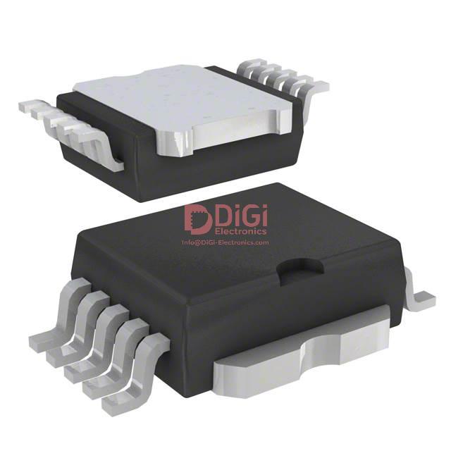
STMicroelectronics’ VIPER100ASP-E leverages the ECOPACK® compliant PowerSO-10 package, engineered for seamless integration into automated assembly. The package incorporates lead-free interconnects aligned with JEDEC JESD97, reducing environmental impact while maintaining robust electrical performance. PowerSO-10’s well-defined mechanical dimensions enable precise footprint generation in EDA tools, minimizing variance during pad design and component placement. Consistency in package sizing streamlines the DFM process, supporting repeatable soldering results across production runs.
Offering both tube and tape/reel shipping configurations ensures compatibility with high-throughput automated pick-and-place equipment. Tape/reel orientation precisely matches industrial feeders, optimizing cycle time and reducing component loss. Strategic decisions in supply logistics can directly influence SMT yield, especially when balancing storage conditions, feeder loading frequencies, and orientation tolerances on placement machinery.
Comprehensive mechanical documentation provided by STMicroelectronics assists in designing for manufacturability. For example, clear lead coplanarity and standoff specifications mitigate cold solder joints and tombstoning effects on PCB assemblies. Experience shows that maintaining recommended land-pattern geometries and stencil aperture ratios for PowerSO-10 ensures stable reflow profiles, resulting in uniform solder fillet formation and minimal voiding.
Underlying these practicalities, the packaging strategy for VIPER100ASP-E is a critical interface between silicon performance and board-level reliability. PowerSO-10’s thermal conductivity, combined with accurate pad design, supports efficient heat dissipation—vital in power management applications with high energy density. Reliable package-to-board connectivity is sustained not just by mechanical precision, but also by leveraging material compatibility and surface finish choices in downstream process engineering.
Integration of rigorous internal design rules and alignment with global standards confirms the package’s role as a foundation for yield optimization and long-term reliability in mass production environments, while proactively addressing sustainability objectives. Advanced understanding of these mechanisms empowers engineers to implement VIPER100ASP-E with confidence in demanding applications, resulting in robust circuit operation across diverse operating cycles.
Potential Equivalent/Replacement Models for VIPER100ASP-E
In power supply design, the selection of a suitable primary-side controller directly impacts system performance, reliability, and manufacturability. STMicroelectronics' VIPer series presents a robust family of integrated PWM controllers optimized for switch-mode power applications, with the VIPER100ASP-E and VIPER100A-E exemplifying close electrical and functional alignment. Both models integrate advanced control logic, high-voltage startup circuitry, and protective features, enabling streamlined designs for wide-ranging input voltages.
When a direct footprint-compatible substitute is needed for the VIPER100ASP-E, the VIPER100A-E emerges as the primary candidate. Its near-identical electrical parameters—including switching frequency, start-up characteristics, and maximum drain current—facilitate drop-in replacements in most topologies, particularly flyback or buck-boost configurations in consumer and industrial segments. Careful attention should be given to package outlines and thermal ratings; minor variations between "A" and "ASP" variants, such as differences in surge handling or case style, may influence PCB layout and thermal management strategies. Experience has shown that even subtle differences in package metallization can result in measurable long-term reliability shifts, especially in high-duty-cycle environments.
For applications where power ratings or functional demands exceed the VIPER100A-E’s envelope—such as higher output current, broader VDD operating ranges, or advanced soft-start functions—newer VIPer series controllers warrant close examination. Families like the VIPerPlus series extend functional integration, offering enhanced power efficiency, lower standby consumption, and improved EMI performance. Selection among these alternatives necessitates a fine-grained analysis of system needs, as advanced protection schemes or digital interface options in newer controllers can facilitate compliance with emerging regulatory and efficiency standards.
Vendor reference designs and parametric comparison tools serve as practical starting points, but benchmarking in the target system remains essential. Transient response, start-up overshoot, and fault recovery behaviors can differ even among controllers with similar datasheet parameters. Past substitution efforts have demonstrated the value of pre-qualification testing under elevated ambient conditions, revealing potential issues in switching losses or latch-up immunity not immediately obvious from datasheet cross-reference.
Long-term supply chain sustainability also plays a decisive role; evaluating product longevity roadmaps for the chosen model guards against obsolescence-driven redesigns. Regular engagement with manufacturer technical support can uncover silicon revisions or application-specific advisories, which may not be broadly documented yet can critically affect high-reliability or safety-compliant designs.
Ultimately, the process of selecting an alternative to the VIPER100ASP-E combines a thorough understanding of controller architectures, nuanced scrutiny of electrical footprints, and hands-on evaluation under realistic operating conditions. A methodical, forward-looking selection approach not only secures immediate functionality but contributes to lifecycle resilience and regulatory robustness in modern power applications.
Conclusion
The VIPER100ASP-E series from STMicroelectronics is engineered to address the advanced requirements of contemporary offline flyback power topologies. The core architecture integrates an adaptive control system, leveraging quasi-resonant and time-based regulation to optimize switching events in real time. This approach reduces conduction losses and mitigates electromagnetic interference, laying a solid foundation for energy efficiency in AC/DC conversion. The single-chip solution consolidates primary-side regulation, startup circuitry, and MOSFET power stage, thereby curtailing external component count and streamlining PCB layout. The system operates reliably in a wide input voltage range, ensuring consistent performance under both universal line conditions and brown-out scenarios.
Integrated energy-saving functions implement deep burst-mode and standby operations, enabling designers to meet stringent standby power directives without sacrificing dynamic response during load transitions. Advanced fault management encompasses overvoltage, overload, and thermal protection, employing autonomous shutdown and auto-retry logic to safeguard both the IC and peripheral circuitry against abnormal events. These robust features support sustained long-term reliability, crucial for mission-critical industrial controls and consumer applications.
From a design perspective, practical experience reveals that precise snubber network configuration and transformer selection can significantly enhance EMI compliance and efficiency. Equally important is meticulous PCB placement of high-frequency current loops around the VIPER100ASP-E package to minimize parasitic effects and ensure optimal thermal dissipation. The device’s holistic integration simplifies sourcing and logistics, reducing qualification cycles and overall BOM costs, while the programmable parameters facilitate tailoring to a broad spectrum of output requirements.
Applying the VIPER100ASP-E series in auxiliary power supply circuits for appliances, IoT gateways, and industrial automation platforms demonstrates substantial gains in performance-to-cost ratio. Adaptive switching control ensures stability under variable load conditions, and embedded protections minimize service disruptions—critical in field deployments with high reliability expectations. The ability to scale power architectures by design reuse expedites development timelines and simplifies certification.
Within the evolving landscape of power conversion, high-integration ICs such as the VIPER100ASP-E empower engineers to construct resilient, space-efficient solutions that align with environmental and regulatory demands. The platform’s thoughtful engineering, combined with adaptable feature sets, manifests as a strategic enabler for next-generation electronics ecosystems.


