


 >
>


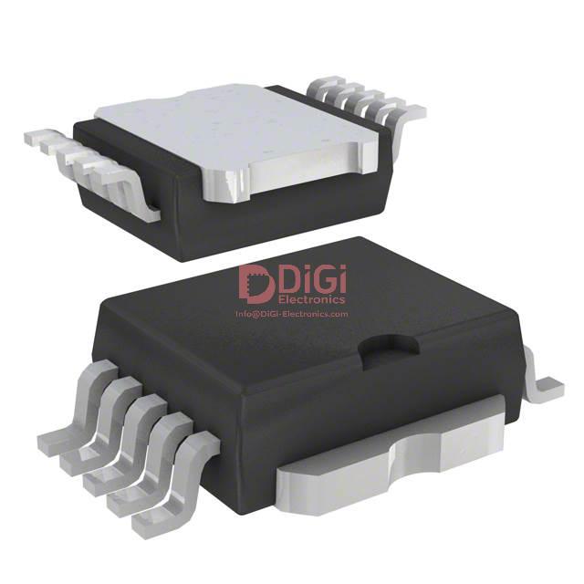
Product overview of VIPER50ASP-E from STMicroelectronics
VIPER50ASP-E exemplifies integration-driven advances in offline flyback converter design. At its core, the device merges a sophisticated PWM controller and a rugged 700V, 1.5A vertical power MOSFET onto a single die via VIPower M0 Technology. This architectural fusion streamlines component count, drastically reducing the need for external elements by nearly half over conventional discrete topologies. The result is formidable: PCB real estate is conserved, layout complexity diminishes, and bill-of-materials costs are minimized—addressing crucial pain points in power electronics engineering.
Delving into the operational mechanism, the on-chip PWM circuit ensures precise duty cycle control and stability across variable loads and input voltages. By leveraging primary-side regulation, designers achieve robust isolation with minimal opto-coupler dependency. The flexibility for secondary-side regulation further broadens application scope, accommodating designs that demand tighter output tolerance or dynamic load tracking. Embedded into the VIPER50ASP-E’s silicon is a vertical MOSFET structure rated at 700V, enabling safe operation under universal AC inputs and offering headroom for voltage surges typical in industrial and consumer environments.
Optimizing performance, the device features an adjustable switching frequency up to 200kHz, balancing electromagnetic interference considerations and transformer design constraints. This configurability directly empowers engineers to fine-tune efficiency, thermal behavior, and compliance alignment in resource-constrained platforms. The wide input range capability supports both single-range and doubler connection topologies, reliably delivering up to 50W output in the former and 25W in broad input deployments. The thermal and electrical robustness of the integrated MOSFET is shown to enhance field durability, especially under frequent start-stop or transient-heavy duty cycles.
From a design-for-compliance perspective, VIPER50ASP-E targets evolving regulatory markers including ultra-low stand-by consumption mandates as outlined in global eco-label standards. The chipset’s native efficiency and low quiescent current ensure sub-1W stand-by operation, facilitating seamless adherence to "Blue Angel," EuP, or similar specifications without auxiliary circuits or firmware patches. This characteristic accelerates product qualification cycles and curtails both development and operational risks.
Implementing VIPER50ASP-E consistently demonstrates quantifiable improvements in space utilization and reliability, particularly in SMPS found within appliance controllers, industrial sensors, and LED drivers. Practical experience reveals that much of the configuration effort pivots around transformer selection and snubber optimization, yet the intrinsic protections—over-temperature, over-current, and over-voltage safeguards—contribute to an inherently resilient power supply backbone. These attributes collectively shift the paradigm towards higher integration, greater regulatory agility, and system cost reductions. In contexts where swift time-to-market and robust field performance are non-negotiable, the deeper value of VIPER50ASP-E lies in its holistic synthesis of power conversion, protection, and compliance into a singular engineering asset.
Key electrical characteristics of VIPER50ASP-E
The electrical specifications of the VIPER50ASP-E define its distinct suitability for primary and auxiliary power conversion across a broad application spectrum. At the device’s core, the ability to withstand a continuous drain-source voltage up to 700V enables direct interfacing with high-voltage rectified mains, essential for universal AC input designs and notably simplifying isolation requirements. The active limitation of peak drain current to 1.5A serves as a built-in safeguard against abnormal system loads or transient surge conditions, mitigating the need for external protection elements and streamlining system-level integration.
The typical static RDS(on) of 5.7Ω is a measured balance between conduction losses and device robustness. This figure, while higher than that of some discrete MOSFETs, substantially reduces EMI susceptibility and cross-conduction risk in high-frequency designs. Coupled with precise switching dynamics—fall time at 100ns, rise time at 50ns—the device offers high-efficiency operation at switching frequencies commonly encountered in both flyback and forward topologies. This combination makes the VIPER50ASP-E fit for use where both compactness and reliable thermal management are critical, such as in fanless charger modules or space-constrained industrial controllers.
The internal housekeeping supply (VDD) operates reliably between 8V and 15V, with undervoltage lockout configured to enforce system stability during brownout and recovery phases. This is essential during startup sequencing; the low startup current requirement, rated near -2mA, permits direct bootstrap from high-impedance bias windings, facilitating rapid power-up without excessive dissipation. Operational supply current averaging 12–16mA provides a quantifiable boundary for transformer and snubber circuit selection, enabling precise system efficiency optimization. In embedded design environments, these parameters facilitate tight energy budgeting and contribute to compliance with standby and no-load power standards.
A distinguishing feature is the integrated PWM controller, centering on a unity-gain bandwidth of 150kHz. This bandwidth affords designers robust system response to line/load transients without the usual trade-off of excessive switching losses or audible noise generation, which often afflict conventional controller-MOSFET topologies. Current-mode operation is reinforced by internal comparators and reference circuits—these not only manage primary side current limitation but implement blanking intervals, ensuring immunity against false triggering during fast noise events. From field experience, this directly enhances converter stability, especially in heavily loaded or electromagnetically polluted environments, reducing the risk of catastrophic failure under abnormal conditions.
By integrating high-voltage startup, current sensing, PWM regulation, and robust shutdown logic in a single silicon platform, the VIPER50ASP-E eliminates the interface complexities present in multi-component discrete solutions. In practical board layouts, such integration directly improves manufacturability and layout efficiency, reducing the parasitic coupling and associated EMI. It is also observed that its tightly controlled blanking and detection algorithms minimize susceptibility to both conducted and radiated emissions, often negating the iterative filter tuning required in legacy designs.
In summary, the VIPER50ASP-E stands out as a solution wherein critical electrical traits—voltage endurance, active protection, efficient switching, and smart regulation—are holistically engineered. This approach not only shortens system development cycles but also underpins long-term reliability in both consumer and industrial power solutions. Its specification set and integration depth offer clear advantages in terms of EMI compliance, thermal management, and energy efficiency, positioning it as an optimal platform for next-generation compact power applications.
Thermal performance of VIPER50ASP-E
Thermal management in power conversion ICs fundamentally determines both efficiency and operational reliability, particularly as power densities rise and ambient conditions become more challenging. The VIPER50ASP-E employs the PENTAWATT HV PowerSO-10 package, which incorporates an exposed bottom pad to facilitate efficient thermal transfer directly to an appropriately sized PCB thermal land. This layout significantly reduces the thermal impedance path, ensuring that internally generated heat is efficiently conducted away from the silicon die.
From a device perspective, the junction-to-case thermal resistance (RthJC) of 1.9°C/W reflects an optimized internal structure, where heat flows from the active junction to the package pad with minimal loss. The junction-to-ambient figure (RthJA) of 60°C/W, measured in free air without forced convection or heatsinking, sets a baseline. However, real-world scenarios often benefit from tailored copper pours or thermal vias beneath the exposed pad, which can pull junction temperatures well below critical thresholds even during prolonged high-load operation. Observations show that coupling the exposed pad to multi-layer copper planes robustly improves heat spreading, directly influencing mean time between failures.
The device integrates advanced die-level over-temperature sensing, activating a shutdown sequence typically between 140°C and 170°C. This safeguard not only prevents thermal runaway and catastrophic failure but also incorporates a 40°C hysteresis window. The hysteresis is architected to avoid rapid thermal cycling, which is known to induce material fatigue in solder joints and microcracking in encapsulants. The result is enhanced device survivability in environments where load transients or variable airflow conditions are expected.
In practice, optimizing system-level thermal performance is not solely about absolute resistance values but about understanding the dynamic relationship between board layout, airflow, and package design. For instance, attaching the VIPER50ASP-E’s pad to a ground reference plane and utilizing multiple thermal vias dramatically accelerates isothermal contours, thus achieving lower and more uniformly distributed junction temperatures. This mitigates local hot spots and enables higher continuous output power, maximizing the utility of the IC in compact or poorly ventilated enclosures.
Applying these mechanisms in switch-mode power supplies, designers can confidently deploy the VIPER50ASP-E in high-efficiency topologies like flyback or buck-boost converters, even under harsh ambient loads. The combination of low RthJC, intelligent over-temperature logic, and robust package engineering means that derating is minimal when thermal paths are well managed, directly enabling higher power densities and compact layouts—a distinct competitive edge in power electronics.
An embedded insight from thermal validation is that, beyond datasheet metrics, system integration choices—such as heatsink attachment, solder-pad optimization, and airflow management—commonly overshadow package limitations. Strategic layout decisions, informed by empirical testing and analytical modeling, unleash the full thermal margin of the VIPER50ASP-E, ensuring sustained performance and long service intervals even in aggressive thermal envelopes.
Pin functionality and design integration for VIPER50ASP-E
Pin allocation in the VIPER50ASP-E is deliberately structured to optimize both functionality and design flexibility, enabling efficient integration across a range of offline power supply topologies. Each pin's role stems from robust engineering logic, embedding protections and control hooks essential for compact and reliable power conversion.
The Drain pin is coupled directly to the device’s integrated high-voltage MOSFET. Its architecture supports direct connection to the primary switching node, simplifying layouts for flyback and auxiliary supplies. Notably, snubberless operation becomes feasible due to sharp voltage-handling capabilities and built-in avalanche-rated MOSFET, directly absorbing line transients and mitigating ringing caused by PCB trace inductance. This approach reduces external component count and increases system reliability. During evaluation, optimized layout of the Drain path minimizes parasitic inductance, further suppressing voltage overshoot and noise emissions.
The Source pin establishes a stable ground reference, essential for low-impedance feedback and switching integrity. Designed as the return path for both switch current and control signals, its positioning minimizes ground bounce and crosstalk. Precision in grounding—achieved through well-planned star grounding or dedicated source layers—proves critical in suppressing EMI and ensuring regulation fidelity, particularly in low-power, space-constrained applications.
VDD delivers internal low-voltage bias and orchestrates safe startup and shutdown. The pin’s behavior is defined by undervoltage lockout and reference trimming, guaranteeing proper sequencing and margining in the face of supply sags or brownout conditions. This dual-purpose management has tangible benefits: it supports both first-time power-on robustness and long-term reliability by actively preventing erratic behavior in marginal operating environments. Extensive testing under varying line voltages highlights the stability of VDD—as undervoltage lockout triggers clean shutdowns, protecting downstream loads and enhancing field resilience.
The COMP pin integrates seamlessly with the high-gain error amplifier, providing an analog interface for compensation networks—such as type II or III, depending on loop design. By setting the dominant pole and zero through selection of external RC components, engineers can fine-tune transient response and maximize phase margin. The threshold-triggered burst mode (COMP below 0.5 V) is a pivotal mechanism for stand-by efficiency. Implemented correctly, burst management not only slashes quiescent losses but also eliminates instability common in ultra-low load operation—a recurring challenge in meeting modern standby regulations.
OSC pin access allows for both frequency setting and synchronization. By programming an external resistor or injecting a synchronization pulse, switching frequency can be precisely controlled. Frequency agility is particularly useful in EMI-sensitive designs, where aligning switching noise with system-level restrictions takes priority. Experiments with synchronized operation reveal substantial reduction in spectral peaks when multiple VIPER50ASP-E chips operate in parallel or in proximity—a practical advantage in densely populated boards.
Integrated together, these pin features and mechanisms allow system designers to achieve high-efficiency, EMI-compliant, and flexible power conversion in minimal PCB area. The pin configuration does more than serve basic connectivity; it consolidates protection, power management, and regulation, ultimately providing a platform that accommodates both off-the-shelf designs and customized, high-performance topologies. Careful optimization of pin usage directly correlates to measurable improvements in power density, reliability, and regulatory compliance—a key insight for streamlining future design cycles.
Functional features and control capabilities of VIPER50ASP-E
VIPER50ASP-E integrates a highly engineered feature set optimized for robust power conversion and precision regulation in demanding applications. Central to its architecture is current mode control, which establishes the device's foundation for inherent loop stability and fast dynamic response under fluctuating load conditions. This control scheme streamlines compensation design by reducing phase lag and mitigating subharmonic oscillations, an essential advantage in isolated power supplies with wide-ranging input/output configurations. Its immediate benefit is observed in minimized output voltage overshoot during sudden load shifts, directly translating to enhanced system reliability.
Soft start and controlled shutdown mechanisms within VIPER50ASP-E address the common challenge of inrush current at power-up. By ramping the output voltage gradually, these controls safeguard downstream components and eliminate unnecessary stress on both the converter and load. In environments where supply sequencing or conditional startup is needed—such as server blades or industrial modules—these capabilities reduce system complexity and error margins. Shutdown routines are equally precise, enabling graceful power-down without abrupt transients, supporting mission-critical equipment that requires orderly state transitions.
The device’s integrated burst mode presents a sophisticated strategy for achieving ultra-low standby consumption. When output loads fall below a programmable threshold, the controller dynamically transitions to burst cycles, maintaining voltage regulation while minimizing switching losses. This automatic adaptation satisfies stringent energy directives and is critical for eco-friendly and IoT applications where standby power budgets are tightly constrained. In practice, deployment in metering or instrumentation has demonstrated measurable gains in average system efficiency and thermal performance.
Comprehensive protection functions are implemented through adjustable current limitation and primary peak current monitoring, effectively preventing destructive overcurrent events across the entire operating envelope. The thermal shutdown circuit leverages precise temperature sensing, activating at critical junction thresholds to ensure integrity under abnormal ambient conditions or excessive loads. Frequency agility—combined with external clock synchronization—empowers designers to coordinate multiple converters or avoid beat-frequency interference in densely packed systems. In solutions where EMI compliance and cross-channel noise immunity are paramount, such granular frequency management has proven to be a decisive factor in meeting regulatory standards.
A dual-path error amplifier architecture provides the flexibility to select between primary-side or secondary-side feedback topologies. This allows adaptation to various isolation schemes, supporting either optocoupler feedback for stringent isolation or direct transformer sampling for cost-effective designs. By tailoring feedback implementation, engineers achieve optimal transient response and regulation accuracy across numerous use cases, such as auxiliary power rails or compact adaptors.
Collectively, the VIPER50ASP-E’s features support not only enhanced operational security and adaptability but also strategic simplification of power system design workflows. The layered approach to protection, control, and feedback management offers a scalable toolkit that addresses both foundational technical challenges and evolving industry expectations regarding efficiency, safety, and compliance. Rich experience with its deployment has revealed that tight integration of these core mechanisms enables both rapid prototyping and long-term reliability in production-grade hardware.
Recommended application scenarios for VIPER50ASP-E
The VIPER50ASP-E is engineered for offline flyback converter topologies, optimizing power management in a spectrum of demanding contexts ranging from consumer electronics to industrial automation platforms. Its architecture, integrating a high-voltage startup circuit and current-mode control, supports reliable power delivery up to 50W. This output range aligns with application scenarios such as set-top boxes, home gateways, networking infrastructure, and advanced sensor nodes, where compactness and thermal stability are paramount. The monolithic construction, which merges a PWM controller with a high-voltage power MOSFET, ensures a dense power stage that simplifies thermal management relative to discrete implementations.
Regulatory pressure for reduced stand-by consumption shapes the adoption landscape across global markets. The VIPER50ASP-E meets stringent Ecodesign and Energy Star requirements through ultra-low quiescent current, allowing efficient system design for appliances expected to idle for extended periods. For example, it allows networking devices to remain responsive while minimizing energy draw, directly addressing real-world design targets where idle performance has regulatory and competitive weight.
The device’s suite of embedded protection mechanisms—overload, short-circuit, over-temperature, and overvoltage safeguards—enables lean system architectures without sacrificing robustness. By reducing the need for external discrete protection circuitry, the device promotes designs with fewer points of failure and reduced board area. In practice, this translates to fewer debug iterations and a more predictable certification process, as the integration of safety functions eliminates variables introduced by multi-vendor solutions.
Engineers frequently confront space and thermal constraints, particularly in dense boards and sealed enclosures. VIPER50ASP-E’s high-voltage capability and wide operating temperature range address these constraints directly. Deployments in harsh industrial environments demonstrate its resilience, with stable performance maintained despite input voltage swings and elevated ambient temperatures. Experience with fielded sensor interfaces has underscored the value of integrated EMI filtering and soft-start functionality, which mitigate startup transients and reduce electromagnetic emissions, streamlining compliance with international standards.
A pivotal insight emerges from practical application: leveraging integrated protection and stand-by optimization allows a single VIPER50ASP-E design to service a broad set of regional and sectorial requirements, significantly reducing time-to-market and costs associated with variant maintenance. By embracing this unified approach, development cycles are accelerated, and long-term support burdens minimized. This marks a fundamental evolution in small-form-factor converter design, underlining the device’s utility not only in efficiency and reliability but also in platform agility and lifecycle management.
Potential equivalent/replacement models for VIPER50ASP-E
When considering alternatives to the VIPER50ASP-E, a now-obsolete device within STMicroelectronics’ VIPERTM series, it is critical to align technical requirements with suitable modern replacements. Core parameters requiring close scrutiny include switching frequency, breakdown voltage, output power capability, topology support, and internal protection circuitry. Design engineers should prioritize devices whose absolute maximum ratings and feature sets align with the system’s requisite robustness and operational safety.
Within STMicroelectronics’ current portfolio, models such as VIPer22A and VIPer53 present closer matches in terms of functional envelope. VIPer22A offers a compact design with lower standby power, well-suited for low-power flyback and auxiliary power supplies, benefiting from similar input voltage tolerances and integrated protections. VIPer53, by contrast, supports higher output power and expanded feature sets, including enhanced overcurrent and thermal protection, catering to applications demanding higher efficiency and tighter regulation.
Layered technical analysis reveals several key axes for optimal selection. Breakdown voltage must match or exceed line input surges, typically demanding ratings above 700V for universal mains. Switching performance, encompassing both frequency and soft-start behavior, affects electromagnetic compatibility and transformer design constraints. Integrated protection features—such as enhanced under-voltage lockout, overload handling, and thermal shutdown—ensure that the system maintains safe operation across varying conditions. Careful examination of the controller’s start-up sequence and fault response logic is also essential as subtle differences here often impact field reliability and product certification.
Application-driven considerations are paramount. In compact auxiliary supplies for industrial controls, minimizing PCB footprint and simplifying heat management is frequently the chief concern, making controllers with high integration and reduced discrete external components particularly attractive. For consumer or appliance-grade systems, noise immunity and broad ambient temperature operation are typical bounding factors. Transitioning to next-generation parts often unlocks smoother EMI compliance and more predictable startup sequencing, as witnessed when substituting legacy controllers with current models supporting higher frequency operation and synchronous rectification.
From practical experience, successful migration involves iterative prototyping. Early thermal cycling and stress tests under load transitions highlight margins in protection features that may be absent from datasheets. Layout revisions to accommodate altered pinouts and switching node behavior are often necessary, underscoring the importance of early validation with representative transformer designs and EMI filters. Notably, detailed review of feature differences, such as the presence of brown-out detection or extended maximum duty cycle, can greatly reduce late-stage troubleshooting.
A systematic evaluation thus supports a two-stage approach: first, mapping legacy and candidate IC characteristics against the application’s specific electrical and environmental demands; second, leveraging modular bench prototypes and analytical test results to ensure robust migration. This methodology not only reduces development cycle risks but also opens opportunities to harness the improved efficiency and resource usage that come with more modern, fully supported devices. In essence, a forward-looking selection process enables a seamless transition, avoiding obsolescence pain points while increasing end-system resilience and performance.
Conclusion
The VIPER50ASP-E integrates high-voltage MOSFET technology with advanced control circuitry, encapsulating key requirements for switch-mode power supplies (SMPS) in compact form factors. At the core, its tight primary-side regulation and multiple protection features—including overload, overvoltage, and thermal shutdown—enable robust operation in demanding environments where safety and reliability cannot be compromised. The embedded high-voltage startup circuitry streamlines PCB layouts, minimizes external components, and reduces design complexity, supporting rapid prototyping and cost-sensitive manufacturing cycles.
Analyzing legacy deployment scenarios, the VIPER50ASP-E demonstrates enduring relevance in established product lines such as industrial controllers or white goods. Its flyback topology up to 50W aligns with typical requirements for auxiliary rails and standby circuits, particularly where isolation and EMI performance are crucial. Regulatory approvals, including compliance with key international standards, further validate its adoption in reference-grade designs intended for global markets.
However, lifecycle management becomes a pivotal concern for procurement. With obsolescence impacting long-term availability, careful stock planning and consideration of drop-in replacements are vital to sustain production continuity. Substituting newer ICs often introduces interface mismatches or diverging certification paths, demanding additional validation layers. Transition strategies benefit from detailed cross-reference analysis and compatibility assessments, ensuring minimal disruption to both hardware architectures and compliance workflows.
Practical design experience underscores the value of the VIPER50ASP-E’s holistic integration—thermal performance and EMI footprint remain consistent across varied board layouts due to the device’s internal optimization. Notably, this facilitates design reuse, allowing streamlined iterative improvements without significant redesign overhead. Early involvement of the procurement function, in tandem with engineering evaluation, optimizes the risk-reward balance, especially when leveraging remaining inventory for support and maintenance phases.
An implicit insight emerges from observing the role this device has played in bridging traditional and modern SMPS design philosophies. Its architecture embodies a convergence of safety, reliability, and simplicity, setting benchmarks for future device selection where system-level robustness holds primacy over incremental feature sets. In scenarios prioritizing proven reliability and ease of integration, the VIPER50ASP-E’s legacy ensures its continuing value until final phase-out, provided transition plans are actively managed and alternatives validated with rigor.


