 >
>


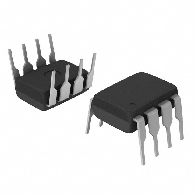
Product overview of the VIPER53SP series from STMicroelectronics
The VIPER53SP series from STMicroelectronics embodies a high-performance solution for offline flyback power conversion, engineered to meet stringent reliability and efficiency standards in primary-side switched-mode power supply design. At its core, the integration of a 620V-rated internal power MOSFET optimizes voltage endurance and switching dynamics, crucial for maintaining stability under line transients and minimizing component stress. This architecture circumvents the traditional need for discrete high-voltage FETs, reducing both board space and parasitic losses inherent in modular topologies.
The flyback topology supported by VIPER53SP leverages precise switching control, with the IC achieving up to 300kHz operation. This high-frequency capability not only facilitates the reduction of magnetic component sizes, leading to more compact designs, but also supports rapid transient response—a critical parameter in systems where output regulation during load changes is mandatory. The on-chip oscillator and driver circuitry are tuned for low propagation delay and jitter, ensuring predictable switching behavior and minimizing EMI generation.
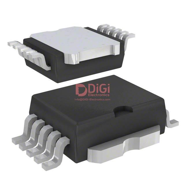
Thermal management is addressed through the PowerSO-10 exposed-pad package, delivering a path for efficient heat dissipation. In dense SMPS layouts, this feature is pivotal for sustaining extended operation at elevated ambient temperatures, particularly when driving loads with variable or high current demands. Engineering experience demonstrates that judicious layout practices exploiting the exposed pad can notably decrease thermal resistance, thus enabling higher continuous output power without derating.
Comprehensive protection circuits embedded within the VIPER53SP form the basis for robust SMPS design. These include cycle-by-cycle current limitation, overvoltage protection, thermal shutdown, and an auto-restart mode for fault recovery. The integrated nature of these protections simplifies design validation and contributes to faster regulatory compliance, as failure modes can be tightly constrained within predictable bounds. Practical deployment often reveals that such built-in protections reduce the need for external supervisory ICs, streamlining both the BOM and certification process.
VIPER53SP’s application range extends into compact adapters, auxiliary power supplies, industrial controllers, and home electronics—domains where conversion efficacy, low idle power, and form factor are decisive. Real-world optimization frequently involves the synergy between its high-voltage MOSFET and peak current mode control, fostering low standby consumption and supporting global energy standards. The device’s ability to sustain operation over wide input voltages aligns with demanding international deployment scenarios.
The architecture also subtly incorporates noise management considerations. The high-voltage MOSFET’s fast switching, balanced with tailored gate control, allows for minimized switching losses and superior interference management, a foundational requirement for circuit compliance with EMC norms. Strategic snubber and filter design, informed by the integrated protections and switching profile, further enhances system noise immunity and efficiency.
Designers leveraging VIPER53SP realize strategic benefits in reducing development cycles and achieving consistent power conversion across use cases. The cohesiveness of integration, protection, and thermal performance forms a practical axis for high-density SMPS layouts. Experience confirms that mastery of PCB layout—specifically optimizing thermal paths and minimizing noise-sensitive loops—unlocks the full capabilities of the VIPER53SP series in power electronics applications.
Key features and functional advantages of the VIPER53SP
The VIPER53SP exemplifies a nuanced approach to integrated power supply design, particularly in demanding applications requiring both isolation and high efficiency. Its fundamental architecture leverages a flyback topology incorporating a high-voltage MDmesh™ MOSFET directly within the chip package. This level of integration significantly reduces external component count and corresponding PCB real estate, streamlining both prototyping and mass production cycles. Moreover, the embedded primary-side switching and output isolation circuitry lower the barrier for achieving IEC and UL compliance, as isolation margins become easier to control and verify during both simulation and end-of-line testing.
Underlying the control implementation, the device supports precise frequency tuning via a dedicated oscillator pin. In practice, the flexibility to define the switching frequency up to 300kHz with a simple RC network enables optimization tailored to specific EMI constraints or thermal environments. For example, frequencies can be shifted to avoid regulatory test bands or to dampen noise coupling onto vulnerable signal lines—an increasingly valuable capability in densely populated power management boards. Additionally, frequency adjustment offers tangible benefits when matched to magnetic core and transformer design, supporting maximum efficiency across wide dynamic load ranges.
The suite of protective features embedded in the VIPER53SP reflects a comprehensive risk mitigation strategy. Its current-mode control loop not only bolsters transient performance but also allows for programmable peak current limits—critical when operating near transformer saturation or when secondary side loads exhibit inrush characteristics. The presence of hysteretic undervoltage lockout and configurable overload reset further improves system reliability, preventing oscillatory faults while minimizing downtime. Experience shows these features reduce the likelihood of latent field failures, enhancing the predictability of both soft and hard shutdown events.
Power savings during periods of low load are addressed by an automatic burst mode mechanism, which is seamlessly activated to keep standby consumption at an absolute minimum. This automated transition between active and burst states supports competitiveness in segments governed by the latest efficiency protocols such as DOE Level VI or EU Ecodesign. In mature power architectures, integrating this feature often eliminates the need for auxiliary circuits, thereby simplifying bill-of-materials management and accelerating design qualification for energy-sensitive end products.
At initial power-up, the VIPER53SP employs a built-in high-voltage current source, which reliably charges the VDD rail—eliminating common startup lag or variability tied to external bias supplies. A high-gain error amplifier forms the centerpiece of the regulation loop, capable of stabilizing output across various compensation schemes. Both optocoupler-based secondary feedback and resistive primary feedback are well supported, offering design latitude for diverse isolation classes or application requirements. During practical evaluation, this robustness frequently translates into low output ripple and swift transient recovery, even under highly variable loads—key for applications in industrial controls, instrumentation, and consumer adapters.
Advancing beyond basic integration, the distinctive capabilities of the VIPER53SP underscore the value of converging control flexibility, application-focused protections, and energy management within a single monolithic device. By addressing layout efficiency, compliance thresholds, and operational resilience within one compact package, it enables shorter design cycles and superior long-term reliability—factors that increasingly define competitiveness in professional-grade power solutions.
Electrical characteristics and performance details of the VIPER53SP
When analyzing the VIPER53SP, it is essential to focus on its integrated high-voltage MOSFET and control circuitry, which together enable both robustness and flexibility in offline power supply topologies. The device’s absolute maximum ratings reflect the integration approach: the 620V drain-source tolerance enables use in direct rectified European or universal mains, greatly simplifying primary-side design for isolated flyback and buck-boost converters. The supported VDD range (8.4V to 19V) covers the necessary startup and steady-state operating conditions, ensuring compatibility with common bias supply arrangements or auxiliary winding approaches.
Careful attention should be paid to output power constraints, which are influenced not only by silicon limitations but also by package thermal impedance and board-level heat dissipation. For the PowerSO-10 package, achieving 65W output under 195–265VAC input is feasible if PCB copper area, airflow, and layout are optimized for thermal transfer. Under universal input conditions, designers must account for elevated conduction and switching losses at lower line voltages, which typically restricts output to 40W unless additional cooling measures are implemented. This interplay between electrical limits and thermal engineering underlines the necessity for early-stage thermal simulation and strategic PCB copper area reservation during layout.
The VIPER53SP’s conduction efficiency is anchored by its low RDS(on) MOSFET, providing a 1Ω typical value at 25°C. This allows for modest losses during on-state conduction, which becomes increasingly important at lower output voltages or higher output currents. Fast transistor switching—with 50ns rise and 100ns fall times—minimizes switching losses and reduces the time in high dissipation zones, making high-frequency topologies practical. Such characteristics facilitate tight transformer design and smaller magnetics, but impose strict requirements on PCB trace impedance and snubber design to avoid voltage overshoot and EMI spikes.
Precision regulation in demanding loads is handled by a high-gain (45dB) error amplifier with a 700kHz bandwidth, characteristics that support both tight output voltage regulation and rapid throughput of line/load disturbance corrections. Real-world experience indicates that loop compensation should be considered early in the design; a 10nF minimum capacitance on the COMP pin will stabilize the loop across operating conditions, but fine-tuning this value based on output capacitance, optocoupler response, and system bandwidth can further enhance transient behavior and noise immunity. Robust compensation and loop design allow the device to meet strict industrial and consumer appliance regulatory requirements under varying load profiles.
Oscillator frequency accuracy within ±5% ensures repeatable EMI performance and minimizes challenges during compliance testing and manufacturing duplication. This stability reduces the drift in EMI spectra that often complicates mass production. In systems where conducted and radiated emissions are critical, frequency spread and synchronization to system clocks can be considered, utilizing the predictable oscillator as a reference point for advanced filter design.
A nuanced aspect lies in balancing efficiency, thermals, and regulation; highly efficient operation often shifts thermal load to specific PCB areas, magnifying the importance of copper shapes and vias beneath the PowerSO-10 pad. In production, monitoring for variation in switching characteristics and verifying regulation under worst-case line/load transients are key to high-yield results.
Strategically, the VIPER53SP provides a unified platform for power conversion in appliances, industrial controls, and LED drivers, where high integration reduces BOM count and manufacturing complexity. Leveraging its robust switching and control, designers can iterate rapidly from breadboard to production, provided early attention is given to layout, thermal design, and loop stability. An often-overlooked insight is that the system-level efficiency and EMC profile are dictated as much by layout and compensation as by the silicon itself; disciplined engineering practices in these areas consistently differentiate top-performing designs.
Application scenarios and design considerations for the VIPER53SP
The VIPER53SP is engineered for isolated, off-line power supply solutions across a broad spectrum: from auxiliary rails in white goods and industrial drives to standby provisioning in networking equipment and compact adapters for consumer devices. High integration—encompassing PWM controller, power MOSFET, and key protection circuitry—significantly reduces external component count, shrinking overall footprint and simplifying PCB layouts. This streamlining directly benefits designs targeting low- to mid-power outputs, where system cost and reliability play pivotal roles. Versatile constant-current/constant-voltage regulation provides seamless adaptation to diverse loads, such as Li-ion cell chargers and USB power modules, aligning with fluctuating commercial demands for universal applicability.
Correct system sizing hinges on a thorough understanding of the interplay between package thermal limitations, line input conditions, and end-use thermal environments. For PowerSO-10 packages, leveraging the full 65W output at nominal 230VAC input is feasible under favorable airflow and board layout scenarios, but practical designs must account for derating. Universal mains operation—exposing the system to 85–265VAC—necessitates a conservative approach, particularly under high ambient or restricted cooling. Empirical validation often reveals subtle derating thresholds not captured in datasheets, underscoring the value of iterative prototype thermal profiling and margin analysis. Preemptive adjustment of design targets mitigates the risk of latent failures or premature aging in high-density enclosures.
Mitigating operational hazards requires carefully orchestrated use of integrated and external protections. Tuning the TOVL (Threshold Overload) pin with an external RC network enables precise control over overload response, allowing tailored ride-through or latching shutdown appropriate to specific loads and safety norms. The synergy of built-in undervoltage lockout, overtemperature protection, and delayed fault shut-down forms a robust defense against fluctuating line conditions, overheated environments, or downstream shorts. In practice, redundancy in protection—combining hardware thresholds with firmware monitoring for smart applications—enhances overall MTBF estimates, a valuable metric in critical industrial or mission-critical infrastructure.
Frequency management represents another axis for system-level optimization. The locally programmable oscillator offers granular EMI tuning; lowering the operating frequency typically reduces radiated and conducted emissions—a necessity for compliance with stringent CE/FCC standards in noise-sensitive environments. Conversely, pushing frequency higher enables reductions in transformer core size and winding losses, a strategy favored in space-constrained or thermally aggressive designs, provided thermal headroom is preserved. Prototypes often benefit from iterative frequency sweeps, supported by near-field EMI scanning and infrared imaging, to uncover optimal trade-offs unique to each form factor or enclosure.
The VIPER53SP thus provides a flexible platform for optimizing isolated power supplies under diverse operational regimes, balancing form factor, thermal constraints, noise targets, and protection demands. Subtle design refinements—grounded in iterative prototyping and real-world application data—unlock its full potential across both traditional and emerging electronic ecosystems. The device’s architecture enables systematic risk control and efficiency tuning, streamlining certification while accommodating innovation in end equipment design.
Thermal performance and package information for the VIPER53SP
Thermal characteristics serve as a critical determinant in maximising output power and operational stability for integrated circuits such as the VIPER53SP. The PowerSO-10 package offers an engineered balance between compactness and thermal management, presenting a junction-to-case thermal resistance (RθJC) of 2°C/W, and junction-to-ambient (RθJA) of 60°C/W under conditions of sufficient copper heat-sinking. These values form the boundary conditions for predictable thermal performance.
The exposed pad feature, integral to the package, is designed for optimal thermal coupling with the PCB. Direct contact with a well-dimensioned thermal plane enables efficient transfer of heat away from the junction, yielding substantial reductions in device operating temperatures. Applying broad copper areas beneath the drain and source pins further amplifies this effect. Empirical observations confirm that isolating these copper pours, free from unnecessary signal traces or via interruption, enhances overall thermal flow and supports sustained high-output operation under elevated load conditions.
Strategic PCB layout becomes indispensable when approaching output power limits or operating in environments with restricted airflow. The construction of thermal paths through careful via placement, thickness selection, and strategic layering ensures uniform temperature distribution, minimizing hotspots and their associated risks. Designs that prioritize thermal continuity from the exposed pad into the ground or power plane exhibit improved longevity and maintain consistent electrical characteristics over time.
Within the stipulated –40°C to +150°C case temperature envelope, operational reliability is favored by reducing the delta between junction and ambient, especially in high-power or pulsed scenarios. Integrating simulations with real-world PCB prototypes clarifies how minor increases in copper area or adjustments of pad shapes can yield measurable improvements in thermal dissipation. These iterative refinements allow the device to operate comfortably below thermal derating thresholds, maintaining robust electrical performance even in thermally stressful installations.
One prevailing insight is the asymmetry of thermal resistance across package interfaces. Focusing heat extraction at the case-to-ambient boundary, rather than solely at the junction-to-case, produces more tangible gains for compact systems. This underscores the necessity of aligning mechanical mounting decisions and PCB design parameters to maximize the PowerSO-10 package's inherent strengths in real deployment scenarios. The nuanced interplay between package features and board-level thermal strategies ultimately defines the achievable envelope for power, efficiency, and reliability.
Potential equivalent/replacement models for the VIPER53SP series
The transition from the VIPER53SP series to alternative power management ICs necessitates meticulous evaluation of both electrical and application-level parameters. Central to this process is the matching of internal MOSFET ratings—voltage tolerance and continuous drain current must directly map to load requirements and topology constraints within the targeted system. Devices such as the VIPER22A and VIPER12A present viable options within STMicroelectronics’ VIPer™ portfolio, given their comparable high-voltage robustness and configurable switching capabilities, though subtle disparities in maximum drain-source voltage or switching current tolerances may drive selection for either low-power or robust supply rails.
Pin-to-pin compatibility is not merely a matter of schematic substitution. Thermal characteristics and pad layouts profoundly affect assembly yield and in-field reliability. In practice, successful cross-reference depends on overlaying package drawings and verifying footprint match against the existing PCB; slight misalignment, even on seemingly minor pin functions such as feedback or enable, can trigger system-level failures if overlooked. Field experience routinely shows that spacing, isolation, and pin orientation often demand iterative revision in CAD tools—especially when aligning with legacy thermal dissipation profiles.
Features common to the VIPER53SP, such as programmable switching frequency and comprehensive protection mechanisms—overvoltage, overload, and thermal shutdown—must be appraised in replacement candidates. The newer VIPer™ generation introduces both analog and digital programmability options, making it imperative to scrutinize datasheet timing diagrams and logic thresholds for compatibility with upstream control signals. While standby operation and low quiescent current have become standard, nuanced differences in trigger points or soft-start routines can affect EMI signatures and regulator startup behavior, necessitating bench validation in prototype assemblies.
Regulatory and supply chain parameters are increasingly determinative for long-term deployment. RoHS and REACH compliance are baseline requirements, but practical assurance of lifecycle support hinges on vendor commitment to not just regulatory certification, but also stable forecasted availability. Anecdotal evidence suggests that designs based on newer VIPer™ variants better withstand component shortages due to broader distributor stock; this advantage becomes material for high-volume or time-sensitive projects.
Applying these layered criteria leads to a more resilient power conversion subsystem architecture. The ideal replacement for VIPER53SP is not solely a matter of drop-in electrical parity, but rather achieving systemic reliability through modern packaging, robust protection features, and proven lifecycle support. In situations where direct substitution is impracticable, leveraging enhanced programmability and thermal efficiency of newer VIPer™ devices empowers iterative board spins and product refresh cycles without extensive requalification. Insightful selection combines thorough datasheet analysis with empirical prototype testing, optimizing the balance between technical fidelity, manufacturing practicality, and product longevity.
Conclusion
The VIPER53SP series from STMicroelectronics exemplifies a high degree of integration in offline flyback converter architecture, leveraging an embedded MOSFET to streamline design while maintaining stringent safety and protection features. Core circuit elements are designed to withstand transient overloads, with built-in protections against overvoltage, undervoltage, and thermal excess. The topology enables direct coupling with primary-side regulation schemes, minimizing external component count and simplifying PCBA layouts for medium-power platforms. Notably, the integrated start-up control and restart logic optimize no-load and light-load behaviors, supporting system reliability and regulatory conformance in energy-saving contexts.
Device interoperability hinges on careful attention to parameters such as gate drive timing, current sense thresholds, and switching frequencies. When mapping the VIPER53SP against contemporary alternatives, matching Rds(on) and breakdown voltage values ensures compatibility with legacy magnetic and passive components, streamlining drop-in upgrades. Application scenarios typically include industrial control modules, utility metering, and consumer adaptors where EMI constraints and Creepage/Clearance requirements are pronounced. The product’s historical deployment demonstrates that minimizing parasitic elements and maintaining thermal margins can enhance operational lifespan, particularly in wide-range input environments subject to voltage surges and brownout conditions.
Transitioning to modern replacements necessitates a comprehensive review of evolving safety protocols, such as reinforced isolation and fault reporting standards seen in IEC 62368-1 and DOE Level VI efficiency marks. Selection strategies should address both feature continuity—like brownout immunity or low standby draw—and component supply chain robustness to avoid redesign cycles. Practical deployment experience shows that leveraging auto-restart and frequency jitter functions enables greater tolerance to line noise and variable load conditions, directly reducing field failure rates.
Analyzing market shifts, integrated switch-mode controllers increasingly incorporate digital configuration interfaces and higher dV/dt robustness, a trend forecasted to drive adoption in interconnected IoT power nodes. Organic assessment of VIPER53SP migratory paths reveals a bias toward multi-functionality, suggesting that future-proofing power architecture relies not only on matching electrical specification but also on anticipating standards evolution and diagnostic capabilities. Layering enhanced diagnostics and adaptive feedback into the primary switching domain unlocks value, fostering maintainable and scalable power designs in emerging application spaces.