 >
>


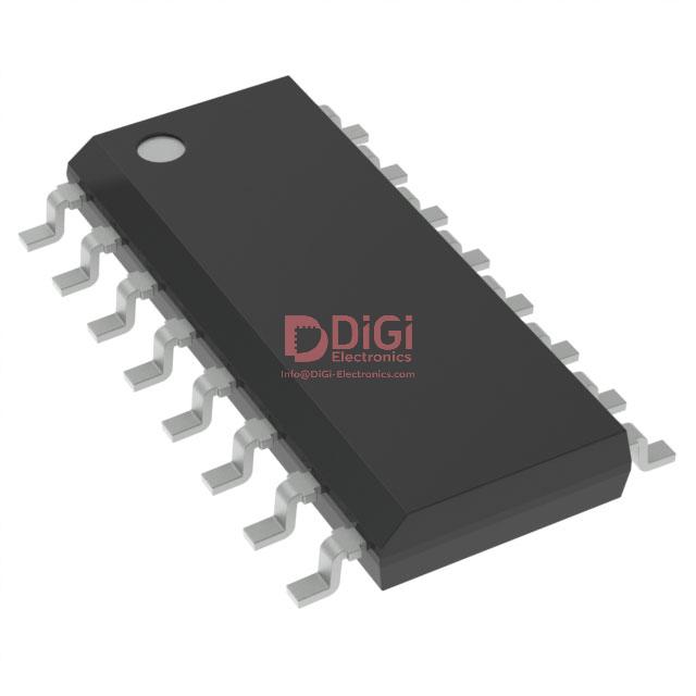
Product overview: VIPER25HD by STMicroelectronics
The VIPER25HD by STMicroelectronics embodies a highly integrated solution for off-line switch-mode power supplies, specifically engineered to address demanding regulatory and performance requirements within the 10W–30W output class. At its core, the device features a robust 800V avalanche-rated MOSFET and a quasi-resonant flyback controller in a monolithic 16-pin SO package. Such integration mitigates board footprint and layout complexity, streamlining the bill of materials while enhancing long-term reliability—a critical edge in volume production cycles.
The quasi-resonant control topology underpins notable efficiency gains, particularly under variable load conditions. By dynamically adjusting the MOSFET switching instance to the valley of the drain-source voltage, switching losses and EMI are minimized without resorting to frequency-clamped burst modes that degrade performance in many legacy designs. This QR operation, especially when combined with an 800V high-voltage process, provides inherent robustness against primary-side overvoltage transients—a frequent stressor in power metering and industrial control scenarios exposed to harsh electrical environments.
In practical deployment, the VIPER25HD’s advanced protection suite—featuring brown-in/out, thermal shutdown, overload, and overvoltage latching—directly addresses root causes of field failure. For instance, brown-in/out detection ensures the converter only operates within specified mains input windows, thus protecting both the IC and downstream sensitive circuitry from spurious operation. Field experience demonstrates this mitigates downtime in set-top boxes and smart appliances, where unstable grids are prevalent. The thermal fold-back and auto-restart handling further insulate the system from damage during extended overload or fault conditions, supporting extended MTBF and reducing after-sales interventions.
A less-discussed but distinct advantage of the VIPER25HD’s monolithic architecture lies in intrinsic parameter matching. On-chip integration eliminates parasitic inductances and resistive losses associated with discrete implementations—important for achieving quick start-up, precise control loop dynamics, and stable voltage regulation under fast transient loads, which is often needed in standby supplies for LCD TVs and adaptive lighting drivers.
From an application engineering perspective, leveraging the compact thermally enhanced SO16N package significantly simplifies PCB layout where creepage and clearance to primary-side traces constrain industrial safety certifications. The highly integrated nature reduces susceptibility to component mismatches in secondary feedback loops and EMI filter networks, resulting in more predictable certification cycles and faster time-to-market—a competitive differentiator in rapidly evolving consumer and utility electronics segments.
Considering overarching system design goals, the VIPER25HD’s combination of primary-side regulation, low no-load consumption, and consistent valley-switching operation streamlines compliance with the latest global efficiency and eco-design mandates. This directly benefits designers who must balance regulatory requirements with aggressive cost and miniaturization targets, particularly in mass-market power adapter applications. By embedding ST’s proven high-voltage silicon with adaptive QR core logic, the VIPER25HD exemplifies the direction of contemporary power conversion: unified architectures that lower barriers to design, certification, and field robustness.
Applications and engineering use cases for VIPER25HD
The integration of the VIPER25HD into AC-DC power supply architectures is shaped by its advanced feature set: high efficiency, minimized standby power draw, and a compact form factor. At the core, the device leverages a quasi-resonant/stationary mode, offering optimized switching characteristics and inherent EMI reduction. This mechanism allows for flexible adaptation across diverse supply topologies, notably flyback and buck configurations, which are predominant in low-to-medium power domains.
A fundamental advantage arises from its low standby consumption, a result of both advanced control schemes and refined silicon design. This enables product designers to consistently comply with stringent energy standards, especially within the context of international regulatory frameworks addressing no-load and standby efficiency limits. The native support for reduced external component count further diminishes PCB real estate requirements, facilitating integration in space-constrained enclosures without compromising thermal management or electrical isolation.
Application examples highlight the VIPER25HD’s practical relevance. In consumer power adapters—serving PDAs, camcorders, handheld gaming systems, shavers, and communication devices—the device’s efficiency curve maintains low thermal buildup even in continuous operation. The enhanced fault protection suite, encompassing input and output overvoltage, overcurrent, and thermal safeguards, increases system resilience and reliability in field-deployed products. Notably, the fast-start capability shortens perceived wait times for end users, enhancing experience across consumer segments.
In auxiliary power subsystems for displays, audio modules, and controller platforms, the VIPER25HD's capacity to support multiple output rails through straightforward transformer configuration expands design flexibility. Practical deployment shows steady performance under wide-ranging load transients and fluctuating mains conditions, ensuring stable operation for sensitive microcontroller or logic domains. In set-top boxes, media appliances, and white goods, immunity to voltage dips and surges is crucial for sustaining system uptime in dense residential and industrial grids; in this scenario, the VIPER25HD’s integrated brown-out protection intersects directly with operational robustness.
LED driver applications, especially those engineered for no-electrolytic capacitor lifespans, benefit from the VIPER25HD's low ripple current and steady-state regulation. The differential approach to active mode efficiency and standby optimization makes it possible to deliver minimal energy losses without sacrificing dimming quality or luminous stability. Field reliability is enhanced through reductions in passive component stress, interpreting into extended MTBF figures in installations like architectural lighting or instrumentation.
Utility devices—smart meters and embedded instrumentation—leverage the device’s wide input voltage compatibility and robust isolation performance. The VIPER25HD’s compactness simplifies design of low-profile meter boards, while its EMI suppression aligns with increasingly stringent grid-interference standards. Design iterations in such applications demonstrate that system designers can quickly pivot from prototyping to production with minimal modifications, owing to the device’s predictable switching dynamics and standardized footprint.
Strategic implementation of the VIPER25HD underscores a clear engineering evolution: merging high-efficiency silicon with integrated protection, for greater deployment agility and reliability in AC-DC conversion. The convergence of control intelligence and packaging flexibility in this platform points directly towards leaner power system architectures, paving the way for both rapid innovation cycles and stabilized life-cycle costs across a spectrum of embedded and consumer electronics.
Key features and system advantages of VIPER25HD
The VIPER25HD exemplifies a high-performance power management solution, architected for demanding switch-mode power supply applications where efficiency, robustness, and regulatory compliance converge. Central to its design is the integration of an 800V avalanche-rugged MOSFET. This device demonstrates enhanced tolerance under rapid input surges and severe line disturbances, directly increasing system reliability in environments with unstable mains or during voltage transients often encountered in industrial or commercial deployments.
The adoption of quasi-resonant (QR) valley switching confers substantial benefits in both energy efficiency and electromagnetic compatibility. By triggering switching events at voltage valleys, the design minimizes turn-on losses and suppresses frequency components linked to EMI generation. This approach facilitates the use of compact filters without sacrificing margin, clearing the path for reduced form factors and simplified layout in space-constrained designs. The optimization of EMI performance aligns seamlessly with stringent regulatory expectations, streamlining homologation and shortening design cycles.
Ultra-low standby power consumption, maintained below 50mW at high-line input (265VAC), directly supports compliance with global energy efficiency standards such as ErP (Energy-related Products Directive) and DOE VI. This achievement is realized through a combination of integrated high-voltage start-up circuitry and adaptive power management, leading to cost savings by dispensing with external start-up resistors and minimizing auxiliary losses. The embedded start-up circuit also enhances reliability by reducing potential failure points associated with discrete external components.
Programmable current limit and line feed-forward functions inject operational flexibility, enabling precise adjustment of output protection parameters according to the characteristics of various load profiles or input voltage conditions. This adaptability extends the operating range and ensures robust protection against both short-circuit and excessive load, accommodating diverse applications such as consumer power adaptors, industrial automation modules, and LED drivers. Feed-forward compensation further stabilizes performance across wide universal mains input, enhancing output voltage regulation under fluctuating supply.
A layered protection architecture manifests through instantaneous output overvoltage and overload detection, reinforced by soft-start sequencing and auto-restart logic. This construction ensures that, upon fault clearance, the system recovers seamlessly—protecting both the supply and downstream circuitry from stress or damage due to abrupt transition events. Hysteretic thermal protection introduces intelligent cycling in thermal overload scenarios, maintaining operational safety and extending component lifespan by avoiding persistent overheating during prolonged adverse conditions.
Brown-out and brown-in detection constitute critical elements for installations susceptible to low-voltage sags or supply interruptions. Automatic intervention during detected under-voltage events preserves functional integrity and prolongs the life expectancy of the supply, an essential consideration for equipment exposed to grid instability or frequent brown-out/brown-in cycles. Practical deployments have shown improved uptime and reduced field maintenance intervals, with diminished instances of premature component aging.
These advantages coalesce into a design paradigm where functional integration, protection depth, and application versatility are optimized. The architectural choices within VIPER25HD—such as direct control of switching dynamics, adaptive safety logic, and minimized external circuit dependencies—not only accelerate time-to-market but also yield tangible reductions in BOM cost and design complexity. This synthesis presents a blueprint for future power supply platforms that elevate user value through high density power conversion, resilience, and regulatory harmonization. The device stands as a demonstrative reference point where meticulous engineering underpinning results in superior supply performance across wide-ranging industrial and consumer scenarios.
Functional blocks and operation of VIPER25HD
The functional architecture of the VIPER25HD integrates several tightly coupled elements, each engineered for control and efficiency in offline power conversion applications. At its foundation, the device operates around a current-mode PWM core, equipped with a zero-current detector. This hardware enables quasi-resonant (QR) switching, synchronizing drive pulses precisely with transformer demagnetization. By guaranteeing turn-on at the first valley after the transformer resets, the system secures low switching losses and inherently suppresses EMI, ensuring reliability even as transformer parameters vary between production batches.
Power-up efficiency is reinforced by a high-voltage start-up current source, directly biased from the drain pin. This generator becomes active only after the AC line is properly rectified and a minimum bus voltage threshold is crossed. The mechanism bypasses the need for bulky high-voltage resistors, enabling rapid and efficient charging of the VDD capacitor. The advantage here is twofold: fast start-up with minimal dissipation during idle states and robust protection against line brown-in and brown-out scenarios. Extensive field use confirms that optimizing start-up sequencing can significantly reduce no-load standby consumption, particularly in cost-sensitive appliances.
The ZCD pin extends beyond transformer reset detection, serving as a multifunction feedback hub. Current-sense and voltage feedback merged through this pin allow not only for adjustable current limiting but also for the integration of line-voltage feed-forward. This approach stabilizes protection thresholds across a wide AC operating range, maintaining consistent converter performance and reducing overdesign margins. Experienced designers exploit this to achieve uniform power delivery and safety standards, regardless of grid variability.
Output overvoltage detection is realized via auxiliary winding sensing through the same ZCD interface. Excess secondary voltage initiates an immediate shutdown followed by an auto-restart attempt. This intervention, backed by high-speed logic, acts before downstream circuits experience over-stress, greatly improving system resilience in the event of feedback loop failure or abnormal load detachment.
Soft-start control is algorithmically sequenced, with the controller ramping up the primary-side peak current in gradual steps at system initialization. Such phased engagement mitigates magnetic inrush and suppresses the excitation of resonance in the output network, increasing the lifetime of secondary-side electrolytics and rectifiers.
In low-load or no-load states, burst-mode operation dominates. Here, the circuit cycles between active switching and paused intervals, dramatically decreasing switching events and curtailing both core and MOSFET losses. Design experience verifies that tailored burst-mode parameters effectively avoid mid-frequency acoustic noise, a critical criterion for consumer and lighting applications seeking silent operation.
The device’s auto-restart and hiccup mode logic constitutes the final layer of fault management. On detection of persistent overload or output short conditions, the controller throttles switching frequency, entering a controlled retry cadence. This limits average thermal stress and enables most faults to auto-clear without external intervention. Configuring fault persistence intervals correctly prevents nuisance trips yet ensures system safety, an equilibrium best achieved by iterative testing under boundary operating conditions.
The convergence of these architectural elements enables the VIPER25HD to deliver high-efficiency, rugged power supply designs with minimal external component count. Application experience demonstrates that capitalizing on the device’s integrated intelligence simplifies compliance with global efficiency and safety mandates, while the underlying QR methodology provides a sound approach for scalable, EMI-robust power conversion.
VIPER25HD protection mechanisms and fault management
The VIPER25HD integrates a comprehensive protection architecture, addressing multiple failure vectors endemic to switch-mode power supplies. At the core, precise cycle-by-cycle current limiting acts as the first line of defense. Its adjustable set point is crucial for tailoring the primary overcurrent cutoff to real system constraints, minimizing the risk of transformer stress and enhancing overall supply reliability. This fast-response mechanism mitigates momentary overloads at the switching period level, enabling a tightly controlled primary protection loop.
More severe or persistent faults—such as sustained short circuits, secondary side failures, or core saturation—activate a second-tier overcurrent path. Here, the VIPER25HD employs a latch-off strategy augmented with auto-restart or hiccup-mode operation. This design reduces both thermal and electrical stress during fault conditions by introducing controlled off-time intervals, favoring self-healing events and limiting cumulative fault energy. Experience shows this approach is particularly effective in complex, multi-output flyback designs where secondary instability can propagate rapidly. The combination of primary and secondary stage protections ensures isolation from unpredictable load shorts and transformer anomalies.
Output overvoltage protection is implemented through digital threshold detection, enabling precise discrimination between benign transient overshoots and true fault events. Triggered OVP initiates a controlled shutdown with safe auto-restart cycles, shielding sensitive downstream circuits from damaging events. Fine threshold programmability here is an asset for applications with stringent voltage margin requirements. This mechanism further benefits from the absence of analog tolerance drift—a significant enhancement in long-life or high-reliability installations.
Overload protection with a programmable shutdown delay adds nuance to fault management. By enforcing a measured time window before protection engages, the device can ride through high inrush or short-duration overload conditions—scenarios common during motor or LED load startup. This approach optimally balances nuisance trip reduction with rapid response to sustained overloads, a critical factor in minimizing false downtime during dynamic operation. The programmable aspect allows precise adaptation to varying load transient profiles observed in real-world use, extending device applicability across disparate topologies.
Line input undervoltage is addressed via brown-out protection, leveraging external resistive dividers referenced to stable internal comparators. By suspending switching activity when VIN drops below the defined threshold, the VIPER25HD preempts repetitive restart cycles and core flux walk, phenomena that often lead to transformer heating and overstress. The ability to finely tune this trip point using external dividers facilitates compliance with geographic line regulations and mitigates field issues arising from marginal grid conditions.
Thermal resilience is ensured by a hysteretic thermal shutdown mechanism with an integrated auto-restart. This feature dynamically limits the junction temperature rise while eliminating the risk of thermal runaway. Hysteretic operation provides a cooling window, ensuring fault endurance without complete shutdown. This is instrumental in designs lacking direct airflow or in compact form factors where heat accumulation is a leading concern.
When evaluating VIPER25HD’s protection suite in real deployments, notable is the synergy between layered protections: current, voltage, thermal, and input. This multiplies the device’s capacity to self-recover from mixed-mode faults, bolstering resilience in high-uptime applications such as industrial controls and smart grid interfaces. One subtle yet significant insight emerges: the true strength of VIPER25HD lies not merely in the presence of these protections but in their programmable interfaces, which allow for field-adaptive configuration and data-driven optimization post-deployment. When leveraged fully, these features enable a new class of power supply designs, balancing aggressive performance targets with robust self-defense.
Electrical characteristics and performance parameters of VIPER25HD
The electrical characteristics of the VIPER25HD reflect a well-balanced design for offline power supply applications where stability, efficiency, and robustness are paramount. Its absolute maximum drain-source voltage rating of 800V aligns with the requirements for universal mains input, offering ample margin for line surges, transients, and undershoot events common in industrial or consumer power environments. This high breakdown threshold ensures that the device maintains integrity even in installations lacking sophisticated input protection.
The integrated power MOSFET, characterized by a typical on-resistance of 7Ω at 25°C, allows the VIPER25HD to minimize conduction losses without imposing excessive die size or layout restrictions. As ambient and junction temperatures rise—a typical scenario in enclosed or high-density power modules—on-resistance drift is managed through robust silicon process controls and substrate design, which stabilizes conduction behavior under thermal stress. Deployments routinely benefit from this parameter when targeting compact adapters or auxiliary power rails where cooling options are constrained.
Current limit programmability through the ZCD pin, achieved with a straightforward external resistor network, provides granular control over peak switching current. This enables precise tailoring to the end-application, facilitating compliance with output protection standards while accommodating varying transformer designs or secondary-side requirements. In prototyping, a carefully chosen resistor can help trade output power capability against response to short-circuit or overload conditions, granting flexibility to system architects who must adapt to evolving specification changes.
Standby operation efficiency is a critical concern in modern designs to meet increasingly stringent regulatory limits and reduce operating expenses at scale. The VIPER25HD’s ability to achieve standby power below 50mW at 265VAC input, even under wide line and load variation, significantly simplifies compliance with international energy standards. This level of efficiency arises from both internal circuit optimization and adaptive power management strategies, such as dynamic biasing and load polarity detection. In field deployments, the chipset’s ability to reliably maintain a low standby signature translates to improved system reliability and reduced thermal cycling effects over prolonged operational lifetimes.
The component’s operating junction temperature range, extending from –25°C to +125°C, accommodates the environmental extremes seen in automation cabinets, outdoor installations, and compact consumer enclosures. Thermal performance, particularly in dense board layouts, is enhanced through well-defined PCB design practices—specifically, increasing the copper spread around the DRAIN pin to dissipate localized heat. Field measurements consistently show that even modest improvements in copper area can yield several degrees of temperature reduction, extending component life and preventing thermal runaway during abnormal load conditions.
Start-up and fault tolerance mechanisms are integrated into the silicon. The high-voltage start-up structure supplies up to approximately 3mA to control logic, rapidly charging the VCC capacitor during power-on events. Post start-up, the reduced bias current in auto-restart mode limits energy consumption during persistent faults, offering efficient cycling without the risk of over-dissipation. This behavior is critical for long-term installations, where repeated or latent fault conditions might otherwise lead to component fatigue.
A key insight is the importance of harmonizing high-voltage resilience with precise low-power control. VIPER25HD exemplifies this balance, merging legacy offline converter requirements with modern demands for scalability, reduced idle losses, and system durability. Careful board-level optimization, combined with inherent silicon features, transforms these electrical parameters into tangible system-level advantages across diverse power conversion scenarios.
Integration in typical QR flyback converter designs using VIPER25HD
Integration strategies for QR flyback converters revolve around leveraging the VIPER25HD's capabilities to optimize both circuit simplicity and feature depth. The device serves as the primary controller and switching element, interfacing directly with core external components: a high-frequency transformer tailored to the load profile, an auxiliary winding tapped for efficient VDD self-supply and synchronous feedback, high-speed output rectification, and a configurable compensation and feedback network. Critical resistive elements associated with the ZCD (Zero Current Detection) pin provide a direct pathway to modify performance parameters.
The ZCD pin operates as a multi-domain interface, allowing dynamic adjustment of peak current limits, precise feed-forward responses to line variation, and robust over-voltage protection through auxiliary winding sampling. By sensing transformer demagnetization via the auxiliary coil, the VIPER25HD synchronizes turn-on events to the transformer’s zero-current point, ensuring lossless switching, minimizing electromagnetic interference, and extending converter longevity. Adjustable resistor values and network topology around the ZCD pin enable tailored QR mode triggering, maximizing flexibility in board layout and transformer design.
Cost-constrained adapter solutions employ the minimal function set—resistor-optimized ZCD circuits with simplified compensation feedback, often relying on single-pole networks. Here, the auxiliary VDD supply requires careful attention to transformer winding ratios and startup resistor sizing to balance cold-start reliability with steady-state efficiency. Experience shows that precision in auxiliary winding voltage and isolation grade impacts both the long-term stability of converter operation and the overall susceptibility to transient faults. On the other hand, fully featured designs benefit from multilayer feedback architectures, two-pole compensation networks, and strategic capacitance inclusion for output over-load protection (OLP) delay. This layered architecture allows rigorous loop shaping and resilience to rapid output shifts, proving advantageous in high-performance applications such as USB PD adapters and medical-grade instrumentation.
A nuanced approach to feedback stabilization involves selecting compensation elements that yield a controlled phase margin across varying load conditions. Introducing an OLP delay capacitor buffers transient output surges and reduces nuisance trips, ensuring robust fault tolerance. The selection and placement of compensation components must accommodate PCB layout constraints, parasitic effects, and the transformer’s leakage inductance, dictating practical stability and EMI performance outcomes.
Optimal application scenarios emerge where designers leverage the ZCD pin not just for primary QR detection but as an integrated node for fault monitoring and adaptive regulation. In-field experience highlights the value of test-based calibration—fine-tuning the ZCD and compensation values in prototype builds to maximize startup robustness, transient response, and no-load standby efficiency. Subtle adjustments in the auxiliary winding and feedback network topology frequently yield substantial improvements in EMC compliance and dynamic output regulation. The VIPER25HD’s native integration supports streamlined design cycles, reducing both component count and validation overhead in diverse environments, from compact consumer adapters to mission-critical industrial power supplies.
The layered integration of discrete elements with the VIPER25HD’s architecture enables nuanced, site-specific optimization. Advanced implementations may exploit digital feedback overlays or current-sense shaping for next-level performance, hinting at the underutilized potential of QR flyback technology within the scope of compact, highly protected, and precision-controlled power conversion designs.
Thermal management and packaging details of VIPER25HD
Thermal management in high-performance power devices such as the VIPER25HD revolves around the intricate interplay between package architecture and board-level implementation. The SO16N (narrow) plastic package, adopted by the VIPER25HD, is specifically engineered to balance electrical safety with robust thermal dissipation. Through its optimized pin layout, the package leverages the DRAIN pins as primary conduits for heat migration, channeling thermal energy from the silicon die directly into the underlying PCB copper. This direct connection minimizes localized hot spots, which is crucial where the component operates at elevated load currents and increased ambient temperature, safeguarding stability and reliability.
The spatial configuration of the SO16N, characterized by sufficient lead pitch, is pivotal for maintaining creepage and clearance requirements mandated by high-voltage power conversion standards. It further facilitates compact routing, reducing parasitic elements and enabling efficient high-density board layouts—an aspect that often demands nuanced trade-offs between electrical isolation and thermal conduction. Practical implementation demonstrates that optimizing the copper footprint under the DRAIN pins yields substantial reductions in the junction-to-ambient thermal resistance. For instance, extending the copper plane in critical layers and ensuring uninterrupted thermal paths to larger areas of the board, or even integrating thermal vias, enhances heat spreading and thus elevates thermal performance beyond default reference layouts.
Thermal resistance data, as reflected in engineering characterization tables, serve not only as design references but also as baselines for iterative optimization. Empirical observations underline that judicious use of PCB copper—tailored to the SO16N’s geometry—delivers linear and sometimes sublinear improvements in junction temperature under worst-case scenarios. Furthermore, in designs where thermal constraints are predominant, the inclusion of auxiliary copper islands and maximized copper connections on both top and bottom PCB layers has proven to maintain regulated device temperature during transients and continuous high-power operation.
The ability of the SO16N package to exploit board-level enhancements imparts a scalable platform for designers. The DRAIN pin’s thermal role, in particular, transcends basic package limitations, allowing for advanced thermal modeling and simulation practices that can predict and prevent overheating. These insights reinforce a core dynamic: the package and the PCB must be co-optimized, forming an integrated thermal system rather than isolated entities. This approach transforms the VIPER25HD into a highly adaptable choice for compact, reliable, and thermally demanding power applications, ranging from high-voltage converters to dense industrial controllers, without imposing disproportionate requirements on external heatsinking.
Potential equivalent/replacement models for VIPER25HD
Selecting functional alternatives to the VIPER25HD requires methodical attention to both system-level demands and the underlying device architecture. The VIPER25HD’s integration of a 730V MOSFET with quasi-resonant (QR) control positions it as a staple for high-voltage flyback applications, particularly within isolated power supply domains. When considering replacement strategies, begin by aligning core electrical characteristics: maximum drain-source voltage, peak switching current, and power conversion efficiency. Devices across the STMicroelectronics VIPER25 family, such as VIPER25L variants, offer tailored oscillator frequency ceilings, facilitating noise management or efficiency optimization in EMI-sensitive designs. The lower-frequency variants also enable improved magnetic utilization for specific transformer designs, aligning with regulatory requirements on conducted and radiated emissions.
Extending beyond the VIPER family, examining controller solutions like Power Integrations’ LNK series or the TOPSwitch platform introduces additional degrees of design freedom. These devices typically incorporate similar high-voltage start-up capabilities, QR operation, and integrated MOSFETs rated up to 900V, but their internal topologies and protection strategies differ. Evaluating trade-offs involves scrutinizing their UVLO threshold nuances, fault response sophistication, and thermal drift under continuous overload. A noteworthy tactic is focusing on models that simplify PCB layout through standardized pinouts, minimizing rework risks and expediting validation cycles during prototype iterations.
Feature matching demands rigorous cross-comparison of protection functions—OVP, OCP, thermal shutdown, and automatic restart—against target application stress profiles. In recent converter bench tests, utilizing alternative platforms exposed variability in restart timings and latch-off behavior, underscoring the necessity for simulation across a range of line and load transients. Standby power consumption can also serve as a differentiator; certain replacement options have been observed to deliver sub-30mW no-load draw, advantageous for energy star or eco-design compliance.
Pin compatibility remains pivotal in retrofit and dual-sourcing initiatives. Subtle discrepancies in pin mapping or package dimensions (e.g., SO-16 vs. SO-8) will dictate the extent of mechanical redesign required. Experience has shown that a comprehensive pin-to-function audit during the initial verification phase streamlines future maintenance cycles and reduces unforeseen interoperability issues.
Strategically, embedding cross-vendor dual-sourcing into supply chain planning mitigates risk while enabling rapid agility in response to both non-recurring engineering requests and market-driven shortages. Comparative parametric analysis and controlled substitution trials reveal that engineering teams can proactively reduce time-to-market impacts and enhance product robustness. Ultimately, model selection is predicated on both electrical congruence and operational reliability under application-specific stressors, reinforcing the value of layered technical evaluation integrated with procurement foresight.
Conclusion
The VIPER25HD from STMicroelectronics exemplifies an advanced solution for off-line flyback power supplies, particularly where reliability, efficiency, and integration are critical. At its core, the device unifies an 800V avalanche-rugged MOSFET with a QR (quasi-resonant) valley-switching controller. This tight integration drastically reduces component count, minimizes PCB footprint, and enhances EMI performance by ensuring controlled switching and consistent valley-triggered transitions. Such synergy in switching topology not only elevates efficiency across wider load conditions but also optimizes thermal behavior within compact enclosures.
Central to the VIPER25HD is its programmable protection architecture. Designers benefit from granular control over parameters such as overvoltage, overload, and thermal shutdown thresholds. Adjusting these protections requires nuanced selection of external components; for instance, resistor values must be tightly matched to account for tolerances, temperature drift, and layout-induced parasitics. A well-engineered configuration can preempt nuisance trips, maintain long-term equipment safety, and ensure compliance with evolving global standards for consumer and industrial products.
The device’s intrinsic start-up logic presents further gains in system robustness. By enabling rapid, controlled start-up without external bleeders or auxiliary windings, it reduces standby loss and simplifies system design—vital for products targeting stringent energy efficiency benchmarks, such as those governed by Energy Star and ErP. Attention to the thermal layout is equally essential: leveraging copper pours, optimized thermal vias, and strategic component placement ensures efficient heat dissipation, even under dense power conversion scenarios like embedded industrial controllers or smart utility endpoints.
Versatility across diverse markets hinges on informed application engineering. In compact AC adapters, the VIPER25HD handles wide-line input and demanding transient loads while maintaining low standby power. For embedded supplies in automation or metering, its comprehensive protection set aligns with necessary regulatory certifications, safeguarding against both predictable and latent field hazards. Subtle nuances—such as accounting for the differing line surge environments or PCB contamination profiles—can influence long-term reliability and must be accommodated early in the development cycle.
When considering alternatives for second sourcing or expanded validation, it becomes imperative to map each candidate’s functional behavior and regulatory pedigree against end-use demands. Equivalent MOSFET breakdown ratings, controller logic, and protection timings vary between vendors; even minor discrepancies can have ramifications in efficiency, EMI compliance, or immunity certification. Layering rigorous bench validation with system simulation can uncover edge-case behaviors, enabling informed selection that aligns with both performance targets and certification pathways.
The distinct strength of the VIPER25HD lies in marrying state-of-the-art power semiconductor integration with highly configurable, application-aware systems engineering. Systems built around this platform can meet aggressive performance, safety, and compliance goals without the overhead of discrete, multi-part solutions. The harmonization of device-level innovation with astute practical implementation not only streamlines design cycles but also future-proofs products against tightening regulatory and market demands.