 >
>


Introduction to VIPER28HD and Its Application Scope
The VIPER28HD is engineered to optimize design efficiency in high-voltage offline power conversion. At its core, integration of an 800 V avalanche-rugged power MOSFET with a current-mode PWM controller forms a unified device presenting advanced capabilities for auxiliary power supply architectures. Unlike conventional discrete assemblies, the monolithic approach simplifies layout, reduces external component count, and mitigates complex reliability concerns, directly addressing the needs of fast-paced design cycles in both consumer and industrial applications.
Internally, the device leverages robust switch-mode control with precise current sensing, ensuring rapid and stable response under variable line and load conditions. The controller’s native current-mode operation also facilitates inherent cycle-by-cycle protection, essential for safeguarding end equipment in unpredictable mains environments. The avalanche-rugged MOSFET permits handling of voltage transients—frequent in grid-connected appliances—minimizing failure risk and enhancing lifetime endurance critical in energy metering or home automation nodes.
From practical deployment, the wide input voltage window allows seamless adaptation to global mains standards, enhancing design reuse across geographical regions and regulatory requirements. Implementing the VIPER28HD in auxiliary power rails for smart home devices or embedded metering units demonstrates notable reductions in PCB area and thermal overhead, while integrated protection features—such as undervoltage lockout, short-circuit, and thermal shutdown—streamline certification and compliance workflows. The internal startup circuitry relieves designers from complex external networks, expediting prototyping and enabling faster iterations.
Designers benefit further from predictable EMI performance due to the controller’s frequency jitter and soft-start mechanisms, reducing downstream filtering challenges and improving pass rates on regulatory electromagnetic compatibility. The device’s efficiency optimization under light and heavy load cases aligns with contemporary eco-design directives, critical in products where standby consumption and operational cost are driver metrics.
A key insight is that deploying highly integrated switchers like VIPER28HD shifts the focus from low-level hardware troubleshooting to system-level power management and functionality enhancement. This abstraction accelerates the development of smart AC-DC adapters, IoT edge nodes, and advanced energy measurement hardware, fostering innovation by enabling compact yet robust design cycles. The inherent flexibility and protection envelope of the VIPER28HD empower optimization not just of isolated power rail performance, but of entire embedded architectures, opening pathways to enhanced capability and accelerated deployment in modern electronics environments.
Core Functional Architecture of VIPER28HD
The VIPER28HD exemplifies advanced power integration by embedding a high-voltage startup circuit, precision sensing FET, and low-jitter oscillator within a unified silicon substrate, optimizing both performance and reliability for offline, universal input applications. The backbone of its power stage is an 800 V, avalanche-rated N-channel MOSFET, engineered for resilience against voltage spikes common in input surges and line disturbances. This robust device architecture ensures sustained operation under harsh conditions, directly addressing the demands of industrial and high-reliability environments. The controller leverages a current-mode PWM approach, supporting real-time drain current monitoring through its integrated sense circuitry, and deploying cycle-by-cycle current limiting to tightly regulate output under dynamic loads, transients, and fault conditions.
Interaction between these functional blocks reduces the reliance on discrete components, drastically shrinking bill of materials and PCB footprint. The built-in high-voltage startup generator, directly fed via the DRAIN pin, facilitates initial charge of the VDD supply capacitor from the AC line, bypassing bulky external resistors and startup ICs. Once the controller transitions to steady-state, auxiliary-winding-driven VDD supply eliminates startup losses, seamlessly switching operational modes to maximize efficiency and reliability. These mechanisms streamline board-level design tasks such as layout, thermal management, and EMI mitigation, enabling denser and more cost-effective implementations without compromising regulatory compliance.
Deployment in isolated flyback topologies demonstrates substantial benefits. Integrated avalanche ruggedness and fast drain sensing yield repeatable current-limit behavior—even with wide-ranging input voltages—preempting overstress events that typically degrade magnetics and primary-side switching devices. The architecture’s inherent noise immunity, imparted by the oscillator and optimized signal paths, supports stable operation in environments with high conducted and radiated interference. This tight integration empowers designers to balance safety, EMI performance, and power density, particularly in systems requiring universal input and stringent efficiency targets, such as appliance adapters, industrial controls, and IoT edge devices.
Experience shows that leveraging the internal startup circuit not only reduces board complexity but also mitigates cold start failures and start-up timing variability, both key considerations in supply qualification for geographically distributed high-line installations. Efficient cycle-by-cycle current limiting facilitates predictable behavior during overloads, improving downstream fuse coordination and ensuring consistent protection regardless of input conditions. These insights underscore the value of the VIPER28HD’s functional architecture in advancing the reliability, manufacturability, and long-term stability of next-generation power supply designs.
Key Features and Technical Advantages of VIPER28HD
The VIPER28HD integrated switcher is engineered to address contemporary flyback converter requirements, combining advanced power processing mechanisms with robust input adaptability. At its core, the device integrates an 800 V avalanche-rated MOSFET, conferring substantial voltage headroom over the full envelope of global mains, from sub-100 V brownout events up to severe 265 V surges. This allows seamless deployment across diverse geographies and grid qualities without supplementary overvoltage protection elements, streamlining both schematic complexity and mechanical footprint.
Switching architecture selection is fulfilled via a dual-frequency operation mode. Designers can tailor system behavior by selecting either 60 kHz (L-type) or 115 kHz (H-type) fundamental switching frequency. Lower frequencies typically minimize switching losses and optimize efficiency in higher-wattage designs, while the elevated 115 kHz mode is advantageous for reducing magnetic component size and cost. These dual options facilitate the right balance across efficiency, transformer dimensions, and EMI mitigation, indispensable for iterative design cycles and late-stage optimizations.
To further curtail electromagnetic interference, VIPER28HD leverages internal frequency jittering. By modulating the clock within ±4 kHz (for 60 kHz operation) or ±8 kHz (at 115 kHz), the device disperses electromagnetic energy over a wider spectrum. This mechanism significantly diminishes spectral peaks in both conducted and radiated emissions, streamlining filter design and improving prospects for passing stringent EMI certification upon first submission. The embedded spread-spectrum approach eliminates reliance on external EMC solutions, conserving overall bill-of-materials and PCB area.
Power efficiency, both under load and in standby, is prioritized through a proprietary burst mode strategy. Under light or zero load, VIPER28HD enters a burst switching regime, yielding no-load consumption of as little as 30 mW at 230 Vac. This meets and often exceeds the threshold for most international efficiency and eco-design standards—including requirements for household and industrial devices persisting in standby mode. The natural consequence is a marked enhancement in end-system energy ratings and minimized thermal footprint, particularly valuable in IoT and always-on applications.
Flexible current management is realized via the CONT pin, supporting adjustable current limitation through a simple resistor configuration. This precision scaling ensures robust alignment with transformer characteristics, output stage requirements, or specialized protection profiles. Field deployment often reveals transformer tolerances or load transients that challenge standard limiting, yet the analog programmability here allows preemptive tuning for fault resilience and application-specific performance targets.
Through these layered enhancements, VIPER28HD aligns with real-world engineering workflows: minimizing iteration cycles due to EMC or efficiency shortcomings, simplifying regional productization, and maintaining compact designs without trading off regulatory headroom. The convergence of high-voltage robustness, EMI suppression at the silicon level, configurability, and ultra-low standby loss sets a template for power conversion topologies targeting tomorrow’s regulatory and operational landscapes.
Electrical Characteristics and Power Handling Capabilities of VIPER28HD
The VIPER28HD integrates an 800 V-rated MOSFET, delivering robust voltage withstand capabilities essential for operation in wide mains-voltage environments and exposure to line transients. The low R_DS(on) of 7 Ω at 25°C optimizes conduction losses without sacrificing switching performance, directly benefiting overall efficiency. This parameter is instrumental when designing for low standby consumption, as it influences both static and dynamic power losses during off-load and light-load conditions.
Power handling for the VIPER28HD is shaped by a synergy between semiconductor properties and external circuit constraints. Output power is inherently set by thermal limitations; efficient heat evacuation is critical to prevent MOSFET temperature rise beyond recommended limits. Open-frame designs leverage airflow and increased PCB copper on the DRAIN pad, while enclosed supplies demand precise heat-sink attachment and tailored thermal vias. Utilizing expansive copper pours beneath the DRAIN pins directly bolsters thermal conductivity and enables reliable operation at higher ambient temperatures. Practical deployment often involves iterative calibration of copper area versus thermal rise, correlating PCB layout experimentation with measured device temperatures under load. Derating techniques and thermal measurements during design validation help uncover optimal safe operating points, balancing size, cost, and output capability.
The internal high-voltage current source plays a pivotal role during system startup, biasing the VDD pin until the auxiliary supply assumes control. Correct sizing of the VDD capacitor (C_VDD) is not simply a matter of bulk capacitance; it must synchronize with startup current capability, system load at power-up, and timing tolerances under worst-case ambient and input conditions. Improper selection risks incomplete startup or excessive stress on the IC’s internal structures. Experienced designers frequently simulate and empirically adjust capacitance values—using programmable loads and variable input voltages—to guarantee reliable turn-on, eliminate hiccup modes, and provide adequate margin for slow supply rise times characteristic of high-inrush environments.
The device’s soft-start mechanism introduces a controlled increase in current limit, suppressing inrush currents and dampening voltage overshoot across the MOSFET and output rectifier. This progressive ramp not only safeguards power stage components but also influences electromagnetic compliance, as abrupt current surges often correlate with high di/dt noise events. Adjustments to the soft-start duration and current profile can aid in tailoring system compliance with EMI standards, while simultaneously prolonging component life by reducing thermal and electrical cycling. Successful applications often pair the VIPER28HD’s soft-start with downstream snubbing and layout practices, constructing a multi-layered approach to stress management and reliability enhancement.
A nuanced understanding of these foundational parameters—breakdown voltage, R_DS(on), power dissipation strategies, startup sequencing, and soft-start behavior—is pivotal. Careful engineering across each layer translates to power systems that combine compactness, ruggedness, and efficiency, aligning field performance with demanding safety and endurance benchmarks, particularly in industrial and consumer environments marked by wide line fluctuations and space constraints. The VIPER28HD’s integrated characteristics, when systematically exploited, yield a platform that efficiently bridges design flexibility with hardened power conversion, setting a distinct benchmark in auxiliary supply engineering.
Protections and Control Mechanisms in VIPER28HD
Protections and control mechanisms in the VIPER28HD are architected to deliver resilient power conversion under varying operational scenarios while reducing reliance on peripheral protection hardware. The approach evolves around a multi-layered integration of sensing, feedback, and fault response systems, each contributing distinct boundaries and recovery paths for electrical abnormality containment.
The dual-level overcurrent protection (OCP) scheme leverages two threshold points: the first, IDlim, is selectable by external configuration and acts as the primary limit against ordinary overload events, enabling rapid detection and containment before device integrity is compromised. The secondary threshold, IDMAX, is engineered to counteract deeper faults such as transformer saturation or secondary diode shorts. Surpassing this boundary forces the converter into a hiccup or auto-restart cycle—a deliberate design to dynamically deactivate switching and thereby minimize cumulative thermal stress and component aging. In bench validation, this multi-tiered current limiting facilitates compliance with IEC safety standards, particularly in applications prone to high inrush or intermittent load spikes.
Output overvoltage protection (OVP) couples real-time feedback through the CONT pin with a customized analog divider, and overlays a digital noise filter plus multi-cycle event validation. This grants strong immunity to line-transient noise, which is prevalent in single- or multi-phase grids. The adjustable divider ratio permits fine-grained output voltage supervision; for instance, in telecom brick designs, this flexibility allows tighter setpoints near battery cutoff thresholds. Field deployment has evidenced improved shutdown accuracy, reducing downstream component overstress during rare line surge scenarios.
Overload protection (OLP) relies on feedback-path analysis. The timing of shutdown and restart is tunable via loop compensation network selection—opting for either single or dual-capacitor networks modulates the transient response and restart latency. This yields tailored fault management, adapting the converter’s profile for either repetitive short loads (such as motor precharge events) or steady-state heavy loads. Practitioners routinely exploit this adjustability when tuning converters for specific end-equipment cycles, achieving optimized recovery behavior without altering upstream architecture.
The Extra Power Timer (EPT) grants a programmable tolerance window for transient inrush or start-up surges, ideal for loads with high capacitive or cold-start requirements. Engineering the timer’s profile enables the power supply to ride through short-duration overloads ― supporting brown-out recovery and motor start conditions while avoiding premature latch-off. This mechanism was particularly effective in drive control boards, where short surges are functional rather than alarm conditions.
Thermal shutdown with hysteresis incorporates a die temperature sensor with calibrated restart threshold, avoiding oscillatory on/off cycling and ensuring thermal equilibrium is reached before re-engagement. When subject to repeated high-load events in ambient-constrained enclosures, this function delivers robust self-recovery, preserving device operating life under adverse conditions.
Burst-mode operation at very light or zero load is orchestrated to minimize switching events and eliminate frequency-dependent losses. The peak current clamp inside burst pulses mitigates audible noise artifacts, a critical consideration in high-efficiency standby designs for consumer appliances. Measurement of standby consumption on reference boards frequently demonstrates sub-50 mW performance, outperforming regulatory targets with no additional control IC required.
Auto-restart cycles, triggered by any major protection event, are timed to provide a low-frequency reset interval. This uninterrupted recovery protocol eliminates the need for manual intervention or external watchdog resetting. In production testing, this attribute accelerates fault clearing and extends mean time to recovery, a central consideration in mission-critical and remote systems.
The sum of these mechanisms positions the VIPER28HD to not just fulfill, but surpass, international safety and energy directives with intrinsic design margin. The architecture invites deployment across wide-ranging topologies—from compact IoT nodes targeting ENERGY STAR compliance to industrial controllers demanding rigorous self-protection. Intrinsic configurability and layered fault logic are instrumental in engineering simplification, yielding a platform that minimizes bill-of-materials while ensuring predictable and context-aware system resilience. These features underline a design philosophy where the convergence of dynamic protection and adaptive fault management directly translates to greater field reliability and deployment flexibility.
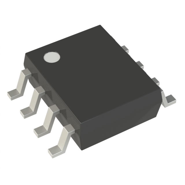
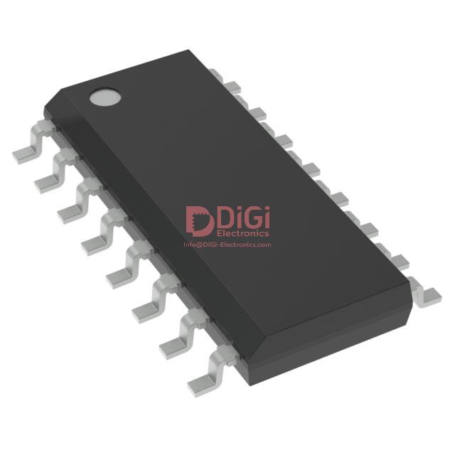
Package Options and Mechanical Considerations for VIPER28HD
Package selection directly influences both electrical performance and mechanical integration for the VIPER28HD switch-mode power IC. The 16-pin SO (SO16N) package, with its narrow body outline, is tailored for surface-mount workflows and compact PCB footprints. The pin arrangement facilitates efficient routing in high-density layouts, supporting automated assembly and enabling miniaturization. Close pin spacing demands careful signal integrity management, particularly in fast-switching, low-voltage applications prone to crosstalk or EMI. Leveraging strategic ground fills and guard traces between sensitive signal pins becomes critical as design margins tighten.
The DIP-7 package, conversely, addresses through-hole assembly and scenarios where mechanical robustness and creepage distances are essential, such as industrial or appliance power supplies. Its wider pin pitch sustains elevated surge isolation levels and is more forgiving during hand-soldering and rework cycles. This mechanical form factor tends to excel in environments where vibration or repeated mechanical stress is anticipated, notably in field-replaceable modules or ruggedized subassemblies.
Environmental compliance, achieved by ECOPACK® construction, assures reduced hazardous substance content, facilitating green manufacturing lines and simple downstream recycling. This design approach serves both regulatory imperatives and long-term sustainability goals, aligning with major industry eco-initiatives.
Thermal management presents a fundamental design constraint, with peak junction temperature directly tied to layout practices. For SO16N configurations, maximizing copper pour under the DRAIN pins and extending these areas to thermal vias is essential for dissipating switching loss heat. Empirical PCB prototyping shows that each incremental increase in the copper footprint below the DRAIN node can yield measurable reductions in device temperature at loaded conditions, supporting operation closer to the datasheet’s continuous output rating. In dense layouts, stacking multiple ground layers and connecting them with via arrays improves heat dispersion beyond the immediate component region.
Careful modeling of power dissipation, aided by simulation and iterative hardware validation, reveals that the practical safe operating area hinges upon not only steady-state thermal impedance, but also transient behavior during load surges. Real-world deployments often benefit from coupling thermal sensors to PCB hotspots and implementing airflow management in constrained enclosures.
Ultimately, package choice and accompanying mechanical decisions shape the functional envelope and field performance of the VIPER28HD. While SO16N offers flexibility and miniaturization, the DIP-7 prioritizes isolation and resilience. Effective thermal design, grounded in robust PCB layout and thoughtful system integration, remains indispensable for unlocking the device’s rated power capabilities and longevity in demanding application scenarios.
Potential Equivalent/Replacement Models for VIPER28HD
In evaluating potential equivalents or replacements for the VIPER28HD, it is essential to dissect device requirements into tightly defined electrical and application-specific parameters. The choice of substitute centers on essential metrics: breakdown voltage, the thermomechanical resilience of the integrated MOSFET, adjustable switching frequency capability, and the granularity of onboard protection features. Within the STMicroelectronics VIPer Plus lineage, options like the VIPER26, VIPER35, and VIPER16 present nuanced trade-offs. For example, the VIPER35 delivers higher output power margins, while the VIPER16 caters to ultra-compact designs with low standby consumption. These distinctions manifest concretely in converter topologies optimized for cost-sensitive consumer goods or industrial auxiliary rails, where package footprint, BOM minimization, and startup current become decisive.
Transitioning to cross-brand alternatives requires filtering by both electrical and systems integration criteria. High-voltage flyback controllers from vendors such as Power Integrations (e.g., TinySwitch or LinkSwitch series) and ON Semiconductor must be scrutinized for universal input compliance, startup management, and fault detection logic. Interoperability at the EMI/EMC level is especially critical: core transformer resets, di/dt control, and snubber integration often differ subtly, affecting conducted and radiated emissions profiles. In practice, design reroutes have exposed secondary impacts, such as the influence of gate charge characteristics on switching losses at elevated ambient temperatures or the interaction of burst-mode implementations with downstream voltage supervisor ICs.
Application fit extends beyond headline electrical compatibility. Standby power thresholds—critical for meeting global efficiency standards like DOE Level VI or EU CoC Tier 2—are directly influenced by controller quiescent draw and switching algorithm. Design experiments have shown that even nominally compatible substitutes may require recalibration of feedback loop compensation or adjustment of thermally conductive PCB areas to maintain junction temperature targets.
A systematic cross-check of pinout and package conventions cannot be overstated. Instances of PCB rework have uncovered subtle misalignments in NC, sense, or enable pin positioning that, if overlooked, compromise either functional safety or diagnostic telemetry. Even when datasheet metrics present parity, simulation and targeted bench validation under full load, brownout start, and fault injection scenarios are instrumental in preempting unanticipated stress or incompatibility. This disciplined qualification workflow anchors robust field deployments and derisked product launches, reinforcing the imperative to balance device-level equivalence with system-level integration for long-term reliability.
Conclusion
The VIPER28HD from STMicroelectronics is architected to streamline the design process for auxiliary and compact primary power supplies by integrating critical blocks within a single package. At its core, the 800 V MOSFET enables direct connection to wide input ranges, sharply reducing the need for upstream protection and voltage conditioning components. The adoption of current-mode control, implemented with precision internal circuitry, ensures stable regulation across varying load and input conditions while inherently providing fast response to transients. Layered onto this are protection mechanisms including overvoltage, overload, thermal shutdown, and advanced brown-out detection, each embedded to offload risk mitigation from the designer’s BOM and layout.
Frequency agility is another cornerstone of the VIPER28HD design. Programmable switching frequencies and an embedded jitter function allow for fine-tuning of EMI profiles, aiding in the rapid clearance of international regulatory benchmarks. In applications ranging from consumer appliances to industrial control systems, this translates to compliance with minimal filtering overhead. The device’s low standby consumption extends the operational margin in energy-sensitive environments, facilitating both energy code adherence and thermal management simplification.
Application deployment benefits from reduced external part counts and straightforward PCB routing enabled by integrated startup and bias circuitry. This simplification, coupled with robust fault-handling, cuts iterative redesign cycles and accelerates prototype-to-production transitions. When recalibrating legacy equipment or launching new platforms, the VIPER28HD’s built-in feature set minimizes platform risk, especially in multi-standard or multi-environment use cases.
Experience shows that tightly integrated, protection-rich switchers like the VIPER28HD yield measurable improvements in long-term reliability, particularly in markets where service intervals are long and replacement costs escalate rapidly. Strategic selection based on a system-wide understanding of requirements—balancing efficiency, protection depth, and EMI latitude—positions the device as a forward-compatible solution within evolving technical landscapes. The ability to achieve design targets with fewer compromises stems from the device's architecture as well as its operational predictability under real-world disturbances.
The VIPER28HD thus exemplifies how judicious integration and thoughtful control topologies converge to create power conversion solutions that are not only regulatory ready but materially advantageous across the workflow from design conception to field deployment. This approach advances power supply engineering by compressing complexity and elevating system robustness, influencing both immediate design results and the broader trajectory of reliable, scalable power architectures.