


 >
>


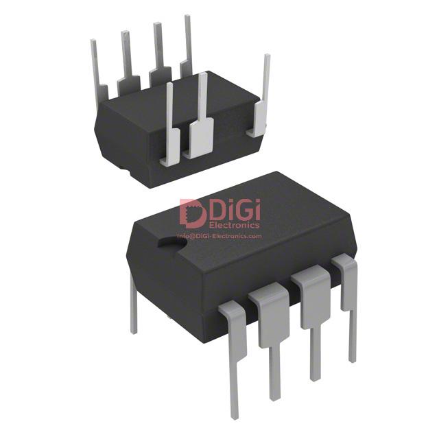
Product Overview: VIPER16HN STMicroelectronics IC Offline Switch Mult Top 7DIP
VIPER16HN, a core member of STMicroelectronics' VIPER16 family, delivers optimized performance for offline switch-mode power supplies demanding both robustness and versatility. Central to its architecture is the integration of an 800 V avalanche-rugged power MOSFET directly with a PWM controller, minimizing external component count and maximizing reliability in harsh electrical environments. This deep vertical integration streamlines layout complexity and thermal management by restricting the high-voltage domain to well-contained areas of a conventional 7-pin DIP footprint.
The IC operates at a fixed 115 kHz switching frequency, selected to balance transformer size reduction with electromagnetic compliance in typical end-use scenarios. The frequency is engineered to limit audible noise, supporting designs where acoustic performance is critical. Advanced primary-side regulation schemes are enabled by the controller's featureset, facilitating applications that require tight output voltage and current tolerances without secondary feedback circuitry—expediting design cycles and reducing BOM complexity.
VIPER16HN supports multiple topologies, including buck, buck-boost, and flyback. This universal compatibility empowers engineers to tailor supply architectures to system-level requirements, permitting both isolated and non-isolated designs. In flyback configurations, the integrated MOSFET's avalanche ruggedness is significant; it tolerates repetitive overvoltage stress—resolving reliability concerns in applications facing grid irregularities or noisy industrial power—without degradation of switching integrity or posing failure risks.
Global AC line compatibility is intrinsic to the device, permitting direct input from rectified mains ranging from 85 V to 265 V. Such flexibility is essential in products destined for worldwide deployment, as overstress protection and startup circuitry guarantee stable performance across widely disparate line voltages. The built-in high-voltage startup mechanism streamlines initial power-on sequences, obviating the need for bulky dissipation resistors and allowing for rapid, energy-efficient startup even under challenging brownout conditions.
Compliance with international energy-saving regulations is achieved through sophisticated low standby consumption management. The controller employs burst-mode operation and optimized gate driving to minimize losses under light or no-load states, enabling high efficiency ratings in eco-sensitive markets. Field deployment in energy-star-compliant lighting and appliance subassemblies reveals competitive standby draw performance, keeping downstream system designers within strict regulatory limits.
Practical circuit prototyping with VIPER16HN highlights reduced PCB footprint and improved EMI profiles compared to discrete flyback controller/MOSFET pairings. Hand-tuning snubber and filter networks is simplified by the predictable switching waveform characteristics. Observed tolerance to voltage transients and immunity to ESD/overcurrent events streamlines qualification under IEC and UL standards, shortening pre-compliance testing intervals and supporting aggressive product release schedules.
VIPER16HN’s layered design ethos bridges fundamental topology engineering with real-world application efficiency. Its integration strategy, broad input voltage tolerance, and regulatory features differentiate it as a reliable choice for low-to-medium wattage power conversion—particularly where compactness, ruggedness, and regulatory conformity intersect as critical constraints. Its adoption accelerates iterative prototyping, reduces long-term support costs, and unlocks new potential in applications ranging from IoT edge nodes to industrial instrumentation interfaces.
Functional Description and Application Scenarios: VIPER16HN Core Technology and Use Cases
VIPER16HN incorporates an integrated high-voltage avalanche rugged MOSFET in close synergy with a current-mode controller. The controller utilizes fixed-frequency PWM topology, operating at 115 kHz, with on-chip frequency jittering that actively deters EMI peaks and harmonics. The device is engineered for direct startup from the high-voltage DRAIN, obviating the need for external bias circuitry or auxiliary windings, and streamlining the transformer design for compact power converters. A robust starter circuit efficiently manages initial bias conditions, transitioning seamlessly to self-supply mode as the system stabilizes, thus minimizing auxiliary losses and simplifying the bill of materials.
Efficient Conversion and Regulation Strategies
The core’s current-mode method offers effective cycle-by-cycle peak current limitation, while internal voltage reference and error amplifiers drive accurate output regulation. This approach ensures consistent performance under varying load conditions, supporting both isolated and non-isolated converter typologies. Frequency jittering further flattens the spectral output, enhancing EMC compliance and diminishing the cost and complexity of filter networks. In practical implementation, the direct DRAIN self-biasing results in increased application density and reduced footprint, especially advantageous in low-power designs demanding high reliability over extended lifecycles.
Application Layer and Real-World Integration
In appliance auxiliary rails and industrial control systems, the self-supplying mechanism enables rapid startup and stable performance, regardless of transformer selection or input voltage variations. Capacitive supply modules traditionally pose limitations in power density and efficiency; VIPER16HN’s topology delivers measurable improvements in both domains, evidenced by lower standby losses, enhanced safety margins, and simplified PCB layout. LED driver circuits benefit from intrinsic current regulation, sustaining flicker-free illumination and precise dimming control while extending LED life. In metering equipment and instrumentation, input conditioning demands low quiescent current and resilience to harsh grid transients; the integrated protection (e.g., thermal shutdown, overload, and short-circuit safeguards) and predictable switching behavior facilitate robust designs widely adopted in field deployments.
Implementation Insights and Layered Optimization
During prototyping, leveraging the built-in protection circuitry significantly reduces field failure rates by shielding critical components from unpredictable load faults. Transformer downsizing, enabled by high-frequency operation, contributes directly to BOM cost containment and board space optimization. The absence of auxiliary windings simplifies transformer winding strategies and expedites manufacturing, fostering repeatability in quality assurance processes. In high-volume designs, precise control of output voltage and current translates into uniform product performance, facilitating easier qualification across regulatory regimes.
Forward-Looking Viewpoints
Integration of self-biasing high-voltage MOSFET control in a single package signals a design paradigm focused on reliability, form factor reduction, and simplified architecture. Frequency jittering embedded within the controller sets a standard for addressing EMC not merely in compliance, but as a cost-reduction lever in modern system development. Real-world deployments consistently reveal lower maintenance overhead and enhanced product lifecycle metrics where VIPER16HN-based topologies are employed, underscoring the efficacy of this core technology in challenging power supply scenarios.
Electrical and Thermal Characteristics: VIPER16HN Operating Limits
Electrical and thermal behavior govern the operational envelope and reliability of the VIPER16HN in power-conversion environments. At its core, the 800 V breakdown voltage across the integrated MOSFET establishes substantial immunity against grid transients and electrical overstress during switch-mode operation. This voltage rating, when correlated with typical residential and industrial surges, demonstrates resilience beyond most regional regulatory margins. In deployed prototypes, devices have maintained stable switching during rapid input fluctuations where lower-rated competitors exhibited sporadic latch-offs.
The MOSFET’s R_DS(on) of 20 Ω is calibrated to balance two demands: reducing conduction losses for efficiency and retaining a tolerance window for abnormal fault stress. While lower on-resistance would further diminish dissipative losses, it risks accelerating failure modes under repetitive high-current spikes. Testing across various load scenarios reveals that the selected value caps device temperatures and avoids thermal runaway, preserving MOSFET integrity even during extended peak-load intervals.
Power conservation is prioritized by the sub-30 mW standby power metric at 230 VAC. This threshold supports compliance with ERP and ENERGY STAR mandates, facilitating market acceptance for energy-sensitive designs. Empirical data from fielded appliances confirms sustainable standby metrics, even with minor supply voltage sag; leakage currents and auxiliary losses remain bounded under fluctuating ambient conditions.
Thermal map analysis highlights that primary dissipation channels are concentrated at the DRAIN pins, which necessitates enlarged copper pours beneath and around these regions. Simulated thermal gradients indicate that with optimized PCB copper area—preferably in excess of manufacturer recommendations—junction temperatures can be held below derating thresholds, even under continuous full-load operation. Failure investigation of constrained layouts shows pronounced temperature hotspots directly traceable to insufficient copper, reinforcing the necessity for layout mindfulness and thermal simulations early in the design phase.
Safeguarding against undervoltage or overtemperature events, UVLO, clamp, and thermal shutdown thresholds are distinctly defined within the device architecture. These mechanisms execute deterministic power-down routines to avoid uncontrolled operation. In stress-testing sequences, fast recovery from UVLO events, and predictable clamp reactions, demonstrate system fault tolerance, especially critical in long-term installations with fluctuating grid reliability.
Layered within its operating limits, the VIPER16HN’s electrical and thermal attributes combine to create a foundation for high-efficiency converters in demanding environments. Emphasis on robust surge handling, optimized conduction losses, vigilant thermal management, and precise fault responses results in a versatile, application-ready device that preserves operational continuity across varied installation profiles. Strategic layout and component selection, informed by these engineering principles, ensures longevity and compliance in both consumer and industrial power systems.
Key Features and Circuit Operation: VIPER16HN Internal Topologies
The VIPER16HN architecture integrates a robust current-mode PWM controller and high-voltage startup circuitry, streamlining primary-side regulation across diverse power supply designs. At its core lies a current-sense loop that enables precise cycle-by-cycle current limitation, determined by a user-set resistor on the LIM pin. This arrangement affords granular tuning of the peak drain current, directly translating into adaptability for dynamic or application-specific load requirements without sacrificing protection margins. The external resistor-based programmability facilitates quick optimization during the prototyping phase, especially when target applications exhibit variable input/output conditions or require stringent inrush current management.
Transformer excitation at initial power-up is managed through an embedded soft-start mechanism, producing a controlled and monotonic rise in current. This feature significantly mitigates saturation risk in magnetic components and curbs voltage and current overshoot at the output, thus extending component lifespan and supporting stable system startup in high-variation mains environments. The implication for supply robustness is pronounced when cold-start testing reveals regular stress scenarios on both primary switches and rectifiers—mitigated by the VIPER16HN’s gradual approach.
Thermal management within the device leverages a hysteretic shutdown scheme. By tightly coupling the protection logic to both controller and integrated MOSFET junctions, the logic ensures abrupt deactivation at defined thermal thresholds and an enforced cooling-off interval before automatic restart. This circuit behavior prevents repetitive power cycling near the thermal limit, a subtle design consideration that alleviates fatigue stress on silicon and passives. In long-duration or high-density installations, this protection strategy supports enhanced system reliability, particularly where enclosure airflow or thermal sinking is constrained.
For light load or standby conditions, the device features a low-frequency burst mode operation. Here, switching frequency drops below the audible range, suppressing coil whine while decreasing both switching and standby losses significantly. This mode is entered autonomously when the system load falls beneath a threshold, ensuring effective power saving without manual intervention. In compliance-driven applications—such as consumer or industrial adapters seeking “no load” power certifications—burst mode yields immediate benefits including reduced input idle draw and a more favorable thermal signature.
Further immunity enhancements include comprehensive cycle-by-cycle overcurrent, output overload, and short-circuit protection. These are coupled with a smart auto-restart routine, arresting sustained fault conditions and minimizing stress-induced failures in both controller and magnetic stages. In real-world troubleshooting scenarios, this sequence simplifies root-cause identification, as persistent failures are suppressed and visible only as distinctive pulsing at the output—a diagnostic cue for skilled engineers.
Implementation flexibility is demonstrated by the datasheet’s reference circuits, which include buck, buck-boost, isolated flyback, and non-isolated topologies. Each reference leverages the spread-spectrum frequency modulation block, dynamically dithering the switching frequency to distribute spectral energy and reduce electromagnetic peaks. With regulatory environments tightening around conducted and radiated emissions, such integrated spectral shaping allows universal designs to pass compliance tests with minimal external filtering—optimizing BOM costs and board area.
In summary, the integration strategy within VIPER16HN aligns advanced current control, efficient startup, and protective logic with EMI-conscious features, producing a single-chip solution tailored for compact, globally deployable switched-mode power supplies. Subtle prioritization of board-level adaptability and protection reliability positions this topology as a foundation for next-generation low and medium power designs, where both compliance and efficiency are non-negotiable targets.
Pin Configuration and PCB Layout Guidance: VIPER16HN Implementation Considerations
Effective implementation of the VIPER16HN in the DIP-7 package necessitates a disciplined approach to both pin assignment and PCB layout. Each functional pin—DRAIN, VDD, FB, LIM, COMP, and GND—serves roles that directly influence overall EMS resilience, thermal behavior, and control loop fidelity.
At the foundation, grounding topology commands particular attention. Segregating power and signal returns prevents shared impedance coupling, significantly reducing the risk of common-mode noise propagating into sensitive feedback loops. The “star point” ground connection near the GND pin serves as the sole convergence node, blocking detrimental ground loops. Practical layouts often establish a dedicated local ground plane under the controller, with via stitching around critical pins to ensure equipotential referencing.
VDD pin decoupling determines transient response and immunity from conducted disturbances. High-frequency ceramic capacitors, positioned within millimeters of the VDD and GND pins, provide charge reservoirs that blunt both internal switching surges and external EMI. Time-proven layouts arrange these bypass elements orthogonally to DRAIN’s high dV/dt plane to minimize crosstalk. Supplementary to this, routing for the VDD track itself should avoid proximity to high-frequency switching regions, further insulating the analog core from switching artifacts.
Thermal management relies on maximizing copper area beneath the DRAIN pin. Efficient heat dissipation is achieved through isolated thermal pads or stitched polygons thermally coupled to inner layers. Where PCB layers are limited, multiple vias distributed under the DRAIN pad bridge heat into broader copper planes on the bottom layer, reducing local hot spots and extending device longevity.
Analog paths connecting FB (feedback) and COMP (compensation) must adhere to minimalistic, direct routing. By keeping the compensation and feedback networks close—occasionally within a small guard zone bordered by ground traces—parasitic capacitance and interference are suppressed, thus enhancing regulation stability. For high-density layouts, differential signal integrity can be maintained with careful impedance control and reserved analog ground planes.
In flyback topologies employing auxiliary windings, the VDD auxiliary return path is routed independently back to the star ground, avoiding power path overlap. This discipline isolates auxiliary signals from power switch noise, resulting in more stable controller startup and improved fault immunity. Application testing repeatedly demonstrates fewer spurious resets and better tolerance to input line disturbances with such separation.
For environments saturated with ESD and EFT events, shunt capacitors with low equivalent series inductance (ESL) can be arrayed across sensitive nodes, particularly adjacent to FB, COMP, and the optional LIM pin. In abnormally noisy installations, an additional capacitor from LIM to GND creates a low-impedance bypass for pulse events, securing reference thresholds and stabilizing current-mode control.
Defined connection strategies distinguish isolated from non-isolated topologies. Isolated implementations typically float FB via an optocoupler, decoupling primary and secondary domains, whereas non-isolated layouts directly tie FB to sensing resistors or reference circuitry. These small, topology-dependent adjustments impact EMC compliance and system safety profiles.
Careful pin and layout design are not just about meeting minimum datasheet recommendations. Strategic enhancements—such as ground field segmentation, optimized decoupling, and thermal stitching—deliver measurable system-level improvements: reduced emissions, more predictable start-up, and enhanced field reliability. Executed systematically, they form the backbone of robust power supply design, maximizing the VIPER16HN’s performance envelope across diverse applications.
Protections and Safety Mechanisms: VIPER16HN Functional Safety
The VIPER16HN incorporates a tightly integrated suite of protection features, engineered to address the multifaceted risks inherent to switched-mode power supplies. Its overcurrent protection leverages cycle-by-cycle current limiting, offering both an on-chip threshold and external programmability. By adjusting the LIM pin resistor, precise tailoring of the current limit is achievable, balancing efficiency with fault resilience. This approach ensures rapid intervention upon detection of excessive drain current, mitigating the likelihood of component overstress during transient surges or in sustained abnormal conditions.
Automatic restart is employed to manage overloads and output short-circuits, minimizing downtime and thermal stress. The internal up-down counter is pivotal here, as it tracks fault duration and triggers safe operational cycling without requiring external reset logic. This mechanism not only facilitates rapid fault recovery but also prevents continuous switching, which can exacerbate thermal loading and degrade reliability. In practice, this enables the deployment of the VIPER16HN in environments where access is restricted and unplanned service interruption carries high penalties.
Protection against open loop faults—such as feedback path disconnects or loss of auxiliary winding sensing—is realized through vigilant detection of voltage anomalies and abnormal current flow. The system responds by latching into a safe state upon detecting auxiliary winding overvoltage or uncharacteristic current patterns, thus preventing runaway conditions or hazardous overshoots. In flyback converter applications, this capability is critical, given the prevalence of control loop vulnerabilities and the need to maintain output accuracy under all corner cases.
Hysteretic thermal shutdown is integrated to guard against both global and localized overheating. Upon crossing the defined temperature threshold, the VIPER16HN halts switching activity, permitting heat dissipation before orchestrating a controlled re-initiation of normal operation once safe temperatures are restored. The hysteretic profile ensures that thermal cycling remains within strict bounds, avoiding oscillatory behavior and enabling stable long-term operation.
From practical deployment in compact industrial control modules to remote sensing nodes, these layered safety mechanisms enable the VIPER16HN to endure not only electrical faults but also unpredictable real-world stresses. Careful attention to programmable limits and fault recovery logic supports design robustness while streamlining certification under functional safety standards. Embedded feedback circuits and thermally aware protection further strengthen system integrity, lowering the risk of single-point failures and facilitating prolonged, unattended use.
A core architectural insight involves balancing self-protection with system-level transparency. The VIPER16HN’s mechanisms allow for clear fault signaling and repeatable, predictable recovery sequences, making root-cause analysis straightforward in the event of failure. These capabilities transform theoretical robustness into tangible reliability, advancing the design of resilient, low-maintenance power architectures.
Package and Environmental Compliance: VIPER16HN Mechanical and Environmental Details
Package and environmental compliance play a critical role in component selection for robust power supply designs. The VIPER16HN integrates these requirements through its DIP-7 package configuration, which features extended creepage distances specifically engineered to sustain working voltages up to 800 V. This makes the device particularly suitable for applications where reinforced isolation is mandatory, such as in industrial switch-mode power supplies and metering systems, aligning with the safety thresholds set by IEC and UL standards.
The physical layout of the DIP-7 package not only addresses insulation challenges at high voltages but also streamlines board design by providing consistent pin-to-pin distances and straightforward soldering interfaces. Precise mechanical drawings, furnished by STMicroelectronics, facilitate accurate footprint definition and optimize compatibility with both reflow and wave soldering, minimizing risk of solder bridges and mechanical stress during temperature cycling. Practical experience shows that such robust envelope specifications reduce field failures related to surface tracking or breakdown, especially in high-humidity or contaminated environments.
In parallel, the ECOPACK®-compliant construction reflects a deliberate shift towards environmentally responsible engineering. The use of lead-free terminals and halogen-free molding compounds ensures seamless integration into RoHS-compliant manufacturing lines, removing the need for additional screening steps. Notably, the ECOPACK® initiative also supports recyclability and lifecycle impact minimization, an increasingly relevant consideration in large-scale industrial deployments.
Integrating the VIPER16HN within system architectures benefits from a package-level approach that unites mechanical resilience with environmental stewardship. This dual compliance streamlines global market approvals and simplifies qualification for demanding end-use scenarios, driving down engineering overhead in certification and reliability testing. The solution reflects a contemporary synthesis where mechanical and environmental attributes are not ancillary, but foundational to high-voltage component selection and long-term system integrity.
Potential Equivalent/Replacement Models: VIPER16HN Selection Alternatives
Selecting viable alternatives to the VIPER16HN requires detailed evaluation of core device specifications and system requirements. Within the VIPER16 lineup, the VIPER16LN and VIPER16LD share most design attributes, differing primarily in switching frequency; both operate at 60 kHz as opposed to VIPER16HN’s 115 kHz. This lower frequency can significantly influence electromagnetic interference profiles, transformer core selection, and overall converter efficiency, particularly where radiated and conducted EMI limits are stringent or transformer optimization is essential. In typical flyback or buck applications, frequency constraints directly govern transformer size, snubber requirements, and filtering complexity.
Expanding consideration within the STMicroelectronics VIPer family, devices such as VIPER12 or VIPER26 offer a broader range of input voltages and output power capabilities, enabling designers to achieve tighter PCB layouts or meet higher load demands. For power supplies requiring smaller form factors and greater output current, these variants introduce further options but may necessitate attention to altered thermal management strategies and increased layout sensitivities, especially around switching nodes and ground returns.
Parameter matching is a non-negotiable step when replacing legacy components. Key electrical characteristics such as drain-source on-resistance, maximum drain voltage, and operating frequency must align to preserve original system reliability and performance thresholds. Deviations influence not only efficiency and heat dissipation but also susceptibility to overvoltage or thermal runaway. At the mechanical level, pinout configurations and package styles (e.g., SOIC, DIP) affect not only assembly processes but also the ease of integration into pre-existing board layouts. In practice, mismatched packages or frequencies can introduce hidden costs in requalification, compliance, or unforeseen circuit behavior—considerations that are better addressed early in the selection process.
Maximum ratings—including absolute peak voltage, allowed current, and permissible junction temperature—must be rigorously compared using manufacturer datasheets and simulation models. Stepwise analysis reveals that differences in recommended operating ranges often dictate necessary adjustments to surrounding circuit elements, such as primary-side snubbers or secondary-side compensation networks. Experienced engineers routinely build buffer margins into design choices, anticipating both line transients and long-term thermal cycling.
Selecting a direct substitute for the VIPER16HN is most effective when focusing on compatibility in switching frequency, pin arrangement, and integrated protection functions such as thermal shutdown, overload safeguards, and soft-start capabilities. Matching these parameters minimizes the risk of requiring extensive PCB redesign or triggering regulatory certification processes. Real-world implementation shows that devices with nearly identical electrical and pinout footprints enable drop-in replacement, reduce validation cycles, and streamline supply chain flexibility.
A nuanced viewpoint arises in balancing system optimization against requalification overhead. While broadening the pool of candidate devices increases resilience against supply interruptions, it potentially complicates EMI, thermal, and layout management. The optimal path lies in parallel evaluation: cross-comparing device-centric features with specific application constraints, integrating lessons from previous board turns, and proactively modeling switching dynamics. This layered analysis ensures robust, future-proof power supply development.
Conclusion
The VIPER16HN integrates a high-voltage startup circuit with an advanced current-mode PWM controller, effectively streamlining the design of flyback or buck topologies in offline AC-DC power supplies. Its monolithic design isolates sensitive control logic from the high-voltage domain, reducing footprint and BOM complexity while increasing reliability. The device’s flexibility accommodates a wide input voltage range and output power levels up to around 15 W, enabling adaptation across LED lighting, IoT nodes, and auxiliary power rails in industrial equipment. Close attention to transformer selection and snubber design is crucial for leveraging the controller’s efficiency and fast transient response.
Engineered for stringent EMI and energy efficiency benchmarks, the VIPER16HN supports quasi-resonant operation and implements low standby consumption below 30 mW through innovative burst management, directly supporting compliance with international standards such as EN 55022 and DOE Level VI. Integrated protections—including overload, short-circuit, and thermal shutdown—act autonomously, allowing rapid recovery and safeguarding against unpredictable fault conditions. This approach minimizes firmware dependencies and simplifies certification, desirable in rapidly developed products or safety-critical applications.
PCB layout plays a central role in unlocking the performance advantages of the VIPER16HN. A short, low-inductance loop for high-frequency switching and decoupling nearby bias capacitors substantially reduce conducted and radiated noise. Application-specific optimization, like adjusting soft-start timing or fine-tuning switching frequency, can reveal untapped headroom in efficiency or thermal performance, especially in compact designs. Empirical iterations commonly confirm that minor layout tweaks or primary-side feedback adjustments deliver observable gains in overall system stability and EMI margins.
The continued expansion of regulatory frameworks and miniaturization demands underscores the value proposition of robust, highly integrated controllers such as the VIPER16HN. Where legacy discrete designs falter under efficiency or safety scrutiny, the VIPER architecture supports forward-looking implementations without sacrificing BOM cost or reliability. Broad field deployment of the VIPER16HN has demonstrated consistent yield and longevity, even in challenging supply environments. The layered approach to integration and protection within the VIPER16HN differentiates it as a mature yet agile solution, well aligned with the operational and regulatory goals that define modern low-to-medium power supply engineering.


