


 >
>


Product overview: VIPER17LDTR from STMicroelectronics
The VIPER17LDTR from STMicroelectronics exemplifies a compact, integrated solution for off-line flyback converter designs, addressing the tight efficiency, safety, and footprint requirements dominating low- to medium-power applications. Core to its functionality is an 800 V avalanche-rated N-channel MOSFET, monolithically combined with an advanced pulse-width modulation (PWM) controller. This level of integration eliminates the need for discrete high-voltage switching devices and external PWM drivers, directly shrinking component count and minimizing layout complexity. The 16-pin narrow SO package ensures PCB space remains minimally impacted while enabling straightforward thermal management.
At the silicon level, the device leverages high-voltage, high-reliability processes, translating MOSFET robustness into elevated surge tolerance and protection against line transients common in industrial and consumer environments. Avalanche-rated devices in this class reduce failure rates under single-fault conditions, a vital attribute for isolated power supplies operating from wide AC mains input. The controller section employs a fixed 60 kHz switching frequency, pre-tuned to reduce EMI emission around frequencies sensitive to regulatory class B standards. Integrated soft-start, overload and overtemperature protection, and brown-out detection further enhance operational resilience, pre-empting common failure and stress scenarios encountered during real-world deployment.
In practical flyback topologies, the VIPER17LDTR excels in high-voltage, low-power isolated auxiliary supplies, notably in appliance, metering, and building automation platforms. Its low standby consumption stems from an advanced burst-mode operation, maintaining regulation even at milliwatt levels while keeping switching losses and audible noise suppressed. In design iterations, leveraging the internal start-up cell accelerates power-on sequencing and removes the need for external high-voltage bootstrap components. The IC’s current-mode control architecture simplifies loop compensation and inherently tightens output voltage regulation across wide line and load excursions.
The systematic integration of protection features, such as output short-circuit, feedback disconnection, and thermal shutdown, address latent reliability gaps often revealed during field operation or compliance stress testing. Subtle design provisions—like low gate charge and fast recovery—also enhance switching efficiency and permit direct replacement in legacy circuits constrained by tight switching node dv/dt specifications. When measured against discrete implementations, the VIPER17LDTR yields quantifiable reductions in standby loss, complexity, and board area, directly translating into lower BOM cost and faster time-to-market.
A nuanced aspect is the device’s EMI performance under high dV/dt transients, which supports designs striving for ENERGY STAR compliance or similar eco-labeling, particularly in always-on or connected devices. Layout practices employing solid ground planes and minimized high-frequency loop areas further exploit the IC’s EMI strengths. For engineers, iterative bench validation with real-world AC sources typically reveals wide operating margin and a marked reduction in board hot spots, underscoring the synergy between the power stage and integrated controller.
The VIPER17LDTR’s architecture sets a benchmark for off-line switch-mode integration, future-proofing designs for evolving regulatory environments while affording flexibility, reliability, and manufacturability. Its orchestrated feature set facilitates rapid transition from concept to certified product, especially where design constraints and regulatory demands converge.
Key features and advantages of the VIPER17LDTR
The VIPER17LDTR serves as a highly integrated power management IC tailored for compact and reliable switched-mode power supplies. Central to its architecture is an embedded 800 V avalanche-rated MOSFET, which eliminates the need for discrete external high-voltage switching devices. This integration not only addresses space constraints on dense PCBs but also enhances device reliability under voltage surge conditions frequently encountered during line transients or inductive load switching. The ruggedness of the MOSFET allows power systems to endure challenging electromagnetic environments, reducing the likelihood of catastrophic failures and associated maintenance costs.
Pulse-width modulation (PWM) operation with frequency jittering is implemented to address the persistent challenge of electromagnetic interference. By dynamically modulating the switching frequency, the device disperses EMI energy across a wider spectrum, substantially lowering conducted and radiated peaks. This mechanism facilitates adherence to stringent EMI standards with cost-effective, simplified filtering schemes, serving both cost-sensitive consumer goods and industrial control systems that demand deterministic signal fidelity.
The incorporation of accurate, digitally programmable overvoltage protection (OVP) and configurable current-limiting circuits reflects an adaptable design philosophy. These features enable engineers to retrofit the VIPER17LDTR across diverse reference designs—ranging from low-power IoT adapters to auxiliary rails in industrial modules. The precise OVP implementation utilizes an internal voltage reference with tight tolerances, permitting predictable protection thresholds even under wide ambient temperature shifts, which is crucial for field robustness and regulatory compliance.
On-board soft-start management gently ramps up output voltage during power-up, preventing inrush currents that might otherwise stress rectifiers and filtering elements or trip upstream protection. Safe auto-restart routines intelligently diagnose and resolve transient faults—such as temporary overcurrent or overvoltage conditions—by periodically attempting recovery without manual intervention or system lockup. This closed-loop protection minimizes service disruptions, especially in applications like lighting control or smart appliances where continuous operation is imperative.
Thermal management is achieved through a combination of hysteresis thermal shutdown and burst-mode regulation. Upon excessive junction temperature, the device ceases switching activity and only resumes after adequate cooling, thereby averting silicon degradation or overload-induced drift. Concurrently, burst-mode at light loads reduces switching losses and maintains standby power below 30 mW at 265 VAC—aligning with evolving energy efficiency mandates for both consumer electronics and industrial controllers.
Input supply irregularities, such as voltage dips or brown-outs, are met by integrated brown-out detection that inhibits unsafe operation and prevents undervoltage latch-up. The dual-level overcurrent protection, spanning cycle-by-cycle limiting and hiccup mode, provides layered fault tolerance. In practical use, these features counteract the diverse fault profiles found in real-world installations—ranging from gradual overloads to abrupt short-circuits—with both proactive interruption and periodic auto-recovery.
Through the synergy of these mechanisms, the VIPER17LDTR positions itself as a cornerstone for designers seeking high-reliability, compact, and standards-compliant power conversion. The device's multidimensional protective schemes and adaptive control logic recommend it for emerging markets where long service intervals, rapid certification, and minimized total BOM cost are baseline requirements. Strategic use of the VIPER17LDTR, especially in systems with critical uptime needs or deployment in electrically hostile settings, enables solution scalability without sacrificing regulatory adherence or failure resilience.
Application scenarios and ideal use cases for the VIPER17LDTR
The VIPER17LDTR's high integration and configurability position it as a core component in diverse off-line AC-DC flyback converter solutions, where efficiency, reliability, and compactness are paramount. At its foundation, this device combines a high-voltage startup circuit, a PWM controller, and an 800V avalanche-rugged MOSFET. This consolidation allows direct connection to the rectified AC line, efficiently handling the wide input voltage fluctuations typical of global mains environments. The clamp-free snubberless topology further minimizes external circuitry, reducing losses and alleviating stress on both MOSFET and transformer, which are recurrent pain points in legacy designs.
Its versatility stands out in portable device adapters—PDAs, mobile phones, shavers, and gaming controllers—where integration reduces PCB size and streamlines enclosure constraints. The robust protection suite, encompassing thermal shutdown, overload, and overvoltage safeguards, enables compliance with demanding regulatory norms while minimizing field returns. The extremely low standby consumption (<30mW at 265VAC) is pivotal for charger applications mandated by global efficiency standards, eliminating the need for auxiliary standby circuits.
In consumer and industrial auxiliary power supplies—such as those found in display panels, monitors, set-top boxes, and white goods—the device’s quasi-resonant mode operation ensures low EMI and optimal efficiency across the load range. Notably, this operating mode also augments transformer life and lowers system heat generation, further contributing to long-term reliability. Design experience shows that leveraging the device's flexible feedback arrangement speeds up closed-loop tuning, enhancing overall system stability without iterative board spins.
For industrial and commercial LED drivers, the VIPER17LDTR’s capability to operate with minimal ripple current, and its support of no-electrolytic-capacitor (No el-cap) topologies, creates advantages in environments demanding heightened durability and maintenance cycles exceeding conventional consumer expectations. The elimination of large electrolytics translates to a reduction in both PCB area and potential wear-out mechanisms—a critical consideration for mission-critical signage or hard-to-access installations. This approach is reflected in field installations, where extended LED driver uptime is frequently linked to the avoidance of bulky, failure-prone capacitors.
Application in SMPS-based consumer devices such as computers and DVD players benefits from the device’s precise multi-mode control and fast line/load transient response, which jointly support robust operation even under brownout conditions or variable AC supplies. By integrating the start-up bias and driver circuitry, secondary-side complexity reduces, allowing engineering focus to shift toward fine-tuning EMC performance or optimizing thermal management.
A unique aspect in practical deployments involves system-level EMI compliance. The internal high-voltage start-up mechanism permits direct startup from high line, minimizing kickback that typically complicates EMI filter design. Experience underscores that, in dense multi-output topologies, careful grounding practices in combination with the VIPER17LDTR’s soft-start and frequency jitter functionalities suppress high-frequency noise, often negating the need for costly metal shielding.
In summary, the VIPER17LDTR enables power designers to converge mechanical, thermal, and electrical objectives within tight envelope constraints. Its feature set streamlines the development process, sets a high baseline for system reliability, and lowers long-term ownership costs, particularly for applications where longevity and regulatory compliance are not negotiable. The layered approach to integration and protection not only expedites time-to-market but also establishes the foundation for next-generation compact, efficient power platforms across consumer, industrial, and commercial domains.
Electrical characteristics and performance parameters of the VIPER17LDTR
The VIPER17LDTR integrates advanced silicon technology to accommodate input voltages up to 800 V BV_DSS, enhancing operational robustness in high-voltage environments while reducing external component count. Central to its performance is the embedded gate driver coupled with a proprietary SenseFET structure, enabling highly accurate and virtually lossless current sensing. This mechanism affords exceptional system protection and real-time current monitoring without the energy dissipation typical of sense resistors or legacy shunt techniques, a critical edge in designs subject to strict efficiency and thermal constraints.
Operating at a standard frequency of 60 kHz with a 4 kHz jitter range, the "L" variant prioritizes electromagnetic compatibility by spreading spectral energy, and supports efficient transformer utilization. In practice, frequency management balances conducted noise suppression against core losses, supporting the regulatory requirements of adapter and auxiliary supply designs. The device’s on-resistance, typically 20 Ω at 25°C, directly impacts conduction loss and thermal buildup. Field data indicate that this low R_DS(on) is central to achieving optimized power conversion in compact form factors, allowing for higher density layouts while maintaining temperature margins, particularly under derated airflow conditions.
Continuous output power rating is bifurcated by application topology—either enclosed adapter or open-frame configuration—with detailed derating curves available in the manufacturer’s datasheet. Engineers typically reference these charts to align maximum deliverable power with ambient temperature profiles, ensuring MOSFET junction temperatures remain within reliability thresholds over time. Subtle nuances such as enclosure design, copper trace geometry, and transformer selection further influence heat dissipation and ripple characteristics, often necessitating iterative thermal validation in prototype phases.
The integrated V_DD supply management features well-defined undervoltage lockout levels and internal soft-start sequencing. These address startup surge phenomena by gradually ramping gate drive, limiting peak current loads, and suppressing secondary diode reverse recovery stress. Empirical evaluation demonstrates that these timing controls result in smoother initialization, lesser transformer magnetics stress, and improved longevity of secondary-side components. In high turn-on surge scenarios, such as with large bulk capacitance or low impedance loads, this careful orchestration of supply thresholds proves essential in preventing voltage overshoot and minimizing RMS stress on output rectifiers and energy-storage elements.
From a system perspective, the VIPER17LDTR’s architectural integration of sensing, protection, and switching functions underlies its suitability for high-efficiency, tightly regulated AC-DC power stages. The device’s features permit designers to minimize peripheral verification while maximizing stability under dynamic load cycles. Integrated current sense mechanisms not only reduce bill-of-materials overhead, but also enable more agile fault response and system diagnostics in production deployments—an attribute that differentiates modern SMPS designs from traditional hard-switched topologies. Today, the VIPER17LDTR’s design approach demonstrates the progression toward intelligent power integration, where silicon-level precision and granular operational controls directly translate into significant system-level advantages in reliability, compactness, and design latitude.
Functional operation and protection mechanisms in the VIPER17LDTR
In the VIPER17LDTR, core operational strategies and protection systems are constructed to address the key demands of modern offline converters, especially where high efficiency and robust fault management are critical. At the heart of system initialization, a high-voltage startup circuit directly interfaces with mains AC, sourcing current to begin V_DD charging. This approach bypasses bulky passive components, optimizing layout and mitigating initial standby losses, until the transformer’s self-supply can take over. Integration of this function aligns closely with requirements for ultra-low standby dissipation and input surge robustness in industrial power supply architectures.
A precisely timed soft-start mechanism orchestrates a controlled ramp—in this device, an 8.5 ms trajectory. By gradually elevating output current from zero, component stress is distributed, protecting downstream rectifiers and the transformer core from inrush transients. This is practically significant in designs with tight thermal margins or sensitive magnetic components, where oscillations during startup can induce premature aging or erratic EMI behavior.
The current-mode PWM core is engineered for granular control and rapid protection response. Drain current monitoring on each switching cycle facilitates both cycle-by-cycle current limiting and immediate MOSFET gate disabling during overcurrent scenarios. Hardware configurability via the CONT pin and external RLIM supports field-level tuning, delivering a reliable path to balance transient response and safety cutoff thresholds. In applications requiring adaptive output power adjustment, such as dynamically loaded IoT gateways, this controllability proves vital to both reliability and system flexibility.
Overvoltage protection is realized through auxiliary winding feedback, augmented with the CONT input. The circuit actively surveils output excursion, transporting protection logic beyond traditional optocoupler bounds. Any significant voltage surges—often symptomatic of feedback network failures or control loop instability—trigger an immediate IC shutdown sequence, safeguarding both load and upstream supply domains. This relay avoids risky propagation of surge events, raising system resilience in compliance-heavy deployment scenarios.
Feedback and overload detection leverage advanced compensation and timing synthesis at the FB pin. Loop stability can be refined by varying the compensation network, with output overload detection programmed for optimal delay. By implementing a timed shutdown rather than instantaneous cutoff, the system achieves a compromise between temporary load transients and sustained fault conditions. This loop management is especially advantageous in multi-output flyback topologies, where slight fluctuations in auxiliary loads must not trigger repeated false shutdowns.
Burst-mode operation engages during extended periods of zero or low load, drastically curtailing average switching frequency. The result is substantial minimization of standby power—an imperative for energy-starved edge devices and compliance with international energy efficiency mandates. Smooth transitions in and out of burst mode directly influence quiescent noise floor and EMI signature, yielding tangible field performance improvements.
Brown-out protection is enacted via the BR pin, vigilantly tracking input voltage levels. With well-calibrated hysteresis, the system suspends switching when voltage sags beneath safe thresholds, impervious to transient noise spikes on the AC line. This function not only averts erratic power cycling but concurrently ensures operational conformity with grid-fault standards encountered in mission-critical and remote installations.
The architecture’s secondary OCP layer employs rapid-response hiccup mode for extreme fault cases—short circuits, core saturation, or persistent overload. Immediate gating of the power MOSFET interrupts fault propagation, while controlled autorun and restart pacing reduce cumulative thermal stress. This dual-level approach substantially enhances device survival under persistent stress, differentiating the VIPER17LDTR as a practical solution where fault isolation must coexist with uninterrupted system uptime.
Taken together, these deeply integrated functional blocks propel converter performance far beyond basic protection and control. Experience indicates that the interplay between soft-start smoothness, multi-tier current thresholding, and field-tunable feedback yields tangible improvements in reliability and compliance. A layered protection design that responds not only to instantaneous events but also to evolving operating conditions is essential for power supply engineers seeking both safety certification and operational longevity in complex power landscapes.
Package information and PCB considerations for the VIPER17LDTR
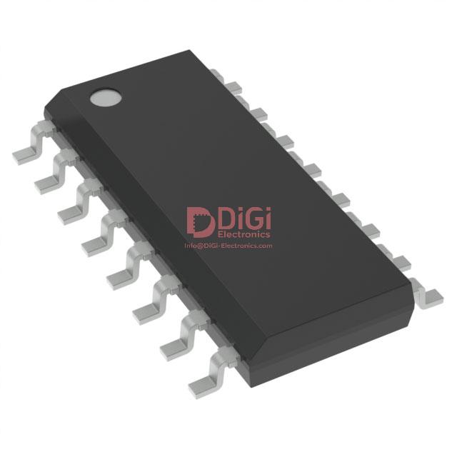
Package engineering for the VIPER17LDTR centers on the precision and practicality inherent in its SO16 narrow outline. This form factor streamlines automated pick-and-place, significantly reducing footprint constraints in dense electronic assemblies. The SO16 narrow body enables higher channel packing densities, supporting both single-layer and multilayer PCB architectures. Variants within the VIPER17 series, such as DIP-7 options, offer design flexibility for alternate assembly methods and thermal specifications, but the SO16 narrow variant remains optimal for compact, high-throughput environments where assembly speed and space savings are paramount.
Thermal management ranks as a primary concern during layout. The copper area directly beneath and surrounding the DRAIN pins must be methodically calculated to promote heat spreading and minimize junction temperature rise. Empirical data suggests that maximizing copper pours, coupled with via stitching in multilayer configurations, substantially reduces thermal impedance. In high-power prototypes, a minimum of 15 mm² copper connected to the DRAIN node demonstrably lowers chip operating temperature, with further gains achieved as copper area increases. Finite element thermal simulation remains a valuable tool for validating design in early development stages, ensuring reliable component longevity in production.
Compliance with ECOPACK® environmental directives is integral to VIPER17LDTR's qualification process. By adhering to RoHS and Pb-free standards, the device enables manufacturers to meet stringent regulatory requirements without additional process modifications, greatly simplifying supply chain logistics. The package utilizes lead-free plating and materials vetted for low toxicity and recyclability, contributing to overall lifecycle sustainability—a critical factor frequently assessed during risk analysis in new product introductions.
Isolation design demands rigorous adherence to creepage and clearance norms. The SO16 package offers sufficient pad-to-pad distances to support robust primary-secondary isolation, with PCB layout shaping these parameters through strategic routing and barrier placement. In practical high-voltage applications, designers frequently supplement layout with silkscreen markings and routed isolation slots, effectively elevating breakdown voltage ratings. Simulation and post-fabrication testing validate compliance with international safety mandates, ensuring that even under fault conditions, insulation barriers hold.
Maximizing performance in production deployments involves fine-tuning PCB layout across the power stage and feedback network. Minimizing the return loop area of high di/dt paths mitigates conducted and radiated EMI, often leveraging ground planes as shield layers to contain noise. Placement of snubber and filter components proximate to switching nodes further restricts transient propagation. Empirical validation through board-level EMI scans informs iterative improvements to trace width, ground referencing, and component orientation, culminating in a layout that achieves both thermal and electromagnetic integrity. In practice, attention to these details in early prototypes yields significant reductions in regulatory pre-compliance failures and lowers the long-term cost of design revisions.
A distinctive insight emerges when considering the interplay between package selection and layout discipline: engineering best practice dictates that thermal, EMI, and isolation demands never be siloed. They must be co-optimized from the block diagram phase onward. Leveraging the inherent versatility of the SO16 narrow package in conjunction with intelligent PCB strategies unlocks the full performance potential of the VIPER17LDTR for compact, safe, and environmentally resilient switch-mode power supply designs.
Potential equivalent/replacement models for VIPER17LDTR
In application scenarios involving flyback power conversion at moderate power levels, device selection extends beyond the VIPER17LDTR to encompass multiple optimized models within the STMicroelectronics VIPerPlus lineup. The VIPER16, VIPER27, and VIPER37, each present nuanced improvements or adaptations in terms of output power rating and available package variants. Incremental shifts in feature sets—from maximum drain-source voltage tolerance to embedded control logic—reflect tailored suitability for specific input voltages or protection requirements. In practice, the decision matrix expands as design constraints evolve: for high-frequency switching designs, higher maximum frequency ratings directly enable increased power density and reductions in transformer sizing, while enhanced integrated protection (e.g., brown-out, overtemperature, and overload safeguards) fortifies robustness and simplifies qualification cycles.
Comparative analysis of key functional attributes often reveals significant trade-offs. For example, the choice between a part with 800 V versus 730 V drain-source voltage margin can directly impact long-term reliability under transient conditions, particularly in environments with poorly regulated mains. Integrated soft-start, EMI optimization circuitry, or smart fault management further influences not only hardware design but also compliance with electromagnetic compatibility (EMC) standards and overall lifecycle cost. Leveraging internal experience with design iterations shows that applications demanding compact layout or minimal external overhead—such as USB, auxiliary supplies, or LED driver modules—benefit from higher integration levels and selectable frequency features. Conversely, in cases prioritizing thermal performance or wide voltage input, judicious selection across the VIPerPlus spectrum or comparable integrated controllers from other vendors affords measurable gains in efficiency and manufacturability.
Technical strategy for part substitution must also account for pin compatibility, thermal management, and switching behavior under diverse load conditions. Empirical validation on custom test boards frequently highlights subtle threshold differences across device generations, influencing startup profiles and fault recovery. Under typical engineering cycles, systematically evaluating these aspects—by matching electrical ratings, protection functions, and control topologies—enables direct migration without disrupting compliance or yield. This approach, underpinning progressive design methodologies, reinforces a trend toward highly integrated, intelligently protected offline switchers as foundational building blocks for modern power electronics architectures.
Conclusion
Evaluating the VIPER17LDTR within the landscape of off-line switching regulators requires an examination of its core architectural strengths and their implications for practical deployment. At its foundation, the device leverages a monolithic design, integrating a high-voltage startup circuit, an 800 V avalanche-rugged MOSFET, and advanced control logic. This level of integration streamlines the external BOM by removing the need for auxiliary startup components, current sense amplifiers, and external protections. The result is a reduction in both PCB footprint and component count, aligning with board space constraints encountered in dense adapter or auxiliary supply designs.
The VIPER17LDTR distinguishes itself with an advanced variable-frequency quasi-resonant operation, reducing switching losses and maximizing efficiency, especially under light load conditions. Its embedded burst mode ensures compliance with stringent modern standby and no-load power regulation requirements. This operational approach minimizes electromagnetic interference and simplifies EMI compliance, mitigating one of the persistent pain points in power supply certification.
From a protection standpoint, the device covers a comprehensive spectrum—featuring brown-out, overload, short-circuit, and over-temperature protections, all handled internally and with fast recovery. The automatic feedback loop compensation not only stabilizes regulation but also expedites design iterations, enabling rapid prototyping when developing for several form factors or input ranges. Real-world experience shows that such integrated fault handling accelerates time-to-market by limiting the necessity for custom shutdown or restart logic, which otherwise introduces unpredictable latencies and potential field failures.
Package selection and thermal design remain tightly linked to application-specific constraints. The SMD configuration of the VIPER17LDTR provides flexible mounting and improved thermal dissipation through PCB copper area optimizing, accommodating both high-density plug-in modules and low-profile embedded systems. However, careful validation of the MOSFET’s derating curve under peak-load, high-ambient scenarios is indispensable for sustaining reliability over extended operating life.
Application scenarios where the VIPER17LDTR demonstrates superior advantages include low to medium power adapters, industrial auxiliary power rails, and consumer standby supplies, particularly where regulatory compliance for standby power consumption is non-negotiable. Its robust protections enable operation in environments subject to input fluctuation and transient events without sacrificing long-term reliability. One noticeable insight is the device’s suitability for modular designs, where unified firmware and hardware platforms can leverage the same power stage with minor external adjustments, thereby streamlining supply chain and service considerations.
In summary, the VIPER17LDTR offers a nuanced balance of high-level integration, regulatory readiness, and comprehensive safeguarding features. A disciplined review of system requirements in the context of its built-in capabilities consistently reveals opportunities for reducing both cost and development cycles, positioning it as a compelling solution for next-generation high-reliability SMPS architectures.


