


Request Quote
(Ships tomorrow)
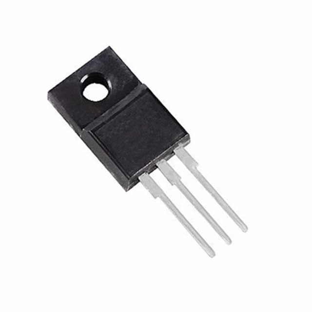
2SK4085LS N-Channel 500V 11A MOSFET Equivalent & Substitute Parts
Part Overview
The 2SK4085LS is an N-Channel MOSFET manufactured by onsemi, rated for 500V drain-to-source voltage with 11A continuous drain current at 25°C. The device is housed in a TO-220FI(LS) through-hole package and is designed for high-voltage switching applications. The product status is listed as Obsolete, making equivalent and substitute parts necessary for ongoing design support and procurement.
Substitute parts must maintain compatibility across critical electrical parameters including drain-to-source voltage rating, continuous drain current capability, gate charge characteristics, and through-hole mounting configuration. The following substitute devices have been qualified based on these parameters.
Substiute Parts
Key Parameters
| Parameter | Value | Unit |
|---|---|---|
| Drain to Source Voltage (Vdss) | 500 | V |
| Current - Continuous Drain (Id) @ 25°C | 11 | A (Tc) |
| Drive Voltage (Max Rds On) | 10 | V |
| Rds On (Max) @ Id, Vgs | 430 | mOhm @ 8A, 10V |
| Gate Charge (Qg) (Max) @ Vgs | 46.6 | nC @ 10V |
| Vgs (Max) | ±30 | V |
| Input Capacitance (Ciss) (Max) @ Vds | 1200 | pF @ 30V |
| Power Dissipation (Max) | 40 | W (Tc) |
| Operating Temperature (TJ) | 150 | °C |
| Mounting Type | Through Hole | — |
| Package / Case | TO-220-3 Full Pack | — |
| FET Type | N-Channel | — |
| Technology | MOSFET (Metal Oxide) | — |
Substitute Part Grouping Explanation
Substitution eligibility for the 2SK4085LS is determined by the following critical parameters:
Voltage Rating Compatibility: All substitute parts must maintain a minimum drain-to-source voltage (Vdss) rating of 500V to ensure safe operation in the original application circuit.
Current Capability: Substitute parts must support continuous drain current (Id) at or above 11A at 25°C to meet or exceed the original device performance.
Gate Charge and Input Capacitance: Gate charge (Qg) and input capacitance (Ciss) values influence switching speed and driver circuit requirements. Substitute parts with comparable or lower values maintain circuit timing characteristics.
On-State Resistance (Rds On): The maximum on-state resistance at specified gate voltage and drain current determines conduction losses. Substitute parts with equal or lower Rds On values provide equivalent or improved thermal performance.
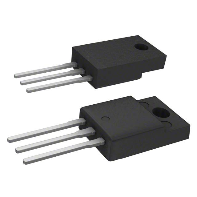
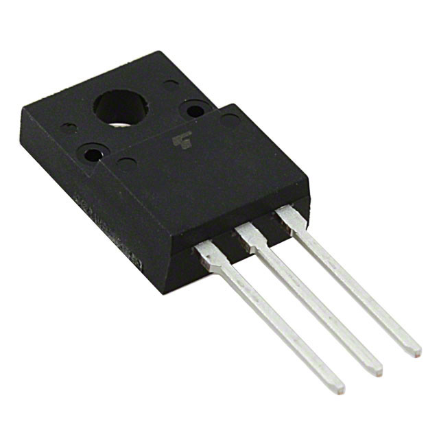
Package and Mounting: All substitute parts utilize through-hole TO-220 package variants (TO-220FM, TO-220FP, TO-220SIS) that are mechanically and electrically compatible with TO-220-3 Full Pack footprints.
Gate Voltage Rating (Vgs Max): All substitute parts maintain ±30V or ±25V maximum gate voltage ratings, ensuring compatibility with standard gate drive circuits.
The following substitute parts meet these criteria and are presented in order of electrical and operational compatibility.
Parameter Comparison
| Parameter | 2SK4085LS (Main) | TK13A45D(STA4,Q,M) | STP14NK50ZFP | STF11NM50N | STF14NM50N | R5011FNX |
|---|---|---|---|---|---|---|
| Manufacturer | onsemi | Toshiba | STMicroelectronics | STMicroelectronics | STMicroelectronics | Rohm Semiconductor |
| Drain to Source Voltage (Vdss) | 500V | 450V | 500V | 500V | 500V | 500V |
| Current - Continuous Drain (Id) @ 25°C | 11A (Tc) | 13A (Ta) | 14A (Tc) | 8.5A (Tc) | 12A (Tc) | 11A (Ta) |
| Drive Voltage (Max Rds On) | 10V | 10V | 10V | 10V | 10V | 10V |
| Rds On (Max) @ Id, Vgs | 430mOhm @ 8A, 10V | 460mOhm @ 6.5A, 10V | 380mOhm @ 6A, 10V | 470mOhm @ 4.5A, 10V | 320mOhm @ 6A, 10V | 520mOhm @ 5.5A, 10V |
| Gate Charge (Qg) (Max) @ Vgs | 46.6nC @ 10V | 25nC @ 10V | 92nC @ 10V | 19nC @ 10V | 27nC @ 10V | 30nC @ 10V |
| Vgs (Max) | ±30V | ±30V | ±30V | ±25V | ±25V | ±30V |
| Input Capacitance (Ciss) (Max) @ Vds | 1200pF @ 30V | 1350pF @ 25V | 2000pF @ 25V | 547pF @ 50V | 816pF @ 50V | 950pF @ 25V |
| Power Dissipation (Max) | 40W (Tc) | 45W (Tc) | 35W (Tc) | 25W (Tc) | 25W (Tc) | 50W (Tc) |
| Operating Temperature (TJ) | 150°C | 150°C | -55°C ~ 150°C | 150°C | -55°C ~ 150°C | 150°C |
| Mounting Type | Through Hole | Through Hole | Through Hole | Through Hole | Through Hole | Through Hole |
| Package / Case | TO-220-3 Full Pack | TO-220-3 Full Pack | TO-220-3 Full Pack | TO-220-3 Full Pack | TO-220-3 Full Pack | TO-220-3 Full Pack |
| Product Status | Obsolete | Active | Active | Active | Active | Not For New Designs |
| RoHS Status | — | ROHS3 Compliant | ROHS3 Compliant | ROHS3 Compliant | ROHS3 Compliant | ROHS3 Compliant |
Engineering Selection Recommendations
Primary Substitute: STF14NM50N
The STF14NM50N from STMicroelectronics is the recommended primary substitute for the 2SK4085LS. This device maintains the 500V drain-to-source voltage rating and exceeds the 11A continuous drain current requirement with 12A capability at 25°C. The STF14NM50N features improved on-state resistance (320mOhm) compared to the original part, resulting in lower conduction losses. The device is part of the active MDmesh™ II product line and carries ROHS3 compliance certification. Operating temperature range extends to -55°C, providing broader environmental compatibility. Gate charge is 27nC, slightly below the original specification, enabling faster switching transitions.
Secondary Substitute: STP14NK50ZFP
The STP14NK50ZFP from STMicroelectronics provides the highest current capability among substitute options at 14A continuous drain current. This device maintains 500V voltage rating and features the lowest on-state resistance at 380mOhm. The STP14NK50ZFP is part of the active SuperMESH™ product line with ROHS3 compliance. Extended operating temperature range (-55°C to 150°C) supports demanding thermal environments. Gate charge is elevated at 92nC, which may require driver circuit evaluation in high-frequency switching applications. Power dissipation capability is 35W, supporting higher thermal loads.
Tertiary Substitute: TK13A45D(STA4,Q,M)
The TK13A45D from Toshiba Semiconductor is an active product offering 13A continuous drain current with 450V voltage rating. While the voltage rating is 50V lower than the original specification, this device is suitable for applications where the 450V rating is acceptable. The part features 45W power dissipation capability and gate charge of 25nC, enabling efficient switching. ROHS3 compliance and active product status support long-term availability.
Alternative Substitute: R5011FNX
The R5011FNX from Rohm Semiconductor maintains 500V voltage rating and 11A continuous drain current, matching the original device specifications. This part carries ROHS3 compliance but is designated as "Not For New Designs," limiting its suitability for new development. The device offers 50W power dissipation capability, the highest among all substitutes. On-state resistance is 520mOhm, slightly elevated compared to the original part.
Lower Current Alternative: STF11NM50N
The STF11NM50N from STMicroelectronics is suitable for applications where 8.5A continuous drain current is sufficient. This device maintains 500V voltage rating and features the lowest input capacitance (547pF) and gate charge (19nC) among all substitutes, enabling rapid switching transitions. The part is active and ROHS3 compliant with extended operating temperature range (-55°C to 150°C). Power dissipation is limited to 25W, requiring thermal management evaluation in high-power applications.
Frequently Asked Questions (FAQ)
Q: Can the 2SK4085LS be directly replaced with any of these substitute parts?
A: Direct replacement depends on application-specific requirements. All substitute parts maintain 500V voltage rating (except TK13A45D at 450V) and support through-hole TO-220 mounting. However, differences in continuous drain current, on-state resistance, gate charge, and power dissipation must be evaluated against circuit design specifications. STF14NM50N and STP14NK50ZFP provide the closest electrical performance match for most applications.
Q: What is the difference between the TO-220FI(LS), TO-220FM, TO-220FP, and TO-220SIS packages?
A: All four package variants are TO-220-3 Full Pack configurations with identical pin assignments and through-hole mounting footprints. The suffix designations (FI, FM, FP, SIS) indicate manufacturer-specific package variants. These packages are mechanically and electrically interchangeable in standard TO-220 PCB layouts. Thermal performance and lead frame materials may vary slightly between manufacturers.
Q: Why does the 2SK4085LS have higher gate charge (46.6nC) compared to some substitutes?
A: Gate charge variation reflects differences in semiconductor technology and die design between manufacturers. Lower gate charge values (such as STF11NM50N at 19nC) enable faster switching transitions and reduced driver power consumption. Higher gate charge values require longer gate drive pulse widths but do not prevent substitution if the gate driver circuit has sufficient current capability and timing margin.
Q: Is the 450V rating of TK13A45D acceptable as a substitute for a 500V application?
A: The TK13A45D with 450V rating is suitable only for applications where the actual operating voltage does not exceed 450V. If the circuit design requires the full 500V safety margin, this device is not appropriate. Applications with maximum operating voltages below 450V can utilize this substitute.
Q: What is the significance of "Active" versus "Not For New Designs" product status?
A: "Active" status indicates the manufacturer continues production and supports long-term availability for new designs. "Not For New Designs" status indicates the manufacturer is phasing out the product and recommends alternative parts for new development. Existing inventory may remain available, but future procurement cannot be guaranteed. For new designs, select only parts with "Active" status.
Q: How do differences in on-state resistance (Rds On) affect circuit performance?
A: On-state resistance determines conduction losses when the MOSFET is in the on-state. Lower Rds On values reduce power dissipation and heat generation. For example, STF14NM50N at 320mOhm dissipates less heat than the original 2SK4085LS at 430mOhm. Higher Rds On values (such as R5011FNX at 520mOhm) increase thermal load and may require enhanced heat sinking or thermal management.
Q: Can I use STF11NM50N if my application requires 11A continuous current?
A: STF11NM50N is rated for 8.5A continuous drain current, which is below the 11A requirement. Using this device in an 11A application would exceed its continuous current rating and cause excessive junction temperature rise and potential device failure. Select STF14NM50N, STP14NK50ZFP, or TK13A45D for 11A or higher current applications.
Q: What is the impact of input capacitance (Ciss) on gate drive circuit design?
A: Input capacitance affects the gate charge required to switch the device and influences switching speed. Higher Ciss values (such as STP14NK50ZFP at 2000pF) require more gate charge and longer switching transitions. Lower Ciss values (such as STF11NM50N at 547pF) enable faster switching. Gate driver circuits must provide sufficient current to charge the input capacitance within the required switching time window.
Q: Are all substitute parts RoHS3 compliant?
A: All substitute parts listed carry ROHS3 compliance certification. The original 2SK4085LS does not specify RoHS status. RoHS3 compliance ensures the devices are free from restricted substances including lead, mercury, cadmium, and hexavalent chromium, meeting environmental and regulatory requirements for commercial and industrial applications.
Alternative Parts

SJ6012L2TP
Littelfuse Inc.
6 Alternative Parts

JMK107BBJ476MA-RE
Taiyo Yuden
10 Alternative Parts

GMK107BBJ475MA-T
Taiyo Yuden
5 Alternative Parts
SJ6020N2ARP
Littelfuse Inc.
3 Alternative Parts
SJ6025R2ATP
Littelfuse Inc.
4 Alternative Parts

2474-05L
API Delevan Inc.
1 Alternative Parts

4590R-684K
API Delevan Inc.
1 Alternative Parts

CM6560R-334
API Delevan Inc.
1 Alternative Parts

CM6460-104
API Delevan Inc.
1 Alternative Parts

5526-12
API Delevan Inc.
1 Alternative Parts