>
>


Product overview: STP14NK50ZFP STMicroelectronics MOSFET N-CH 500V 14A TO220FP
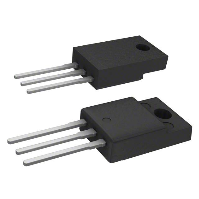
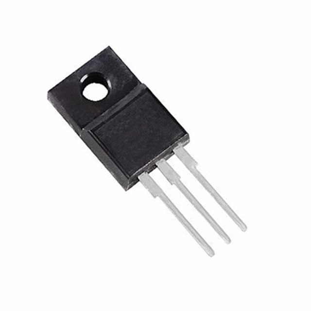
The STP14NK50ZFP is an N-channel MOSFET engineered for critical power switching requirements, combining advanced silicon process technology with design features that address the challenges typically encountered in high-voltage circuits. Rated at 500 V drain-source voltage and supporting a continuous drain current up to 14 A (Tc), this device effectively bridges the gap between conventional MOSFETs and specialized high-voltage switches by delivering reliable operation with substantial electrical headroom. The isolated TO-220FP package streamlines integration into power module architectures, alleviating the need for additional insulation measures in both primary and secondary sides of switching designs.
At the device physics layer, the STP14NK50ZFP employs optimized trench-gate structures and rugged silicon that minimize R_DS(on), yielding improved system efficiency through reduced conduction losses. The gate threshold and charge characteristics ensure sharp switching behavior, enabling fast transition times and precise control. Parasitic capacitances and stray inductance are also managed effectively by the package and die layout, reducing voltage overshoot and electromagnetic interference in fast-switching environments. This is particularly advantageous when soft-switching or snubber-less topologies are deployed.
Application engineering benefits are clearly observed in switched-mode power supplies (SMPS), motor drivers, and industrial inverters, where the combination of high current rating and substantial voltage withstand capability allows for designs pushing the limits of energy density and reliability. The fully isolated fin of TO-220FP facilitates direct mounting onto heat sinks without insulating pads, simplifying assembly in compact enclosures and reducing thermal impedance. This configuration enhances long-term durability in thermally stressed environments, where uniform heat dissipation and electrical isolation protect sensitive control circuits from transients and leakage currents.
Practical deployment often reveals the advantage of this MOSFET’s balanced parameter set: during in-circuit stress testing, devices remain stable under pulse loads close to maximum ratings, with predictable thermal behavior and minimal drift in key metrics. Such results are enabled by process-controlled gate oxide integrity and robust avalanche energy tolerance, which support transient handling in line filters or power factor correction stages with minimal degradation. Careful PCB layout—separating high-current and logic ground planes, controlling gate trace impedance—further exploits the MOSFET's intrinsic performance, reducing susceptibility to false triggering and cross-talk at high dV/dt.
Cross-application flexibility is evident in renewable energy inverters and battery chargers, where the inherent isolation and high voltage capacity encourage architectural choices that maximize system modularity. Integrating the STP14NK50ZFP into push-pull or full-bridge topologies allows circuit designers to address both the electrical and mechanical constraints with a single, reliable switch. Notably, the device’s consistency under repetitive stress cycles subtly highlights the value of tight silicon process control and package engineering in extending operational life. This convergence of electrical robustness, thermal management, and form-factor advantages positions the STP14NK50ZFP as a foundational component in next-generation, high-density power conversion systems.
Core features and technology of STP14NK50ZFP SuperMESH™ series
At the foundation of the STP14NK50ZFP SuperMESH™ series lies an intricate optimization of silicon structure, oriented to maximize performance in high-voltage power conversion. Leveraging the PowerMESH™ strip-based topology, SuperMESH™ technology employs advanced photolithography and fine cell pitch, resulting in exceptionally low R_DS(on) values—precisely 0.34 Ω for this device class. The physical arrangement of cells and reduction of interconnect losses are engineered to minimize carrier transit time, thereby streamlining conduction paths and curbing resistive losses under significant load conditions.
Critical to dynamic applications is the series’ minimized gate charge and intrinsic capacitance. Through refinement of oxide thickness and channel geometry, gated structures maintain ultra-low stored charge, directly enhancing switching speed and reducing switching losses. In practical contexts, this translates into lower thermal dissipation during rapid load changes. The device consistently sustains robust efficiency in demanding pulse-width modulation control loops, where gate drive limitations and turn-on/turn-off profiles can otherwise compromise system margins.
The SuperMESH™ layout inherently augments dv/dt ruggedness, exceeding stringent stability thresholds established for high-voltage transitions. This capability is validated by the device’s ability to reliably pass 100% avalanche test protocols. The inclusion of polysilicon gate reinforcements and source-drain clamping architecture underpins its endurance against overvoltage events, protecting critical circuits in switched-mode power supplies, motor control, and high-energy conversion modules.
An additional layer of assurance is derived from tightly controlled wafer fabrication processes. Uniformity in doping concentrations and layout symmetry ensures manufacturing repeatability, a cornerstone for deployment in mass-produced OEM designs. Such consistency stabilizes parametric spread, enabling designers to maintain tight tolerances in complex power trains and multi-phase systems.
In real-world engineering deployments, the STP14NK50ZFP’s fast transient response and robust avalanche capacity manifest as tangible reductions in component count for snubber and clamp circuits. Its thermal stability under repetitive switching stress fosters longer service intervals and simplifies thermal management, contributing to overall system reliability and ease of maintenance. The seamless interplay between minimized conduction losses and dynamic switching excellence exemplifies an optimized approach to discrete MOSFET integration in high-availability industrial and consumer systems.
Underlying these attributes is a philosophy of holistic device refinement—layering architectural, material, and process enhancements to anticipate and counteract operational stressors commonly encountered in evolving power electronic ecosystems. Such forward-looking integration not only raises the bar for efficiency and ruggedness, but also enables innovative topologies and compact system layouts, driving a step-change in what’s realizable with standard TO-220FP packaged MOSFETs.
Electrical ratings of STP14NK50ZFP STMicroelectronics MOSFET
Understanding and applying the electrical ratings of the STP14NK50ZFP MOSFET is fundamental for robust circuit design in high-voltage switching and power management environments. The device’s drain-source voltage (V_DS) of 500 V establishes its capability to handle demanding power topologies, such as offline converters, motor drive bridges, and industrial inverters. Ensuring V_DS never exceeds this threshold, especially during transient events—including inductive switching or line surges—prevents irreversible gate oxide or silicon breakdown. Protection measures, like snubber circuits and appropriately specified clamping diodes, are often deployed to absorb or limit voltage overshoots in practical hardware frameworks.
The continuous drain current (I_D) rated at 14 A (with case temperature referenced at Tc) underscores the device’s sustained load management in thermally controlled scenarios. Because current handling is highly temperature-dependent, monitoring the MOSFET’s case temperature during operation is pivotal. Excessive conduction or elevated switching frequencies increase the power dissipated in the silicon die, which, when not managed through low-impedance thermal design—typically via robust copper planes and heat-sinking—directly erode long-term reliability.
A distinction arises with the pulsed drain current. Unlike the steady-state I_D, the pulsed specification requires analyzing the safe operating area (SOA) curves provided in the datasheet, factoring in specific application pulse widths and duty cycles. For instance, in pulse-width-modulated (PWM) applications, leveraging the SOA chart is essential to avoid single-pulse or repetitive stress scenarios that exceed the silicon’s energy absorption capacity. Accurate current profiling in simulation and validation stages directly mitigates risk of avalanche or secondary breakdown modes, which can otherwise propagate device defects over time.
Maximum power dissipation, marked at 35 W (Tc), is a direct function of both ambient environment and board-level heat extraction efficiency. Real-world deployments demonstrate that the margin for error narrows rapidly if thermal interfaces are inadequately engineered or airflow is inconsistent. Employing thermal interface materials (TIMs) and matching the thermal expansion coefficients of board and package reduces mechanical stress and enhances junction reliability—a subtle detail often overlooked during prototype-to-mass-production transitions.
A particularly strong attribute of the STP14NK50ZFP is its rugged avalanche energy rating. The silicon process and device geometry confer high energy absorption capability during avalanche events, commonly triggered by inductive load switching or fault conditions. However, repeated or excessive energy surges, even below the absolute maximum, can incrementally degrade the device. Integrating advanced gate drive circuits and carefully matched external clamp elements, as experience in switched-mode designs suggests, yields significant lifetime extension and performance stability.
A notable insight is that the reliability envelope of power MOSFETs like the STP14NK50ZFP is rarely limited by static ratings alone; rather, application-induced dynamic stresses—especially thermal, avalanche, and switching transients—shape operational boundaries. Proactively profiling waveforms, validating heatsink and PCB design, and simulating extreme corner cases in both startup and fault regimes delivers the most robust architecture. Device characterization under real load conditions frequently reveals latent margin or constraint not apparent from datasheet ratings alone, allowing for more confident derating and protection scheme optimization in high-reliability installations.
Protection features in STP14NK50ZFP STMicroelectronics MOSFET
Protection features in the STP14NK50ZFP MOSFET center on an advanced gate-to-source zener diode configuration. This integration employs back-to-back zener structures directly across the gate and source terminals. At a fundamental level, this architecture establishes a robust clamp mechanism that limits gate voltage excursions. Critical during both ESD events and in-circuit switching transients, these zener structures conduct at a tightly controlled breakdown voltage, effectively safeguarding the sensitive gate oxide from overvoltage stress.
Embedded protection within the silicon itself ensures that any attempt by the gate voltage to exceed design thresholds results in immediate clamping action. This mitigates degradation mechanisms like time-dependent dielectric breakdown (TDDB) and prevents catastrophic gate puncture, which is often a failure mode when external transients go unchecked. The dual-parallel arrangement—back-to-back zeners—allows bidirectional handling of both positive and negative surges, offering comprehensive coverage as supply or signal polarity fluctuations occur.
The well-defined zener breakdown voltage is engineered to be just above the device’s maximum allowable gate voltage. This precision eliminates the common need for external zener diodes or TVS clamps, leading to a simplified PCB layout. In high-density power architectures, such integration is especially advantageous, as it not only reduces layout complexity but also minimizes parasitic inductances associated with discrete protection. With fewer external devices, BOM reduction translates to both lower cost and increased mean time between failure (MTBF).
Field applications in high-voltage inverters, motor drives, and PFC stages benefit directly from this feature. Typical transient waveforms induced by long cable runs or inductive load switching are effectively managed internally, preventing latent reliability issues, such as early-life failures or parameter drifts. Notably, the repeatability and stability of the protection threshold allow for confident system design—the zener action prevents unpredictable MOSFET behavior during commissioning and service events.
The integration of intrinsic gate protection in the STP14NK50ZFP reflects a trend toward smarter power device engineering. Instead of placing the burden on the system designer to factor in myriad fault contingencies, the device itself absorbs much of the complexity. One subtle but significant implication is the ability to leverage tighter gate drive strategies, extracting faster switching speeds without increasing gate stress risk. This supports more compact, efficient, and robust power stages, reinforcing the device’s suitability for demanding industrial environments where uptime and reliability are paramount.
Electrical characteristics of STP14NK50ZFP STMicroelectronics MOSFET
The electrical performance of the STP14NK50ZFP MOSFET from STMicroelectronics hinges on a finely engineered set of parameters that promote system-level robustness and efficiency. At the core, the device exhibits a low R_DS(on) value (typically 0.34 Ω at T_CASE = 25°C), a critical advantage for minimizing conduction losses in high-current environments. This becomes especially relevant in applications where reduced ON-state losses directly translate to lower heat dissipation constraints and improved overall power density. Such a characteristic simplifies thermal management and allows for tighter system-level efficiency margins.
The device’s fast switching behavior is a consequence of optimized internal charge structures, which enable rapid transitions between ON and OFF states without significant energy loss. This intrinsic speed is not solely a function of gate charge (Q_g), but also the result of reduced gate-to-drain and gate-to-source capacitances, which the manufacturer’s characteristic curves help quantify. When devising high-frequency switching circuits, the low total gate charge ensures rapid gate drive response, reducing delay and overlap losses. From practical implementation, attention to gate resistor sizing becomes essential to fully exploit the device’s switching capability while mitigating risks of voltage overshoot and electromagnetic interference.
Dynamic performance is further verified through transfer, output, and transconductance curves, which illustrate the device’s response under varied load and bias conditions. As these curves capture the MOSFET’s linear and saturation regions, they provide a practical foundation for load-line analysis and enable predictive modeling in power conversion and motor control topologies. Particularly under inductive loading, these characteristics assure designers of the device’s robustness against avalanche and safe-operating-area (SOA) violations—a frequent concern in hard-switching nodes or snubber-less topologies.
Thermal impedance scaling with pulse width and duty cycle is another dimension to consider during design-in, particularly in environments with high ambient temperatures or pulsed operation. The provided Z_th(j-c) curves guide layout optimization, heatsink selection, and thermal shutdown margining. Capacitance variation metrics, including C_iss, C_oss, and C_rss across voltage sweeps, inform snubber design and EMI filter tuning, ensuring that high dV/dt events are managed effectively.
The comprehensive datasheet should serve as an initial touchpoint, but true reliability and efficiency are realized through iterative prototyping and validation: aligning the MOSFET’s electrical behavior with the specifics of the application circuitry, gate drive configuration, and PCB parasitics. In power supply units, leveraging the device’s strengths results in cleaner switching edges and higher converter efficiency; in motor drives, it supports reliable torque delivery under variable loads. Attention to the nuanced interplay of thermal dynamics, switching, and SOA parameters unlocks the STP14NK50ZFP’s full potential in critical power and industrial designs.
Thermal and dynamic performance of STP14NK50ZFP STMicroelectronics MOSFET
The thermal behavior of the STP14NK50ZFP is defined by its TO-220FP package, with thermal resistance and impedance parameters directly influencing both instantaneous junction temperatures and long-term device reliability. The system-level impact of these parameters emerges in the context of rapid current surges and repeated switching events, commonly encountered in switching regulators or motor control units. Notably, the package’s isolated tab reduces parasitic capacitance but also necessitates careful heat dissipation, as thermal resistance from junction to ambient increases compared to standard TO-220 units. This necessitates precise heat sink selection informed by detailed thermal resistance metrics and standardized mounting conditions. In practice, lower thermal resistance values allow designers to maximize allowable current throughput without exceeding safe junction temperatures, while normalized performance graphs support nuanced derating strategies that align device ratings with specific operating environments.
Temperature dependencies outlined in the performance graphs—such as forward voltage drop and breakdown voltage shifting with ambient changes—underscore the necessity of incorporating thermal feedback loops within power management circuits. Accurate modeling of these effects leads to improved reliability predictions and more robust system designs. Effective PCB layouts for the STP14NK50ZFP often prioritize wide copper planes and minimize thermal bottlenecks, especially in densely populated board environments. Additionally, the integration of thermally conductive insulators between the package and the heat sink in prototypes can mitigate hot spots, preserving device longevity under continuous conduction states.
Dynamic attributes like gate charge and device capacitance offer a blueprint for fast and efficient system switching. Low total gate charge directly translates to reduced switching losses and enables deployment in high-frequency circuits where efficiency and thermal stability are at a premium. The interplay between gate-source voltage (Vgs) and gate charge is critical when dimensioning gate drive circuits: ensuring Vgs remains within optimal thresholds minimizes switching delays and suppresses unwanted oscillations. Capacitance characteristics, tracked across various drain-source voltages, reflect on the ability to manage voltage transients and electromagnetic interference (EMI). In practical high-speed applications, fine-tuning gate drive strength and leveraging snubber circuits have proven effective in reducing turn-on/turn-off time variability and minimizing ringing, further strengthening overall circuit resilience.
Switching waveforms and source-drain diode recovery profiles offer actionable insight into timing coordination within multi-MOSFET assemblies and synchronous rectifiers. Fast recovery and low reverse recovery charge parameters support tighter timing margins and increased efficiency, especially in resonant or soft-switching topologies. Experience shows the value in leveraging empirical waveform data to customize dead time intervals within digital controllers, facilitating maximum efficiency while suppressing shoot-through conditions. The device’s consistent reverse recovery behavior also simplifies paralleling multiple MOSFETs for increased current handling, as timing disparities are minimized.
Taken together, these thermal and dynamic attributes position the STP14NK50ZFP as a robust choice for high-efficiency, thermally demanding designs. Meticulous consideration of interface materials, system layout, and control strategies translates directly into tangible performance gains and reliability improvements, supporting wider deployment in advanced power electronics and demanding industrial contexts.
Test circuits for STP14NK50ZFP STMicroelectronics MOSFET evaluation
Test circuits developed for the STP14NK50ZFP STMicroelectronics MOSFET form the foundation for rigorous device evaluation and characterization. These circuit configurations address key operational aspects, including switching dynamics, gate drive behavior, and robustness under demanding load conditions. The switching time test circuit, optimized for resistive loads, quantifies turn-on and turn-off response, revealing intrinsic limitations imposed by device capacitance and gate resistance. By analyzing propagation delays and current transition rates in this setup, engineers can identify potential bottlenecks in high-frequency or fast-switching applications, guiding the selection of complementary gate drivers.
The gate charge measurement circuit isolates the charge-transfer profile during turn-on, delineating the required gate energy under both quiescent and dynamic regimes. This data proves indispensable for optimizing gate drive circuitry, especially in designs constrained by limited power budgets or where fast gate transitions are mandatory. Subtle variations in gate charge behavior, as observed under temperature or voltage deviations, can impact switching efficiency and thermal management strategies. Integrating these insights into hardware validation cycles ensures predictable behavior even under system-level stressors.
For endurance and ruggedness validation, the inductive load switching and diode recovery test environment evaluates avalanche capabilities, as well as reverse diode recovery characteristics. Captured waveforms expose the MOSFET's practical tolerance to overvoltage pulses and the dynamics of intrinsic body diode reversal. Controlled repetition of these tests under worst-case operating conditions reveals early signs of failure or abnormal transient behavior otherwise hidden in simplistic resistive analysis. Engineers routinely observe subtle correlations between device geometry, packaging, and recovery artifacts, which can influence reliability margins in inductive load commutation, motor drives, or flyback converter topologies.
The unclamped inductive waveform analysis focuses on device behavior under energy release scenarios, measuring voltage overshoot and current tailing with precision. This setup effectively simulates real-world circuit faults or inrush events, quantifying safe operating area margins and informing PCB layout improvements to suppress parasitic oscillations. Repeated stress cycles inform derating practices and spark data-driven revisions in snubber network design and trace geometry.
Deploying these targeted test circuits elevates the evaluation of the STP14NK50ZFP beyond datasheet compliance, facilitating tailored benchmarking aligned with system requirements. Insights gained from systematic characterization pinpoint design risks, validate simulation models, and streamline integration phases. Experienced practitioners leverage subtle test artifacts—such as waveform asymmetry or charge plateau formation—as early indicators of device suitability for controlled switching, power conversion, and protection functions in complex environments. Such a layered evaluation strategy enables efficient convergence from core physical characteristics to application-specific performance targets, establishing robust and predictable operation within final electronic assemblies.
Package and mechanical data for STP14NK50ZFP STMicroelectronics MOSFET
The STP14NK50ZFP MOSFET, produced by STMicroelectronics, is presented in the TO-220FP package, optimized for robust mounting and effective thermal management. This package integrates full electrical insulation between the tab and the internal silicon, minimizing the need for external insulators during assembly, and thus streamlining the mechanical design phase. The construction leverages a standardized footprint, which allows for direct placement into common PCB layouts, expediting integration when transitioning between compatible designs or scaling hardware production.
The physical profile of the TO-220FP fosters reliable heat dissipation in environments demanding sustained performance, balancing reduced thermal resistance with compact dimensions. The mounting holes and flat tab geometry facilitate firm attachment to heat sinks or chassis elements, and the fully isolated tab substantially reduces the risk of inadvertent short circuits and simplifies safety validation, particularly in high-voltage sections.
PCB footprint recommendations provided by STMicroelectronics consider critical factors including creepage and clearance distances, especially relevant in power applications exceeding several hundred volts. The footprint dimensions support automated soldering processes, maintaining pad geometries compatible with both reflow and wave soldering techniques. Experience integrating these MOSFETs reveals that careful attention to solder mask expansion and thermal via placement can further mitigate hotspots observed during accelerated load cycling, an observation that informs layout refinements for increased operational longevity.
Environmental compliance is established through ECOPACK® certification, directly aligning the MOSFET’s materials with global lead-free directives as regulated by JEDEC JESD97. This approach not only addresses regulatory requirements but also reduces downstream quality management overhead for products entering international markets. The reliability of lead-free terminations in high-power circuits is substantiated by enforced process controls during fabrication, yielding surfaces that withstand multiple soldering cycles without significant degradation or shift in electrical performance.
For high-volume production or automated line deployment, STMicroelectronics supports various shipment formats—while the TO-220FP typically comes in tray packaging, other variants in the same MOSFET family offer tape-and-reel options suited for pick-and-place automation. This enables scalable assembly workflows, critical for mass production scenarios requiring tightly controlled inventory and process optimization.
A subtle but crucial engineering insight involves leveraging the TO-220FP’s insulation for multi-device parallelization in closely packed layouts, where device reliability is paramount and board real estate is constrained. High-voltage power conversion architectures benefit from the isolation, preventing parasitic paths and facilitating the deployment of compact, efficient switching stages that remain electrically safe. This strategic use of package design can be a differentiator in systems where performance and regulatory compliance are tightly coupled, driving value across both prototyping and commercialization stages.
Environmental compliance and reliability of STP14NK50ZFP STMicroelectronics MOSFET
The STP14NK50ZFP from STMicroelectronics exemplifies robustness in both environmental compliance and operational reliability, underpinning its suitability for applications demanding stringent quality standards. At the foundational level, the device achieves Moisture Sensitivity Level 1 classification, indicating complete resistance to moisture-related degradation not only during reflow soldering but also throughout extended storage, shipment, and assembly processes. This characteristic is vital for electronics manufacturing environments, as it simplifies supply chain logistics—devices can be exposed to ambient conditions without strict sealing or baking requirements, reducing process complexity and overhead.
From a regulatory standpoint, the MOSFET maintains a REACH unaffected status, signifying absence of restricted substances and thereby satisfying chemical safety mandates across European production markets. This aligns with the evolving demands for eco-friendly electronics, increasingly preferred in sectors such as industrial power and automotive control, where component traceability and lifecycle management are tightly regulated. The EAR99 export designation further streamlines international distribution, circumventing burdensome licensing while ensuring unrestricted transfer to most markets. Compliance with HTSUS 8541.29.0095 enhances transparency in customs categorization, expediting cross-border logistics and minimizing interruptions in time-sensitive manufacturing cycles.
Integrating these compliance layers directly impacts downstream reliability in end-products. In assembly scenarios with aggressive soldering profiles or high ambient moisture, the risk of latent defects—such as internal corrosion or package delamination—is decisively mitigated. This reliability is reflected in field performance, where deployed systems exhibit lower failure rates and reduced maintenance cycles, supporting strong total cost-of-ownership metrics in industrial and infrastructure applications. Notably, sourcing this device alleviates burdens on procurement and quality assurance teams by harmonizing with broad regulatory frameworks, thereby fostering project scalability without recurrent documentation or certification bottlenecks.
From an engineering perspective, the convergence of rigorous moisture immunity and multi-jurisdictional compliance confers unique strategic advantages. Product designers can confidently standardize on the STP14NK50ZFP across geographically distributed production sites, knowing it will pass regulatory audits and withstand diverse operating environments. Experience in high-power switching circuits confirms that integrating such components leads to not only technical reliability but also administrative efficiency over multi-year production cycles, setting a benchmark for dependable and compliant semiconductor deployment.
Potential equivalent/replacement models for STP14NK50ZFP STMicroelectronics MOSFET
A thorough evaluation of potential equivalent or replacement models for the STP14NK50ZFP from STMicroelectronics begins with an analysis of the underlying device architecture and precise electrical characteristics. The primary candidates—STP14NK50Z, STB14NK50Z, STB14NK50Z-1, and STW14NK50Z—share closely matched silicon die and core parameters, reflected in their drain-source voltage ratings, R_DS(on), and current handling capabilities. These devices are built upon the same rugged planar technology, ensuring similar avalanche energy performance and safe operating area profiles. This commonality enables seamless substitution from an electronic standpoint, provided the secondary parameters align with the application’s stress envelope.
Mechanical considerations introduce significant variables. The suffixes—FP, Z, B, W—denote package formats such as TO-220FP, TO-220, D^2PAK, and TO-247 respectively. The choice must reflect the board layout constraints, heat dissipation strategy, and insulation requirements. For instance, the TO-220FP offers full encapsulation with isolated mounting surfaces ideal for safety-critical or compact systems, whereas the TO-247 variant supports higher thermal loads through improved heat sinking, albeit necessitating external insulation for high-voltage assemblies. In practice, subtle disparities in lead geometry, pad spacing, or mounting hole positions can require minor adaptations in footprint or requalification of automated assembly routines. Observing these tangential dimensions preempts production delays and simplifies validation.
It is essential to scrutinize environmental and certification parameters for equivalent model selection. Variants should be compared for compliance with existing agency marks (UL, IEC), MSL ratings for reflow soldering, and RoHS cadence. Substituting between models within the same series generally retains shared certifications, yet even identical dice can carry nuanced differences in qualification lot or test conditions. System designers frequently capitalize on manufacturer-provided cross-qualification certificates to expedite substitution while maintaining regulatory documentation, especially when pursuing drop-in replacement in certified platforms.
Direct experience has proved the merit of maintaining a preferred device matrix covering alternative packages. This approach streamlines procurement resilience and accelerates fault recovery under component shortage scenarios, offering practical flexibility without compromising system reliability. On numerous projects, careful mapping of alternate package equivalents has led to reduced bill-of-material complexity and minimized tooling adjustments, reflecting a best practice in both prototyping and volume deployment.
A unique insight arises when considering thermal management in high-power circuits. Empirical observation reveals that MOSFET performance converges under controlled ambient conditions, yet package-related thermal impedance can result in substantial divergence under elevated stress or confined form factors. As such, simulation and bench verification of junction temperatures across package variants deliver actionable data for final device selection, supplementing datasheet comparisons.
In summary, the selection of an STP14NK50ZFP equivalent demands a nuanced assessment—technical parity at the die level is foundational but only part of the equation. Detailed understanding of package characteristics, board-level integration, qualification trail, and real-world thermal working points enables optimal device interchangeability, aligning theoretical equivalence with application-specific robustness and long-term maintainability.
Conclusion
The STP14NK50ZFP SuperMESH™ MOSFET leverages advanced planar process technology, enabling both low on-resistance and high avalanche ruggedness. This combination is achieved through precise gate engineering, optimizing channel geometry and doping profiles to minimize conductive losses without compromising breakdown voltage. The logic-level gate drive facilitates integration in systems where gate control headroom is limited, enhancing compatibility with modern low-voltage logic devices. These underlying mechanisms collectively address the stringent requirements of industrial switch-mode power supplies, motor drives, and auxiliary switching circuits subjected to repetitive high-stress events.
Thermal management emerges as a critical consideration in field deployments. The I2PAK package provides an effective heat dissipation path, yet junction temperatures must be maintained well below absolute maximum thresholds to prevent performance drift or device failure. Practical deployment favours the use of multi-layer PCBs with dedicated thermal vias and copper pours optimally configured for the mounting footprint. In high-density assemblies, forced air cooling in combination with robust heatsink attachment can substantially extend operational lifetimes, mitigating hotspots that might otherwise induce early device degradation.
Electrical coordination requires a detailed approach to both gate drive design and fast switching transient control. Adequate gate resistance selection, tailored to the specific board layout and stray inductance values, suppresses undesired oscillations and eliminates shoot-through risks in half-bridge configurations. Snubber networks may be introduced at the PCB design stage to absorb voltage overshoot, especially when operating in environments with frequent inductive load switching. In these scenarios, close attention to the device’s dv/dt rating ensures repeatable operation free from parasitic turn-on events.
Switching performance directly influences power conversion efficiency, especially at elevated frequencies. The inherent fast switching edge presented by the SuperMESH™ cell architecture allows for reduced dead times in synchronous topologies, yielding improvements in converter efficiency and thermal margins. This characteristic is particularly relevant in compact power modules where both board space and cooling resources are at a premium. Experience shows that minor gate drive refinement—such as optimally tuning the gate resistor based on empirical waveform analysis—often unlocks incremental efficiency gains not attainable through datasheet-driven design alone.
Engineering choices must address not only core electrical and thermal performance but also compliance with regulatory and environmental standards. RoHS and REACH compliant packaging, as well as robust avalanche energy ratings, position the STP14NK50ZFP for deployment in geographically diverse markets and hostile field conditions. When alternate package types or assembly flows are dictated by system constraints, the broader STMicroelectronics MOSFET portfolio offers direct pin-compatibility and electrical migration paths, greatly easing platform upgrades and extending product line longevity.
Ultimately, this device’s balance of fast switching, low conduction losses, and ruggedization streamlines high-stress application design, enabling compact, efficient, and reliable solutions across a spectrum of power engineering challenges. The nuanced application of thermal and gate drive optimization, layered with compliance considerations, ensures robust system integration and future scalability.