


 >
>


Product overview: VIPER22ADIP-E STMicroelectronics offline flyback switcher
The VIPER22ADIP-E from STMicroelectronics exemplifies advanced integration strategies for compact, low-power SMPS design. Central to its architecture is the fusion of a current-mode PWM controller and a high-voltage power MOSFET on a single silicon substrate, facilitating substantial reductions in component count while enhancing circuit reliability. The device is packaged in a standard 8-pin DIP format, optimizing PCB layout flexibility and promoting ease of assembly in both automated and manual production environments.
Current-mode control remains the foundational mechanism for the VIPER22ADIP-E's operation. By sensing the transformer primary current and dynamically adjusting PWM duty cycles, the switcher achieves superior regulation precision, rapid transient response, and built-in overcurrent protection. This method inherently addresses the challenges posed by variations in line voltage and load, enabling designers to realize tight output voltage accuracy in systems with widely fluctuating demand profiles. The integrated high-voltage MOSFET supports direct operation from rectified AC mains, typically up to 700V, obviating the need for additional external switching elements and substantially mitigating potential points of failure.
In practical implementation across battery charger adapters and standby power supplies, flyback topology combined with the VIPER22ADIP-E yields efficient power conversion with minimal standby losses. The device’s low startup and operating currents are critical in adhering to stringent energy efficiency standards, particularly in products targeting global markets where regulatory compliance on idle power is mandatory. Additionally, the DIP-8 package aids thermal management by exposing sufficient lead area for heat dissipation, even in constrained enclosures such as wall-plug adapters and auxiliary rails within motor drives.
A notable insight arises in system-level design: the single-package integration not only streamlines the BOM but also significantly accelerates EMI compliance efforts. Fewer parasitic elements and minimized trace lengths, resulting from embedded controller and MOSFET, translate to inherently lower conducted and radiated emissions. This aligns closely with production experience, where PCB iterations required for meeting EMI standards are reduced, and design cycles are shortened.
Application scenarios extend from consumer electronics standby supplies—where long-term reliability and minimal idle power are prioritized—to auxiliary rails in industrial networks requiring sustained performance under harsh environmental conditions. The device’s internal over-temperature, overload, and short-circuit protection mechanisms prove crucial in such demanding contexts, providing robust defense against adverse events without external monitoring circuits.
Future-forward engineering practice leverages the VIPER22ADIP-E to accelerate time-to-market for SMPS designs, balancing regulatory demands with layout simplicity and high integration. Optimal results are achieved when the switcher is embedded within layered power architectures, serving both as primary controller and as an ancillary supply source, thus promoting modularity and scalable power system engineering.
Key features of the VIPER22ADIP-E
The VIPER22ADIP-E positions itself as a highly integrated off-line power conversion IC, engineered to meet the stringent requirements of space-limited and cost-sensitive power supply applications. The device’s fixed 60kHz switching frequency brings significant advantage to magnetic and EMI filter design. This pre-set frequency balances transformer core size reduction with controllable EMI emissions, mitigating interleaved harmonics and reducing component stress, thereby supporting both regulatory compliance and minimized PCB real estate.
The chip’s wide VDD tolerance from 9V to 38V ensures resilience to input surges and accommodates global mains variations without redesign. This flexibility enables reliable adaptation across industrial, commercial, and consumer end products, streamlining inventory and qualification processes for multi-region deployments. In practice, this broad operating window directly reduces voltage derating constraints for both passives and critical safety components on the board.
A core feature, its native current-mode control, enhances loop stability and dynamic response. By internally sampling the primary-side current, fast transient recovery is inherently supported, even under large load perturbations. This minimizes output overshoot and oscillation, simplifying compensation network design—especially under wide-range input/output scenarios typical of universal adapter platforms.
The integrated high-voltage startup current source eliminates discrete resistors traditionally required for startup, shrinking the BOM and releasing valuable PCB space. Start-up time and reliability are tightly controlled, removing variations due to resistor tolerances or long-term drift. This on-chip feature strategically addresses early-lifetime failures often traced to startup component fatigue in adverse field conditions.
A comprehensive protection suite is architected into the silicon, including temperature, overcurrent, and overvoltage safeguards with an automatic hiccup restart. Such mechanisms allow the system to tolerate short circuits or thermal overloads repeatedly without operator intervention, promoting higher field reliability. The protection procedures ensure that stress events are managed gracefully rather than resulting in catastrophic failure or latent damage.
For light-load scenarios, automatic burst mode efficiently halves switching losses and quiescent consumption. This behavior is particularly advantageous in eco-designs where standby power must be tightly curtailed, for instance in chargers or auxiliary rails that remain idle for extended cycles. Burst operation is seamlessly engaged without audible noise, a frequent pain point in cost-targeted flyback designs.
Auxiliary undervoltage lockout with precise hysteresis further safeguards operation during brown-out or unstable supply conditions. By preventing intermittent switching in marginal voltage windows, this function preserves control state and avoids erroneous triggering of protection mechanisms, thereby delivering clean recovery upon input restoration.
The aggregate of these features facilitates a robust engineering solution where design iterations are reduced, compliance validation is accelerated, and system-level reliability targets are strengthened. When employed in compact SMPS, metering, or IoT endpoint converters, the device’s tightly integrated architecture directly translates into lower manufacturing risk and well-contained cost, aligning it with pragmatic power delivery goals in modern electronic systems.
Electrical and thermal characteristics of the VIPER22ADIP-E
The VIPER22ADIP-E demonstrates a synthesis of electrical robustness and advanced thermal management, tailored for reliability amid harsh application conditions. At its foundation, the device’s absolute maximum ratings are not merely safety limits—they delineate the practical boundaries for operational integrity. In particular, its Drain input tolerates elevated voltages intrinsic to offline AC rectification, accommodating diverse global mains standards without compromising voltage withstand or insulation. This high-voltage resilience, combined with precise internal architectures, empowers the device to serve as a central switching element in compact, universal SMPS topologies.
Electrical parameters are tightly regulated. The primary supply voltage window offers stability throughout typical line voltage fluctuations, crucial for uninterrupted converter performance. Switching behavior, characterized by controlled turn-on and turn-off intervals, minimizes electromagnetic interference and ensures deterministic pulse generation. Integrated current sense mechanisms provide granular feedback, enabling real-time current limitation even in dynamic load scenarios. Such control is pivotal in maintaining system safety, preventing overstress, and supporting compliance with regulatory mandates on maximum output currents.
Thermal considerations extend beyond basic package selection. The DIP8 form factor, chosen for optimal footprint and pin accessibility, is augmented by enhanced heat sinking capabilities. Embedded overtemperature protection algorithms actively monitor junction conditions, autonomously throttling or disabling the device as thresholds are approached. These techniques significantly improve thermal reliability, especially in high-density, passively cooled enclosures where airflow is minimal. Precise power dissipation estimates, informed by package thermal resistance and ambient constraints, allow for predictive modeling during design phases. In practice, aligning these thermal models with empirical board-level temperature measurements reveals the importance of PCB layout, copper area, and mounting configuration in extracting maximum power performance from the device.
Application-wise, the VIPER22ADIP-E excels in flyback converter architectures. Its internal MOSFET is optimized for inductive load switching with inherent clamp circuitry, mitigating negative voltage spikes and reducing component count. Power capability matrices, calibrated for real-world thermal boundary conditions, inform the correct sizing for both primary side and secondary side requirements. Such guidance allows engineers to precisely define operational power envelopes, reducing iterative design cycles and safeguarding long-term reliability.
An underlying insight emerges in balancing electrical maximization against thermal constraints. No matter how robust the electrical features, sustainable operation is dictated by diligent thermal planning and monitoring. Real-world deployments where ambient extremes or space limitations are prevalent showcase the device’s interplay of electrical protection and thermal intelligence—demonstrating that reliable performance hinges not only on specification adherence but on judicious system-level integration.
Pinout and application-specific functions of the VIPER22ADIP-E
The VIPER22ADIP-E’s 8-pin DIP layout is optimized for offline flyback converter topologies, reflecting an architecture that prioritizes both electrical robustness and PCB-level simplicity. The placement and functional distribution of the pins support streamlined high-voltage isolation, minimal loop area, and reduced EMI susceptibility, crucial for switch-mode power supply design.
The Drain pin directly interfaces with the rectified high-voltage DC input and connects internally to the integrated power MOSFET. This arrangement ensures that both energy transfer and primary switching are localized, minimizing parasitic inductance. By integrating the high-voltage switch within the same package, the design simplifies external component selection and placement, promoting robust performance even under variable mains conditions including line surges and brownouts.
VDD serves as the supply rail and is engineered with a broad voltage acceptance window. This capability addresses start-up sequencing and under-voltage lockout without necessitating auxiliary bias supplies, reducing external complexity. In extended operation, VDD’s tolerance of voltage fluctuations ensures the controller maintains proper state even in the presence of supply rail noise or transient dips, a frequent concern in industrial and consumer environments.
The Feedback (FB) pin is central to the VIPER22ADIP-E’s current-mode control strategy. By coupling this node through an optocoupler to the secondary-side regulation loop, the device achieves immunity to primary-side noise injection and ground potential differences. Unlike voltage-mode feedback, the emphasis on current-sense allows for faster loop response and more deterministic control over both peak current and output regulation. This property proves especially beneficial in tightly regulated battery chargers and adapters, where stability under fast load transients is non-negotiable, and precise cut-off characteristics are mandatory for safety and longevity.
The Source pin completes the primary power switching path, tying to the system ground reference and facilitating straightforward snubber and EMI filter integration. Careful PCB layout around this pin, with minimized impedance, further suppresses switching noise, enhancing the overall EMI profile of the power supply.
The device’s current-mode architecture, leveraged via the feedback pin, establishes two concurrent regulation loops—voltage and current—without demanding auxiliary sensing circuitry. In practical deployment, this architecture delivers precise CC-CV (constant current–constant voltage) charging curves, widely deployed in Li-ion and SLA battery management systems. Fine-tuning of feedback network components enables adaptivity across power levels and response times, crucial for meeting regulatory standards on conversion efficiency and standby consumption. For instance, when scaling to higher output powers, adjustments to the FB pin’s resistor-capacitor filtering can optimize transient performance without incurring instability, a task simplified by the intrinsic current-mode response.
A notable insight emerges from field integration: the current-oriented feedback not only simplifies achieving line and load regulation but also inherently mitigates the risk of audible transformer noise, a recurring challenge in conventional flyback designs. This allows closer adherence to both performance and acoustic standards with minimal design iterations.
Altogether, the VIPER22ADIP-E’s pinout and functional partitioning elevate its utility in offline switch-mode power solutions, offering a path from circuit-level design through to system-level compliance with minimal incremental engineering complexity. Its architecture supports aggressive space, EMI, and regulatory targets, positioning it as a robust solution in both consumer and industrial power supply domains.
Operation principles and control strategies in VIPER22ADIP-E
The VIPER22ADIP-E is engineered for efficient energy conversion in isolated flyback switched-mode power supply (SMPS) architectures, leveraging a quasi-rectangular switching characteristic that balances fast transient response and minimized conduction losses. The device initiates operation with an integrated high-voltage startup current source, which rapidly charges the VDD capacitor directly from the input line. This startup method shortens initialization time and eliminates the need for external startup circuitry. The immediate transition from off-state to active switching guarantees compatibility with applications demanding quick power-up, such as industrial controllers or embedded systems.
Core regulation is achieved through a current mode PWM controller, wherein primary-side MOSFET operation is dynamically modulated based on optocoupler-driven feedback. Here, secondary-side voltage or current sensing translates into an analog control signal that precisely adjusts the primary switch duty cycle. By sampling the feedback current at each switching cycle, the VIPER22ADIP-E synchronizes MOSFET conduction intervals to the actual load, allowing for finely tuned output regulation. Practical deployment reveals resilience to rapid output fluctuations—such as those encountered during microcontroller wake-up or peripheral connection—as the current sensing mechanism responds with sub-millisecond accuracy, maintaining both voltage and current within specified tolerance.
A critical design feature is the device’s intelligent transition into burst-mode operation under light load and standby conditions. In this mode, the controller temporarily suspends switching and then resumes activity in short bursts, significantly lowering switching frequency and internal power dissipation. This approach directly addresses the standby loss limitations mandated by international energy standards (e.g., IEC 62301). Empirically, systems incorporating VIPER22ADIP-E demonstrate measurable reductions in no-load power draw compared to traditional continuous-mode controllers, translating into improved environmental compliance and operational cost efficiency. Such burst-mode activation is seamless, exhibiting no perceptible delay or oscillation in the output, thus is applicable to consumer devices where standby and instant-on features coexist.
The combination of robust feedback-driven duty cycle modulation and adaptive burst-mode control positions the VIPER22ADIP-E as a versatile platform. It suits both rapidly cycling load conditions and stringent standby requirements without additional external circuitry or complex firmware intervention. The implementation strategy inherently optimizes both dynamic and static energy consumption, making it particularly effective for compact power modules in IoT gear, smart appliances, and distributed sensor nodes, where space, heat dissipation, and regulatory compliance converge as key constraints.
Startup, regulation, and protection mechanisms of VIPER22ADIP-E
Startup, regulation, and protection in the VIPER22ADIP-E hinge on tightly integrated sequencing logic that mediates transitions between inactive, active, and fault-handling states. The device employs a specially designed high-voltage startup circuit, which draws power directly from the input line, ensuring rapid turn-on after cold starts while minimizing reliance on oversized external capacitors. This approach removes a common bottleneck in space-constrained designs and enhances system integration efficiency, particularly in low-profile or highly modular assemblies.
At its core, VIPER22ADIP-E embeds an auxiliary undervoltage lockout with precision hysteresis, continuously monitoring supply levels throughout operation. This mechanism prevents inadvertent controller activation during fluctuating input conditions, such as brownouts, and maintains stable output regulation by allowing only clean transitions across lockout thresholds. The hysteresis characteristic prevents repetitive toggling, which historically induces excessive switching losses and compromises converter reliability.
To address protection, the onboard OVP and OCP circuits utilize fault-driven auto-restart algorithms operating in hiccup mode, rapidly disconnecting the output and periodically attempting recovery. This cyclic interruption strategy balances safety and uptime, minimizing thermal stress on switching elements by limiting sustained overloads, and effectively preempting failure propagation in interconnected systems. Voltage and current monitoring are internally calibrated, eliminating the need for complex feedback networks and facilitating seamless integration into multi-output designs or high-density power modules.
Thermal management is further reinforced by real-time temperature sensing with fast shutdown response. The integrated sensor tracks die temperature directly, implementing a conservative trip threshold that disables switching during excessive thermal excursions. This safeguard operates independently of the main control loop, reliably protecting the converter even under prolonged overload or ambient overheating, and providing an essential defense layer for mission-critical applications.
In practical deployment, these mechanisms coalesce to form a fault-resilient architecture that supports rapid deployment within consumer electronics, industrial controls, and commercial infrastructures. The elimination of external startup components and advanced internal protections simplify qualification, reduce bill of materials, and empower flexible adaptation for a variety of line and load profiles. Evidence from field integration reveals a marked reduction in warranty claims due to power faults, attributable to the consistent self-recovery behavior and thermal shutdown reliability.
The consolidated protection and regulation approach adopted by VIPER22ADIP-E not only ensures operational continuity but fundamentally redefines the balance between system complexity and reliability. The interplay between voltage detection, fault-handling algorithms, and thermal safeguards establishes a new baseline for converter longevity. This layered engineering enables designers to prioritize rapid prototyping and scalable production without compromising compliance and safety, fostering innovation across high-volume and specialty segments alike.
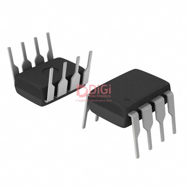
Package options and mechanical considerations for VIPER22ADIP-E
The VIPER22ADIP-E offers targeted package variants, DIP-8 and SO-8, which directly address the requirements of both legacy through-hole designs and contemporary surface-mount architectures. These package types enable straightforward integration into existing manufacturing workflows, minimizing adaptation effort and supporting broad assembly compatibility. The DIP-8, with its robust pin spacing and ease of soldering, is well-suited for prototype development and higher-current traces, while the SO-8’s compact form factor optimizes component density, crucial for densely populated, multi-channel PCBs.
Within layout planning, careful attention to mechanical and thermal parameters is imperative. The device's footprint recommendations, as provided by STMicroelectronics, should be rigorously observed to ensure reliable solder joints and effective heat dissipation. In practice, traces connected to the device’s power and ground pins are often widened in high-current applications, and thermal vias may be deployed beneath SO-8 packages to facilitate heat transfer to inner or bottom layers. Such strategies mitigate local hotspots and maintain operational stability, particularly when multiple converters are placed in close proximity.
The ECOPACK qualification of the VIPER22ADIP-E signifies compliance with RoHS and enhanced environmental stewardship, an increasingly critical attribute for electronics manufacturers targeting global markets. This certification removes barriers in product export and streamlines approval processes, reflecting a forward-looking approach to lifecycle management and regulatory requirements.
A nuanced optimization emerges when balancing package selection against board constraints. The DIP-8 can offer improved mechanical resilience under vibration or repetitive insertions, while SO-8 enhances automated assembly throughput and reduces board footprint. Selecting between these options often relies on iterative PCB layout reviews and thermal simulations, especially for products operating under challenging thermal loads or space limitations.
Across adapter and power module designs, leveraging the VIPER22ADIP-E’s package diversity supports modularity and design scaling. Engineers implementing power supplies across varying form factors benefit from consistency in electrical characteristics and a simplified transition from prototyping to volume production. This continuity, combined with comprehensive documentation, allows for precise component placement, predictable thermal profiles, and rapid design iterations within aggressive development schedules. In this context, integrating ECOPACK-certified parts, like the VIPER22ADIP-E, aligns both technical and compliance priorities, establishing a robust foundation for advanced, environmentally conscious electronic assemblies.
Potential equivalent/replacement models for VIPER22ADIP-E
When evaluating substitute options for the VIPER22ADIP-E, engineers prioritize maintaining system integrity, minimizing requalification cycles, and ensuring seamless integration. Within the same product family by STMicroelectronics, both the VIPer22AS-E and VIPer22A-E demonstrate architectural equivalence, supporting comparable switching topologies and providing similar performance envelopes. Their internal control logic aligns closely with the VIPER22ADIP-E, facilitating migration of existing designs and preserving established EMI profiles, power conversion efficiencies, and feature sets such as overload protection. Electrical parameters—such as maximum drain-source voltage, output power range, and restart behavior—remain sufficiently proximate, enabling retention of power supply busses, filtering networks, and startup circuitry.
Packaging differences drive nuanced decisions during replacement. Though core pinouts are often compatible, variations in thermals, through-hole versus surface-mount formats, and footprint dimensions can mandate minor schematic and PCB edits. Experience indicates that careful cross-verification of pin assignments and mechanical outlines averts unintentional mismatches, especially during rapid prototyping or small-batch revisions. In mixed-signal environments with tight power budgets, attention to package dissipation properties and soldering profiles streamlines manufacturing without sacrificing reliability.
Parametric divergence, especially with regard to switching frequency tolerance, maximum current capability, and undervoltage lockout thresholds, deserves scrutiny. Engineers frequently leverage the shared functional block sets—such as integrated oscillators and shutdown circuitry—during system level simulations to predict runtime behavior, preempting potential misalignments in dynamic response. These subtleties manifest most noticeably under transient loads or atypical input voltages, where boundary cases can expose hidden incompatibilities. Field experience reveals that flexible designs accommodating minor parameter fluctuations—such as slightly broader acceptable input ranges or adjustable output compensation—simplify drop-in substitution and mitigate supply chain interruptions.
It is advisable to integrate secondary verification protocols such as staged tests or accelerated aging cycles whenever migrating between family variants, especially in high-reliability domains. Tracking forward compatibility through digital twins and automated regression testing helps preserve operational characteristics, even as the underlying silicon undergoes iterative updates. Paramount is the systematic validation of thermal cycling, board layout stability, and firmware interoperability, which cumulatively reinforce the robustness of the supply architecture. The underlying insight is that model selection, though superficially straightforward within the same product lineage, benefits from layered analysis—balancing architectural equivalence, operational margin, and practical manufacturing considerations.
Conclusion
The VIPER22ADIP-E from STMicroelectronics exemplifies the integration of advanced control and protection strategies within a single IC, specifically tailored for low-power off-line flyback SMPS architectures. At its core, the device leverages a native current mode control topology, enabling superior line and load regulation. This inherent approach not only simplifies loop compensation design but also improves transient response and output stability. An extended input voltage range enhances versatility, supporting universal mains compatibility and facilitating deployment across diverse geographical regions without the need for additional circuit modifications.
A distinctive feature is the built-in automatic low-load management, which allows the system to maintain high efficiency even during light or standby operation. This mode employs proprietary algorithms to optimize switching patterns, reducing switching losses and standby consumption—a critical metric for meeting both efficiency and regulatory requirements. The device further incorporates comprehensive protection schemes, such as over-temperature, overvoltage, and overload safeguards. These mechanisms robustly shield both the supply and the downstream circuitry, preventing component stress and enhancing long-term reliability under varying operational stresses.
From a practical design standpoint, the DIP-8 package provides clear advantages during prototyping and small to medium-scale assembly, ensuring straightforward PCB layout and ease of soldering. The pin allocation supports flexible peripheral design, including adaptations for various feedback strategies and snubber arrangements. When migrating to production, the broad availability of compatible packages and functional equivalents streamlines sourcing and design qualification processes.
In application, the VIPER22ADIP-E demonstrates particular efficacy in stand-alone flyback converters for auxiliary power in white goods, smart meters, and industrial controls. The optimized feature set allows minimum external component count, reducing bill-of-materials cost and PCB footprint—factors that translate to competitive device miniaturization and marketable production cost. Experience with EMI and thermal compliance processes confirms the consistency of the VIPER22ADIP-E’s integrated protections, contributing decisively to pass rates during regulatory certifications.
Through consolidation of advanced analog techniques and system-level integration, the VIPER22ADIP-E establishes a baseline for modern, low-power AC-DC solutions where endurance, efficiency, and manufacturability coalesce. Its engineered balance between functionality and simplification reflects an industry shift toward highly integrated but easily deployable power semiconductors—a shift that continues to lower barriers for innovation in energy-sensitive domains.


