


 >
>


Product overview: VIPER122LSTR high voltage converter from STMicroelectronics
The VIPER122LSTR from STMicroelectronics is architected for high-voltage offline power conversion, uniting a robust 730 V avalanche-rated MOSFET and precision PWM controller within a compact 10-pin SSOP form factor. This integrated approach targets streamlined auxiliary power supplies for diverse domains, including home appliances, industrial controls, and solid-state lighting. Core engineering efficiencies arise from the device’s on-chip integration, which directly simplifies BOM complexity and layout constraints. This yields tangible benefits in board density and reliability, minimizing parasitic paths and thermal hotspots common with discrete solutions.
Underlying mechanisms rely on the seamless coupling of switching and control elements, facilitating stable operation in buck, buck-boost, and flyback topologies. At 60 kHz, the switching frequency minimizes magnetics size without incurring excessive switching losses, a trade-off well-suited for auxiliary rails where both footprint and thermal budgets are constrained. The avalanche capability of the embedded MOSFET enhances resilience against line transients and inductive kickback, ensuring robust operation within electrically noisy industrial environments or grid-interfacing applications. Additionally, the internal startup and low standby consumption simplify energy compliance across varying geographies, supporting global deployment without need for extensive external circuitry.
Application versatility is amplified by the device’s adaptability across non-isolated and isolated architectures. In practical designs, leveraging the VIPER122LSTR’s tight pulse-width regulation yields consistently low ripple and high output accuracy, even under dynamic load conditions. The concise protection scheme—covering overload, thermal shutdown, and overvoltage—streamlines qualification, reducing design validation overhead. Experience shows this translates to accelerated design cycles and reduced field failures, especially in high-volume appliance contexts.
A critical insight emerges regarding long-term field reliability: the avalanche ruggedness not only protects during electrical overstress, but also allows relaxed snubber design, diminishing component count and further shrinking pcbs. The device’s integration caters directly to the constraints faced in modern consumer and industrial platforms, where isolation barriers, EMI standards, and thermal restrictions intersect. Adopting this converter facilitates compliance with IEC and Energy Star standards without significant redesign, making it especially relevant for rapidly evolving regulatory environments.
VIPER122LSTR not only enables efficient conversion and compact implementation; its holistic integration allows engineers to circumvent traditional conversion bottlenecks. This unlocks new latitude in system-level miniaturization strategies and accelerates time-to-market for next-generation SMPS platforms with heightened robustness, noise immunity, and international energy standard compatibility.
Key features of VIPER122LSTR for SMPS applications
The VIPER122LSTR, designed by STMicroelectronics specifically for switch-mode power supply (SMPS) architectures, integrates multiple advanced features to optimize conversion efficiency and minimize system design complexity. At the core of the device lies a high-voltage avalanche-rated MOSFET capable of handling up to 730 V, which directly addresses the challenges of robustness in unpredictable grid environments, providing resilience against overvoltages and transients while ensuring sustained operational lifetime even under aggressive line conditions. Such voltage headroom is critical for designers targeting global markets where wide input fluctuations are common.
Building upon its power stage, the VIPER122LSTR consolidates essential SMPS control circuitry into a compact footprint. The integrated pulse-width modulation (PWM) controller is engineered for precise regulation of the output, enabling consistent performance regardless of input or load variations. This degree of integration eliminates the need for external control ICs, reference regulators, and discrete biasing networks, reducing both PCB footprint and bill of materials—central concerns in high-volume, cost-sensitive deployments. The inclusion of a stable 3.3 V reference directly supports reliable operation of secondary-side feedback paths or microcontroller-based supervisory circuits, an important aspect for digital control loops or communication interfaces within increasingly connected industrial and consumer platforms.
EMI mitigation is addressed through the built-in frequency jittering mechanism, which spreads the conducted and radiated noise spectrum. By dispersing EMI peaks, the controller facilitates compliance with international standards while enabling more compact and cost-effective input filtering components. In installed systems, such frequency dithering strategy has proven effective for simplifying PCB layout and reducing shielding requirements, especially in densely populated enclosures where electromagnetic compatibility is a recurrent bottleneck.
For systems with aggressive power consumption targets, the VIPER122LSTR features a proprietary burst mode operation that slashes standby power down to 40 mW at 230 VAC. This operational mode is activated under light-load or idle conditions, cycling the PWM controller only as needed to maintain voltage regulation and ensuring power loss minimization. This characteristic is particularly relevant as regulatory frameworks tighten—this device satisfies both current and anticipated eco-design norms effortlessly, leading to straightforward certification for finished products. Practical deployments reveal measurable reductions in overall energy budgets for end equipment, supporting power supply qualification in high-efficiency platforms ranging from smart appliances to industrial automation modules.
The IC’s embedded high-voltage startup circuitry further refines the system architecture. This functionality is pivotal in eliminating the traditional discrete startup resistor or complex charge pump topologies, streamlining cold-start performance and enhancing reliability by removing multiple potential failure points in the auxiliary supply chain. In tested applications, this results in faster and more repeatable power-up responses, an essential factor for networked or mission-critical electronics expected to recover seamlessly from outages.
Fault management is handled comprehensively through on-chip protection schemes that cover overload, short-circuit, and thermal hazards. These safeguards are not afterthoughts; their integration at the silicon level ensures rapid and coordinated responses, thus preventing stress propagation to sensitive system areas. As experienced in robust SMPS rollouts, such protection minimizes field returns and supports manufacturers’ long-term reliability guarantees, especially in geographies with challenging infrastructure.
When viewed holistically, the VIPER122LSTR’s architecture addresses both circuit-level and application-level requirements for auxiliary and standby SMPS designs. The device’s feature set supports scalable, standards-ready solutions for consumer, industrial, and IoT segments where efficiency, compliance, and longevity are prerequisites. Its integration philosophy, together with practical operational advantages observed across real-world projects, underlines the shifting paradigm toward highly integrated, self-protecting power solutions in modern electronic ecosystems.
Electrical and thermal specifications of VIPER122LSTR
Electrical and thermal characteristics of the VIPER122LSTR define its suitability for compact, high-voltage converter applications. At the silicon level, the device’s 730 V absolute maximum drain-source voltage accommodates direct interface with rectified mains while maintaining robust avalanche immunity margins, facilitating use in both universal input and regional supply topologies without auxiliary clamping.
Thermal behavior centers on the interplay between junction temperature limits and practical board-level heat dispersal. Stable function is conservatively rated up to 50 °C ambient, although experienced design practice demonstrates that careful management of PCB real estate—particularly maximizing copper landing beneath the SSOP10 package—can appreciably lower effective package thermal resistance ($R_{\theta JA}$). Increasing copper area under and around the exposed pad accelerates lateral heat spreading, delaying the onset of thermal foldback or power derating mechanisms. In densely populated enclosures where airflow is constrained, this translates directly into higher deliverable output power and improved operational longevity.
From a control perspective, the integrated 3.3 V precision reference anchors regulation loops and supports finely tuned feedback architectures. This stable reference underpins tight output tolerances, making the device well-suited for both isolated flyback and non-isolated buck converter configurations where stringent load and line regulation are mandatory. The propagation of this reference across temperature and line transients mitigates the risk of cumulative error in digital control or sensing domains.
Critical parameters such as $R_{DS(on)}$ and $I_{LIM}$ are characterized across the device’s full junction temperature specification, supporting predictable switching losses and fault response even in aggressive thermal environments. Designs leveraging these dynamics can set precise current limits, capturing a fundamental balance between overload protection and output capability. Incremental testing during validation—such as staged loading under increasing ambient temperatures—confirms safe operation margins and highlights board-level thermal constraints before field deployment.
In practice, optimal exploitation of the VIPER122LSTR’s electrical and thermal envelope arises from harmonized layout discipline and proactive power budgeting. For instance, thermal vias directly beneath the package, coupled with judicious copper pours, help dissipate burst-mode switching losses, while impedance-minimized feedback traces preserve regulation fidelity. System architects often prioritize these board-level techniques early in schematic and layout phases, minimizing costly redesign cycles and field failures associated with under-provisioned thermal management. Widely, robust product performance in sealed LED drivers and household appliance controllers reflects such an integrative engineering approach, enabling reliable conversion in the smallest practical form factors.
A subtle, yet often overlooked, insight is the leverage gained by co-optimizing switching frequency and package cooling: higher frequencies shrink magnetics but challenge dissipation, reinforcing the case for advanced thermal design as a first-order driver of system capability.
Control and protection mechanisms in VIPER122LSTR
The VIPER122LSTR features a current-mode PWM control core, facilitating precise line and load regulation across diverse AC-DC converter applications. Central to its control strategy is cycle-by-cycle peak current sense, which enhances dynamic response and inherently limits switch overcurrent at each pulse, underpinning system reliability without adding external intervention. This architecture improves both load transient handling and power supply immunity, especially in environments with fluctuating supply or load conditions.
The device integrates dual feedback paths to address varying isolation requirements and topology constraints. For non-isolated topologies—buck, buck-boost, or flyback—a simple resistor divider directly samples the output, connecting feedback to the FB pin. This primary-side regulation approach streamlines component count and simplifies PCB layout, favoring cost-sensitive or compact designs where isolation is non-essential. In isolated flyback systems, feedback employs an optocoupler. The optocoupler output interfaces with the EA-OUT pin, while the EA-IN pin is grounded, ensuring accurate secondary-side voltage feedback and galvanic isolation. This configuration is critical in safeguarding user-facing outputs from primary-side transients, and is particularly valued in consumer electronics and industrial auxiliary supplies.
Key embedded protection mechanisms include a soft-start profile spanning 8.5 ms. This controlled monotonic ramp on peak current threshold effectively moderates start-up inrush, preserving both the switching device and output filter components. Burst mode operation at light loads showcases the device’s efficiency optimization: switching activity is suspended when the feedback drops below a defined threshold, reinitiating only as output demand recovers. This approach drives ultra-low standby power and minimizes acoustic noise—a notable advantage in appliances sensitive to EMI and audible artifacts, such as smart home devices.
Further, short-circuit resilience is ensured by a two-tiered response: detection of sustained overcurrent exceeding 50 ms invokes a controlled shutdown period of 1 second, during which the controller disables drive and permits thermal dissipation. Automatic restart capability accommodates transient or recoverable faults, reducing system downtime without necessitating manual resets. Simultaneously, VCC clamp protection monitors auxiliary supply voltage, intervening to prevent runaway conditions during feedback circuit faults. By clamping VCC, the system avoids excessive stress on both the controller and downstream passive components, enhancing overall safety and longevity.
In practical converter implementations, exploiting the multi-mode regulation and protection matrix of the VIPER122LSTR allows designers to meet stringent energy-saving, safety, and EMI constraints with minimal external circuitry. Deploying the primary side feedback mode can notably accelerate design cycles for cost-optimized LED drivers or auxiliary power domains, while optocoupler feedback supports precise regulation and compliance in more demanding isolated applications. Layering these control, feedback, and protection strategies reinforces the device’s versatility as a single-chip solution adaptable to evolving appliance, industrial, and IoT power architectures. A nuanced balance of integration and configurability establishes the VIPER122LSTR as a robust platform for next-generation low-power SMPS designs.
Application circuits and real-world design scenarios for VIPER122LSTR
The VIPER122LSTR’s architecture supports an extensive range of switch-mode power supply topologies, rendering it highly adaptable across diverse design constraints. Within non-isolated flyback and buck-boost frameworks, the device integrates seamlessly as a compact solution for auxiliary power rails and sensor supply chains in complex control systems. Leveraging its current-mode control scheme, precise output voltage is maintained despite fluctuating input conditions—an essential consideration when powering sensitive signal conditioning stages in distributed industrial networks.
In isolation-demanding systems such as appliance chargers or standby power modules, both primary- and secondary-side regulated flyback configurations are achievable through the VIPER122LSTR. Its robust internal high-voltage startup circuitry, coupled with reinforced isolation features, simplifies compliance with safety standards while reducing the overall BOM. This native facilitation of safety margins becomes particularly advantageous in white goods or residential electronics, where regulatory demands dictate reinforced insulation and minimal standby losses.
Cost-focused applications exploit the IC’s buck topology for straightforward DC-DC conversion from rectified AC sources. The streamlined implementation is furthered by the VIPER122LSTR's internal protections and optimized switching characteristics, which reduce external part count and facilitate rapid qualification cycles. Compact layout possibilities, driven by the SSOP10 form factor, enable tight board designs suited for space-restricted enclosures.
Reference designs incorporating this IC routinely demonstrate advanced detail in component selection, emphasizing low-ESR capacitors, shielded inductors, and noise-optimized feedback networks to meet stringent EMI standards. Strategic placement of critical paths and careful routing of high di/dt nodes minimize parasitic coupling, heightening system robustness. Experienced practitioners observe that separating analog control traces from noisy switching domains—while grounding high-frequency return paths directly beneath switching components—substantially lowers EMI risk, as proven in regulatory pre-compliance sweeps.
An often-underestimated advantage lies in the flexible feedback options. Tuning the feedback loop’s bandwidth affords control over transient response, accommodating both fast-changing loads and static biasing. Subtle improvements such as a Kelvin sense on the feedback node mitigate line-drop errors in high-current layouts, bolstering voltage accuracy and enhancing reliability in precision equipment.
The layered integration of safety and functional blocks within the VIPER122LSTR yields high integration density without sacrificing layout clarity. This synthesis fosters rapid prototyping and iteration, allowing designers to pivot between isolated and non-isolated topologies based on shifting requirements. Assessment of thermal hotspots in field deployments reveals that the SSOP10 package consistently aids in maintaining junction temperatures within specification, supporting continuous operation under elevated ambient conditions.
As designs evolve towards higher power densities and stricter efficiency mandates, leveraging the VIPER122LSTR’s toolkit for EMI mitigation, feedback refinement, and layout optimization is key. The IC’s modular application space, combined with its proven field reliability, positions it as a core building block in next-generation SMPS development cycles.
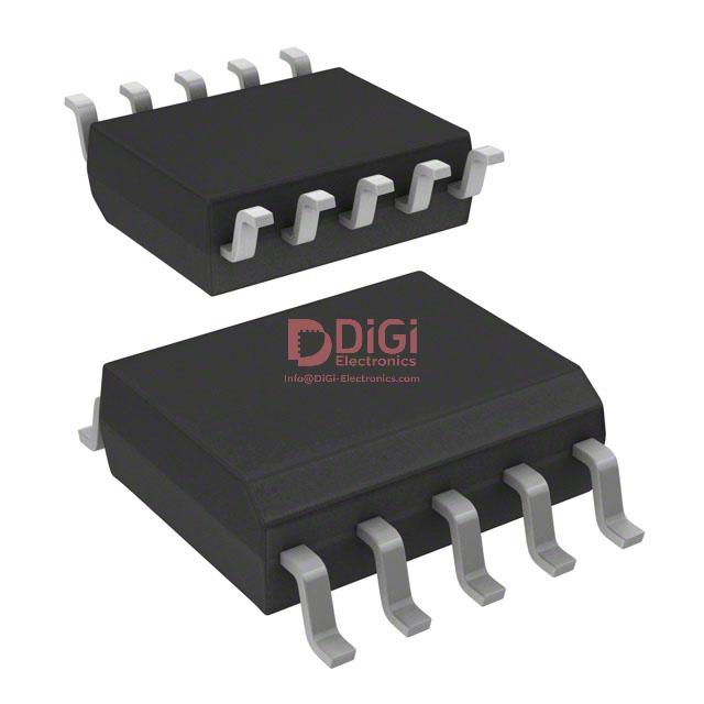
Package details and layout considerations for VIPER122LSTR
The VIPER122LSTR utilizes the SSOP10 package, a compact option engineered for high-density PCB layouts without sacrificing thermal management or electrical performance. This package selection strikes a precise equilibrium between footprint and power dissipation, accommodating applications that demand stringent space constraints and reliable heat dispersal. The pin pitch and body dimensions underpin dense routing possibilities, allowing signal and power paths to be optimized while minimizing parasitic effects that can impede high-frequency switching.
Analyzing the mechanical specifications provided by the manufacturer reveals that correct footprint design is critical for thermal and electrical robustness. Attention must be given to pad sizing and spacing, as these influence solder joint reliability and thermal conduction away from the package. The integration of thermal reliefs into the copper layout can further enhance heat flow, preventing hotspots during prolonged operation or elevated load conditions. Experience in board assembly demonstrates that a meticulously matched pad geometry reduces the risk of cold solder joints and promotes consistent reflow processes, minimizing field failures associated with poor mechanical bonds.
Thermal performance remains a central concern, especially in power electronics. The SSOP10 package offers a favorable surface-area-to-volume ratio, enabling effective heat exchange when combined with properly designed copper pours and thermal vias beneath and around the package. In practice, leveraging large ground planes not only bolsters heat dissipation but also enhances electrical noise immunity, vital for sensitive applications like switch-mode power supplies.
For projects demanding compliance with environmental standards, the ECOPACK®-compliant VIPER122LSTR simplifies adherence to global directives, notably lead-free and RoHS requirements. This characteristic addresses evolving industry mandates without necessitating design concessions, preserving longevity and supply chain resilience. The design process can thus prioritize performance and manufacturability without added compromise for regulatory conformity.
A nuanced perspective highlights that the synergy between package selection and PCB design directly dictates long-term reliability, manufacturability, and regulatory acceptance. Employing SSOP10 in conjunction with manufacturer-recommended footprint dimensions leverages industry best practices, promoting product consistency across high-volume production runs. The VIPER122LSTR stands as a refined solution for environments where miniaturization, thermal management, and compliance intersect, supporting scalable deployment in both consumer and industrial segments.
Potential equivalent/replacement models for VIPER122LSTR
When selecting an equivalent or replacement for the VIPER122LSTR, the engineering process pivots around a precise set of device parameters. Primary considerations should center on voltage rating consistency, with special attention to MOSFET avalanche energy capability, as substitution failures here can induce catastrophic damage, particularly in high-frequency switching environments. Integrated PWM control structures must be scrutinized for functional parity; variations in modulation technique or control strategy can incur deviations in output regulation, transient response, and EMI performance across varying load profiles.
Evaluating standby power characteristics is imperative, especially where regulatory compliance around no-load or low-load power draw is enforced. Devices exhibiting low quiescent consumption often employ advanced burst and skip-cycle operation, so not only must the datasheet values align, but application testing must validate that the alternate device achieves comparable energy savings during idle phases. Protection features require detailed cross-comparison—not just for the headline specifications, like overvoltage, overload, thermal, and short-circuit safeguards, but also for hidden implementation-specific behaviors, such as auto-restart timing, hiccup mode, and reset latching. Past project experience demonstrates that differences here can affect both field reliability and root-cause diagnosis for intermittent shutdowns.
Exploring the wider VIPER1xx family can yield streamlined integration by leveraging similar architectures and qualification data, reducing validation overhead for drop-in replacements. Specific variants may offer alternate package types or enhanced operational temperature ranges, optimizing board layout and reliability margins. However, transition to competitive offerings from established SMPS vendors requires a granular analysis beyond the headline specs; topology adaptability (buck, flyback, or boost modes), integrated start-up circuitry, and noise immunity must be assessed against the actual end application, as even minor deviations in switching characteristics can have cascading effects on system performance.
In practical deployment, supply voltage tolerance and transient immunity both materially impact robustness under brownout or surge conditions common in field installations. Efficiency metrics, especially under light-load and burst-mode scenarios, should be validated in-circuit, not just via datasheet review, as real-world variances often arise due to PCB parasitics, component selection, and thermal coupling. Prior experience with replacement models often reveals that subtle control algorithm differences can manifest as audible noise, excessive standby draw, or instability during crossover points.
Ultimately, effective second sourcing mandates a holistic understanding of both the electrical characteristics and the system-level integration touchpoints. Prioritizing underlying mechanisms—such as switching timing, protection circuit architecture, and PWM control philosophy—reduces the risk of undocumented incompatibilities. This layered analysis ensures not only continuity of supply but also operational reliability, minimizing the systemic risk introduced by alternate SMPS controllers or integrated flyback ICs.
Conclusion
The VIPER122LSTR from STMicroelectronics demonstrates a high level of integration in the realm of offline converter ICs, centering its architecture around a rugged 730 V avalanche-rugged power MOSFET. At the foundation, the device leverages advanced high-voltage technology and an efficient control core designed to fulfill stringent energy efficiency criteria without sacrificing robustness. Integrated start-up circuitry, current-mode PWM control, and sophisticated protection features—including overvoltage, overload, short-circuit, and thermal shutdown—collectively create a resilient barrier against common electrical stresses and system-level failures.
This comprehensive integration translates into tangible engineering advantages, particularly in board space minimization and BOM cost management. By substantially reducing the need for discrete external components such as start-up resistors, auxiliary winding circuitry, and complex snubber networks, the VIPER122LSTR streamlines PCB layout and supports automated assembly processes. Its ability to handle wide input voltage ranges and fluctuating line conditions also simplifies global certifications, a critical consideration as regulatory agencies escalate efficiency and durability demands on SMPS products.
Implementation experiences highlight the IC’s versatility across a spectrum of SMPS topologies, including auxiliary power rails for white goods, industrial modules, and smart home controllers. The notably consistent start-up performance and reduced thermal drift under variable load conditions directly contribute to longer system lifespans. Designers have reported that integrating the VIPER122LSTR significantly mitigates field returns attributed to component stress or improper sequencing, underscoring its impact on long-term operational reliability.
A key aspect revealed in practical projects is the acceleration of development cycles. Rapid prototyping is facilitated by ST’s well-documented reference designs, which exploit the VIPER122LSTR’s on-chip features to support robust EMI compliance and rapid fault recovery. The IC’s built-in burst mode operation and quasi-resonant management further address low standby power targets, aligning with global regulatory standards such as DOE Level VI or EU CoC Tier 2.
Analyzing ongoing trends, it becomes evident that the integration philosophy exemplified by the VIPER122LSTR represents a strategic inflection point for low- and mid-power SMPS design. By converging resilience and efficiency into a single package, this device encourages a holistic design mindset—prioritizing not only initial performance specs but also maintainability and total life-cycle value. Such an approach proves critical in differentiated product lines, where design agility and field reliability directly impact competitive positioning in energy-conscious markets.


