>
>


Product overview: Sharp PC814XJ0000F series optoisolator
The PC814XJ0000F optoisolator leverages an integrated infrared emitting diode (IRED) and a highly sensitive phototransistor, encapsulated within a durable 4-pin DIP form factor. This architecture exploits optical coupling, severing the direct electrical connection between the input and output sides. Such galvanic isolation is engineered to withstand input-output isolation voltages up to 5000Vrms, making this device indispensable for systems requiring robust separation of grounds or high-voltage domains.
Underpinning operation is the principle of photonic transmission: input signals energize the IRED, which emits infrared light proportional to drive current. The adjacent phototransistor responds to this optical stimulus, toggling its conduction state and recreating the input signal at the output. The efficacy of this mechanism ensures minimal propagation delay and enables reliable signal fidelity even in harsh electrical environments. Transistor output topology further improves compatibility, facilitating easy interfacing with standard analog and digital logic circuits.
In practice, the optoisolator demonstrates resilience against transients and common-mode voltage spikes that routinely challenge industrial control systems and communication backplanes. Applications routinely integrate the PC814XJ0000F series within microcontroller I/O expansion, industrial PLCs, and inverter gate drives, where suppression of ground loops is paramount. Intelligent placement within PCB layouts—such as positioning the optoisolator between domains with disparate logic levels—mitigates crosstalk and systematic noise, thereby elevating overall system integrity.
The device’s high voltage isolation threshold and compact package enable reliable deployment in densely populated electronic assemblies. Experience reveals that employing the optoisolator in fail-safe triggers and sensors not only reduces the risk of catastrophic coupling faults but also enhances system diagnostic accuracy by filtering transient anomalies at crucial isolation boundaries. Optimized biasing of the input current further tailors the response speed, allowing adaptation to high-frequency switching or precision low-speed signal transmission across diverse application spectrums.
A nuanced insight emerges from balancing isolation performance with circuit complexity: while the device’s simplicity accelerates implementation, subtle adjustments in the interface circuit—such as resistive loading at the phototransistor collector—result in improved linearity and wider bandwidth. Such refinements empower engineers to scale solutions from concise logic-level interconnects to complex, multi-channel feedback loops without compromising safety or electromagnetic compatibility. This layered approach consolidates isolation, control, and reliability, positioning the PC814XJ0000F series as a foundational element in resilient electronic design.
Key features and electrical characteristics of the PC814XJ0000F series
The PC814XJ0000F series introduces a blend of robust design and advanced electrical characteristics, precisely targeted for diverse PCB integration scenarios where both reliability and insulation are critical. Engineered in a compact 4-pin DIP package and an SMT gullwing variant, the component adapts efficiently to either through-hole or surface-mount assembly. The double transfer mold construction directly addresses process robustness, enabling high-yield flow soldering while minimizing the ingress of contaminants and moisture that often compromise optoelectronic reliability over extended operational cycles. This construction is a central factor in achieving consistent device performance, particularly in environments characterized by temperature cycling and flux-laden atmospheres.
The electrical architecture centers on an optically isolated phototransistor, tailored for AC input compatibility. This expands deployment versatility, especially in applications interfacing with both AC signal detection and microcontroller-level logic. Integral to the design is the high collector-emitter voltage rating of 80V, which secures operational margins when used in low-voltage monitoring circuits exposed to occasional voltage transients. Practical experience indicates this capability is particularly advantageous in industrial control panels and power line interface modules, where unpredictable voltage excursions are commonplace.
The device delivers a Current Transfer Ratio (CTR) spectrum of 20% (min.) to 300% within the defined input current of ±1mA, permitting flexible selection based on drive power and output loading requirements. This CTR breadth supports adaptation in signal conversion topologies, optoisolated feedback paths in power supplies, and error detection circuits. A nuanced aspect in implementation is the careful balancing of input drive current versus CTR, ensuring signal fidelity and timing margins are maintained—valuable when interfacing to CMOS or TTL stages with varied impedance.
Superior input-output isolation, with a rated withstand voltage of 5.0kVrms, positions the device for use in systems governed by rigorous insulation standards, such as medical electronics and industrial automation. This level of isolation is sustained by both the intrinsic optical separation and the materials selection underlying the transfer mold construction. In practice, adherence to this isolation specification mitigates cross-domain failure risks, especially under sustained over-voltage stress or repeated electrical disturbances.
Conformity to RoHS regulations and lead-free material selection ensures that the PC814XJ0000F aligns with global environmental directives while simplifying logistics for multinational manufacturing flows. This harmonization fosters universal replacement capability in world markets without necessitating additional qualification steps for hazardous substances compliance.
From a systems engineering viewpoint, the series demonstrates the importance of anticipating both electrical transients and long-term board-level operation requirements. The combination of high electrical isolation, broad CTR range, and robust packaging represents a balancing of opposing design demands—high performance under stress conditions, yet manufacturability in automated, high-throughput environments. Such integration reflects an established preference for building insulation and reliability into the foundation of optocoupler selection, directly impacting downstream system MTBF and regulatory certification outcomes.
Agency approvals and compliance information for the PC814XJ0000F series
The PC814XJ0000F series integrates robust agency approvals and compliance credentials, ensuring readiness for international market requirements. The core compliance mechanisms derive from two primary agency certifications: UL1577 and VDE, which address isolation integrity and operational safety in optocoupler applications. UL1577 recognition (file No. E64380, as model PC814) confirms the device’s capability to withstand high-voltage isolation, which remains critical in safeguarding both equipment and users in systems handling hazardous voltages. This certification underscores the series’ alignment with stringent US standards for optical isolation, facilitating its use in critical path signal interfaces—particularly in industrial control boards, switch-mode power supplies, and systems with reinforced insulation demands.
VDE approval (DIN EN60747-5-2, file No. 40008087, as model PC814) adds a complementary layer of assurance aligned with European directives. As a direct successor to DIN VDE0884, this certification verifies conformance to advanced optoelectronic component standards, focusing on insulation coordination and long-term reliability. Selection of the VDE-approved variant becomes prudent in scenarios where system architecture mandates cross-continental interoperability—such as distributed automation networks, motor drives, or medical diagnostic platforms. When integrating these components, explicit referencing of VDE files in technical documentation can expedite both internal design validation and external system audits.
Beyond electrical safety, material compliance directly enhances system resilience. The PC814XJ0000F’s package resin meets UL 94V-0 flammability classification. This attribute is indispensable where thermal events, abnormal overloads, or board-level faults could expose components to ignition risks. Consistent flame retardance across batches limits propagation potential, aligning with both safety-critical product mapping and the evolving regulatory landscape of functional safety.
A nuanced understanding of how these certifications coalesce in real-world design improves project outcomes. Early selection of components with dual US and EU approvals streamlines procurement for multinational production, minimizes certification reruns, and supports rapid platform customization. In practice, design cycles benefit when optocoupler agency file references are embedded in compliance matrices and procurement tools. This strategy mitigates late-stage design pivots caused by overlooked regional specifications.
Observing current market trends, there is increasing emphasis on verifiable documentation throughout the supply chain. Products conforming to both agency isolation and flame-resistance benchmarks simplify not only regulatory submissions but also enhance confidence during high-power board troubleshooting or on-site technical audits. Integrating the PC814XJ0000F series facilitates resilience at the system level, leveraging global certifications to address both operational integrity and deployment agility.
Application scenarios and integration considerations for the PC814XJ0000F series
The PC814XJ0000F series optocouplers are strategically incorporated into control logic stages for programmable controllers, telecommunication systems such as telephone sets and exchanges, and automation-centric appliances. Their dielectric isolation serves as a critical interface, translating electronic signals across circuits characterized by disparate potentials or impedance. This high-voltage insulation sharply reduces risks of cross-talk and transient coupling, safeguarding sensitive digital subsystems.
At a design level, two properties underpin their adaptability: AC input compatibility and a broad Current Transfer Ratio (CTR) spectrum. The AC input tolerance allows designers to interface bidirectional signals without additional rectification stages, simplifying layouts especially in switching architectures and relay driving circuits. The flexible CTR enables precise matching between input drive levels and output response, accommodating various logic families and load requirements. For industrial automation panels, this flexibility permits tight clustering of control channels with reliable isolation, while the wide operating current capability streamlines integration with PLC input modules—minimizing component spread and PCB area.
Attention to circuit footprint and thermal management is vital; the PC814XJ0000F series exhibits predictable thermal behavior under full load, which helps prevent drift and degradation over extended operating cycles. Integrating the device into signal chains that require waveform integrity across high common-mode voltages reveals consistent switching thresholds. In large-scale deployments, such as distributed telecommunication exchanges, the optocoupler’s robust isolation withstands ground potential differentials and electromagnetic interference, maintaining channel fidelity and uptime. One effective approach for enhancing noise immunity is to pair PC814XJ0000F units with low-pass filters at their inputs, which attenuates unwanted high-frequency disturbances in office automation systems.
A nuanced aspect of deploying this series lies in managing the trade-off between CTR spread and propagation delay. Selection of devices within the series for time-sensitive feedback loops in automated machinery directly improves response precision. Empirical evaluations show that using matched pairs of PC814XJ0000F optocouplers in redundant safety circuits enhances fault tolerance—mitigating risks associated with single-point isolation failure.
Design choices that integrate the PC814XJ0000F series not only satisfy the basic requirements of galvanic isolation but introduce scalable modularity, promoting rapid reconfiguration in evolving appliance frameworks. This positions the component as a core enabler for reliable, high-density control solutions in both legacy and next-generation automation systems.
Absolute maximum ratings and electro-optical performance data of the PC814XJ0000F series
Absolute maximum ratings form the primary limits governing safe operation of PC814XJ0000F series optocouplers. These ratings specify thresholds for parameters such as forward current, peak forward current, and reverse voltage at the input diode, alongside collector-emitter voltage, emitter-collector reverse voltage, collector power dissipation, and total power dissipation within the output transistor. The constraints derive from device physics: exceeding them initiates risks of irreversible junction damage, insulation breakdown, and accelerated aging, particularly as localized heating and electric field stress can induce early failure. In practice, design margin is introduced below these maxima; engineers apply derating factors based on empirical test data and failure mode analysis to bolster long-term reliability and minimize latent defects.
Delving into electro-optical parameters at a controlled ambient of Ta=25°C, current transfer ratio (CTR) stands out as a critical design variable, directly linking input-side drive current to output-side collector current. Temporal response characteristics—namely turn-on and turn-off times—define upper frequency boundaries for signal fidelity and switching speed. Forward voltage, typically 1.2V–1.4V for the input diode, impacts control logic compatibility, while collector dark current quantifies leakage paths and their influence on quiescent states. Well-characterized response times are essential for systems interfacing with microcontrollers or high-speed digital buses; limited bandwidth not only restricts speed but may also introduce jitter and timing uncertainty in edge-triggered circuits.
Real-world integration strategies emphasize the interplay between absolute ratings and operational electro-optical characteristics. Board-level experience reveals that the performance envelope of PC814XJ0000F devices can shift with layout parasitics, temperature drift, and input waveform fidelity. For instance, overshooting input current—even for microseconds—can precipitate CTR degradation or premature optoelement fatigue. In high-density environments, power dissipation constraints accentuate the need to model thermal gradients across the device footprint, ensuring collector heating remains subdued, thus preventing cumulative stress. Selecting bias resistors and voltage clamps with consideration of voltage rating margins remains crucial for error-free switching across industrial control or instrumentation contexts.
Architecturally, the strength of PC814XJ0000F emerges in its balance of isolation voltage, operational bandwidth, and CTR stability. The internal structure—optical coupling via precision LED-phototransistor alignment—allows robust galvanic separation, a property pivotally shaped by adherence to absolute maximums and optimized by exploiting the device’s response time for real-time multiplexed data links. A nuanced approach leverages systematic temperature characterization and extended reliability testing, extracting maximal performance without encroaching upon threshold boundaries.
From the perspective of system design, optimal deployment entails judicious parameter mapping. Using manufacturer-provided characteristic curves, one can predict device behavior under fluctuating input conditions and supply noise profiles. This supports proactive component selection and PCB routing modifications to refine EMI immunity and transient response. Such layered engagement—from semiconductor physics underpinning rating limits to board-level power budgeting and application-specific validation—ultimately anchors both enduring safety and high-performance operation in precision optocoupler design.
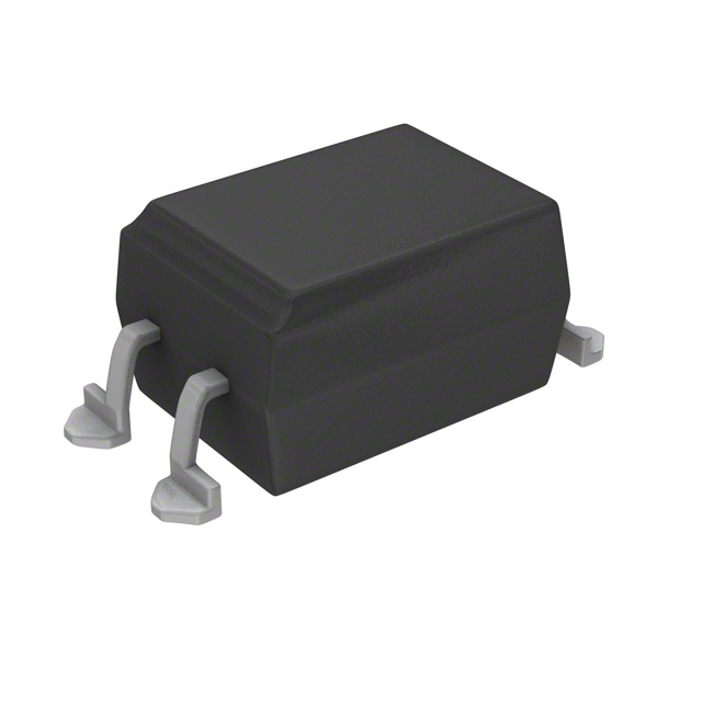
Mechanical layout and pin configuration of the PC814XJ0000F series
The PC814XJ0000F series optocoupler demonstrates a compact and robust mechanical layout, specifically structured to optimize both automated and manual insertion during PCB assembly. The dual-in-line package not only facilitates straightforward orientation but also minimizes potential alignment errors, a key consideration in high-density board designs where tolerance for deviation is minimal. Structural rigidity is achieved through well-selected molding compounds and termination finishes, crucial for maintaining package integrity during thermal cycling or mechanical stress encountered in mass soldering processes.
Pin configuration adheres to a logical sequence enhancing both user comprehension and circuit trace routing efficiency. Pins 1 and 2 function as the input side, representing the anode and cathode of the internal light-emitting diode, with the ability to accommodate standard polarity conventions depending on circuit requirements. Pins 3 and 4 serve as the output interface, acting as emitter and collector terminals of the integrated phototransistor. This arrangement isolates the control and load circuits electrically, a fundamental mechanism underpinning the device’s utility in noise-sensitive or high-voltage domains. In practice, the clear segregation between input and output paths prevents inadvertent miswiring, reducing nonfunctional solder joints and associated rework costs.
Material selection, such as SnCu lead plating, plays a nontrivial role in solder joint reliability and long-term corrosion resistance. The tin-copper alloy plating demonstrates superior wettability and mechanical bonding during reflow or wave soldering, enabling high-yield board assembly even under varied surface-mount profiles. This finishing choice also aligns with lead-free compliance standards, supporting integration into global production pipelines without necessitating specific process modifications.
Outline dimensions are precisely standardized, ensuring seamless fit within automated pick-and-place vision systems and simplifying stencil aperture alignment for reliable solder paste deposition. Consistent form factors across the PC814XJ0000F series reduce the need for multiple unique footprints, streamlining both PCB design and inventory management. Practical experience reveals that such uniformity leads to lower error rates and reduced cycle times in multi-variant product lines, especially when scaling up from prototype to full production.
A disciplined approach to mechanical and pin layout, as seen in the PC814XJ0000F optocoupler series, directly translates to measurable improvements in system reliability and manufacturability. By implicitly addressing typical assembly challenges and compliance constraints, this design philosophy enhances versatility and accelerates integration cycles in both legacy and emerging application scenarios.
Design considerations and reliability notes for the PC814XJ0000F series
When evaluating the PC814XJ0000F series for circuit integration, the following factors merit targeted scrutiny from an engineering perspective. At the core lies the current transfer ratio (CTR), which exhibits pronounced nonlinearity at low input current levels, specifically when the forward current (I_F) drops below 1 mA. This behavior is typical for non-coherent IRED-based optocouplers but warrants special attention during signal conditioning and threshold design. Analog signal applications, low-power microcontroller interfacing, or high-impedance sensor readout frequently risk error margins under-represented by standard CTR curves unless characterized across the full expected operating input current range.
Deeper analysis reveals aging mechanisms that compromise transfer efficiency over time. The integral infrared emitter diode inside the PC814XJ0000F is prone to gradual photonic degradation, a well-documented phenomenon in GaAs-based emitters subjected to continuous bias. Long-term performance benchmarks suggest up to a 50% reduction in radiant intensity and CTR during five years of uninterrupted service. This temporal shift mandates forward-thinking derating protocols and parametric guard bands during system qualification; failure to adapt circuit thresholds or refresh calibration intervals can introduce latent faults. Especially in demanding contexts—such as power railway interlocks, industrial fail-safes, or remote telemetry modules where infrequent maintenance prevails—the design envelope must absorb operational drift with margin, automated CTR recalibration, or even engineered redundancy.
Environmental deployment further demarcates the PC814XJ0000F platform. The absence of internal coherence within the IRED precludes its suitability for irradiation or radiation-hardened scenarios. Even moderate gamma or neutron exposure can induce transient or permanent loss of functionality, thus direct substitution into medical imaging electronics, spaceborne modules, or nuclear facility feedback loops is contraindicated. Experience underscores that ensuring stable isolation and signal fidelity in these installations generally demands optocouplers engineered with coherent emitters and certified for irradiation resilience.
Layering these engineering insights facilitates robust realization strategies. Circuit designers often accelerate reliability testing, cycling units across variable I_F and ambient temperature profiles to empirically map CTR variance and anticipate population-level device spread. Integration patterns favor configuration with pre-emphasis on input current stabilization—using precision current sources, adequate pull-up/pull-down resistors, or active feedback loops—to maintain CTR within optimal boundaries, extending both observable dynamic range and effective device lifespan. Notably, systems tasked with safeguarding critical actuation or monitoring require auxiliary calibration logic, capable of periodic in-situ CTR characterization, paired with firmware routines that adapt to measured optocoupler drift. These defensive architectures, informed by predictive maintenance paradigms, outperform static designs and bolster reliability without incurring prohibitive complexity.
A nuanced approach to integrating the PC814XJ0000F series thus synthesizes foundational knowledge of emitter physics, real-world degradation models, and the risk landscape of target deployment environments. Matching component limitations with resilient electrical topologies and forward-defined maintenance schedules leverages the device’s strengths while safeguarding against common pitfalls. Ultimately, system resilience in the face of evolving CTR and emitter aging is achieved not through reactive mitigation, but via the strategic, layered incorporation of predictive engineering practices.
Manufacturing guidelines for assembly of the PC814XJ0000F series
Adhering to precise manufacturing protocols in the assembly of the PC814XJ0000F series optocouplers is critical for ensuring long-term reliability and consistent isolation characteristics. Soldering procedures must observe optimized thermal profiles to prevent thermal stress-induced degradation of internal components, especially the LED and phototransistor interface. Reflow soldering demands strict compliance with the outlined temperature gradient; exceeding two cycles introduces risk of microfractures within the encapsulant, compromising optical coupling efficiency. In practical deployment, close monitoring of temperature ramp rates and dwell times prevents latent defects from propagating throughout production batches.
For flow soldering, the established maximum of 270°C for a duration under ten seconds, coupled with controlled preheat between 100°C and 150°C for 30 to 80 seconds, minimizes risk of substrate warping and dielectric breakdown. Empirical data suggest that narrow control of these windows reduces instances of solder bridging and preserves lead integrity, which proves especially significant in automated high-density board assemblies. Techniques such as targeted thermal profiling using thermocouples and infrared mapping facilitate early detection and mitigation of temperature overshoot, which otherwise may go unnoticed until post-assembly testing.
Hand soldering, although less prevalent in scaled manufacturing, finds its place in repair and prototyping scenarios. The stipulation to remain below 400°C and limit contact to three seconds mitigates localized thermal shock on the device package. Operators benefit from tip temperature calibration and employing heat sinks during critical operations, exposing a nuanced layer to process control often overlooked in bulk production environments. Consistent adoption of these measures typically results in measurable improvement in input-output voltage withstand margins during isolation tests.
After soldering, contamination control is paramount. Solvent cleaning under 45°C for up to three minutes is recommended, with solvents such as ethyl, methyl, or isopropyl alcohol promoting effective flux residue removal without attacking the package resin or internal wire bonds. When ultrasonic cleaning is under consideration, a tailored assessment—factoring frequency, solvent chemistry, and immersion time—is essential to avoid cavitation stress on delicate bond wires and encapsulant surfaces. Experience reveals that precisely modulated ultrasonic parameters preserve device isolation while ensuring removal of residues that could compromise dielectric strength on conformal coating applications.
The overarching insight is that assembly discipline—coupled with thorough cleaning strategies—directly impacts isolation integrity, device lifespan, and field reliability metrics. The layered approach to thermal management and contamination control serves as a blueprint for achieving repeatable yields and mitigating post-assembly failures, particularly in high-isolation requirements typical of power management and control circuits. Deploying these measures as standard practice not only aligns with datasheet guidelines but advances baseline manufacturing quality across product lines.
Environmental and regulatory compliance of the PC814XJ0000F series
The PC814XJ0000F series integrates proactive strategies to address both environmental and regulatory mandates, structured around strict adherence to international frameworks. At a material selection level, the absence of ozone-depleting substances and restriction of RoHS-listed elements—lead, mercury, and hexavalent chromium—form the foundation for its compliance profile. The systematic elimination of flame retardants including polybrominated biphenyls (PBB) and polybrominated diphenyl ethers (PBDE) reflects a nuanced understanding of evolving directives, notably those issued by the European Union and extensions implemented globally.
Manufacturing processes for this series prioritize closed-loop supply verification, ensuring that upstream sourcing aligns with hazardous substance control. Continuous batch analysis and third-party conformity assessment fortify reliability, a critical factor for designers and integrators facing varied regulatory environments. The operational traceability embedded within the procurement and assembly stages minimizes the risk of non-compliance at the field application level.
From an integration perspective, selection of the PC814XJ0000F series offers assurance against potential legal liabilities and reputational risks connected to environmental infractions. Real-world deployment often demands material declaration and end-of-life management; by defining clear exclusion of persistent toxicants, this series facilitates straightforward documentation and recycling pathways. Such design choices support streamlined qualification for eco-labeling and sustainable procurement initiatives without extensive re-validation.
Close attention to legislative trajectory is evident in the product’s specification: anticipation of shifts, such as REACH extensions or regional regulatory updates, prevents obsolescence and supports long-term robustness for high-volume OEM deployment. The conservative approach to chemical risk not only meets explicit directives but often exceeds minimum thresholds, yielding a margin of safety for future adoption as protocols evolve.
Strategically, embedding compliance within core material formulations sets a precedent for more agile engineering across platforms. The PC814XJ0000F series demonstrates that forward-thinking design, anchored in regulatory intelligence and clean manufacturing, functions as both a technical advantage and a risk mitigation tool in contemporary electronic systems.
Packaging specifications and logistics for the PC814XJ0000F series
The PC814XJ0000F series offers two primary packaging solutions optimized for both manual and automated assembly requirements: sleeve packaging and tape-and-reel. The sleeve option leverages anti-static high-impact polystyrene (HIPS), effectively minimizing electrostatic discharge risk during handling and storage—an essential consideration to preserve sensitive optoelectronic integrity and reduce device failure rates before PCB mounting. Each sleeve accommodates up to 100 units, supporting smaller-scale manufacturing environments that may prioritize inventory agility over raw throughput. This format proves advantageous in prototyping scenarios or where line changeovers are frequent, as the manageable batch size aligns well with varying production needs.
Tape-and-reel packaging extends the series’ suitability for high-volume, automated SMT (Surface-Mount Technology) operations. By integrating polystyrene (PS) carrier tape with a polyethylene terephthalate (PET) cover tape, this solution enhances component protection against physical and ESD damage during transit through automated feeders and pick-and-place machinery. Each reel's 2,000-piece capacity aligns with industry-standard tape widths and pitch tolerances, facilitating predictable supply intervals and minimal downtime—a decisive factor for continuous production. The anti-static properties of both the carrier and cover materials further dampen electrostatic discharge, ensuring stable device quality during mass placement cycles.
Transitioning between packaging formats is seamless due to dimensionally consistent housings and standardized lead configurations. This eliminates the need for feeder recalibration or container modifications, streamlining the workflow from storage to mounting station. When implemented in high-throughput facilities, tape-and-reel packaging can significantly boost placement rates by reducing replenishment events and aligning with automatic loader mechanisms. Conversely, the sleeve option offers a tactical advantage where production runs must remain flexible or where inventory traceability per package is prioritized.
Underlying these packaging strategies is the imperative to minimize device handling steps, thus inherently reducing process-induced risks. In field applications, adopting the optimal packaging format directly impacts both yield and operational uptime. Overlapping logistical considerations—such as package stackability, weight distribution, and labeling standardization—contribute further efficiency gains through ease of transport and warehouse management.
A nuanced observation is that well-engineered packaging extends beyond protection: it forms a bridge between component reliability and the demands of contemporary manufacturing strategies. Investing in packaging configurations that anticipate downstream process needs can yield disproportionately large productivity benefits, especially as assembly lines evolve toward greater automation and traceability. This layered, application-driven approach to packaging selection underpins both the short-term efficiency of device installation and the long-term durability of the end product.
Potential equivalent/replacement models for the PC814XJ0000F series
Evaluating alternatives to the PC814XJ0000F series requires a systematic approach focusing on key optoisolator parameters and practical integration concerns. The PC844XJ0000F series, engineered in a 4-channel configuration, establishes a robust foundation for multi-channel isolation, streamlining board layout and reducing component count in densely populated circuits. This model retains core optoelectronic characteristics—such as input-output isolation, current transfer ratio (CTR) consistency, and response time—that closely align with PC814XJ0000F, supporting direct substitution in applications where channel scalability and board space efficiency hold priority.
A granular assessment involves examining isolation voltage ratings to maintain system integrity under transient faults and signal surges. The PC844 series exhibits comparable insulation strength, with design validation often confirming conformance to safety regulatory standards like UL and VDE. Thorough attention to CTR—the ratio of output current to input—ensures output fidelity and timing within signal-coupled subsystems, particularly relevant in programmable logic, motor control, and industrial automation domains. Variations in CTR across optoisolator series can create subtle behavioral differences in output activation; precise model selection mitigates these effects.
Packaging dimensions and pinout convention become critical in retrofit or upgrade scenarios. The PC844XJ0000F, offering a DIP package consistent with common PCB footprints, simplifies direct replacement without redesign. Pin assignments and form factor should be cross-referenced against project documentation to minimize implementation risk. Beyond physical attributes, agency certifications underpin regulatory compliance, especially in designs destined for safety-critical environments. Optoisolators validated under recognized standards accelerate approval cycles and reduce liability—an often underestimated factor during development sprints.
Experience with large-scale deployments demonstrates that multi-channel devices, like the PC844, are advantageous in series signal isolation—reducing electromagnetic interference and enabling tighter coupling between control and sensing electronics. Integrating such devices supports modular design philosophies and system maintainability, while variations in CTR and isolation ratings influence fault tolerance strategies. Advanced projects benefit from explicit attention to datasheet nuances, particularly absolute maximum ratings and recommended operating conditions, preventing latent reliability issues.
Critically, a nuanced approach to model selection leverages both electrical parameters and practical deployment data. Optoisolator replacements must strike a balance between seamless physical fit, electrical compatibility, and safety validation, with the multi-channel PC844 series serving as a valuable alternative for architectures seeking greater isolation density and simplified assembly. Discerning engineers exploit cross-series substitution patterns to optimize cost, assembly complexity, and long-term reliability.
Conclusion
The Sharp PC814XJ0000F series embodies a strategically engineered optoisolator solution optimized for high-reliability environments. At the architectural level, it leverages robust phototransistor output with galvanic isolation, ensuring critical signal integrity across high-voltage boundaries. The insulation distance and resultant isolation voltage ratings address stringent safety requirements inherent to industrial automation, smart grid infrastructure, and telecom system boards, where transient voltage and noise immunity are core design considerations.
A key strength lies in the device's flexible current transfer ratio (CTR) specification, maintained across a broad temperature range and input LED currents. This characteristic aids circuit designers in achieving predictable system response without frequent requalification, particularly in multi-sourced or upgradable platforms. In practice, careful matching of CTR to input logic thresholds reduces component derating, which simplifies both initial validation and ongoing product evolution.
Regulatory compliance, including international safety approvals, accelerates time-to-market for final assemblies and supports easier certification efforts. The optoisolator's compliance profile, combined with documented reliability data derived from life testing and accelerated stress scenarios, underpins its use in mission-critical control loops and input isolation for microcontroller-based circuits or sensor interfaces. Its reliable plastic dual in-line package (DIP) footprint is compatible with automated assembly and reflow soldering, promoting efficient, defect-minimized production at scale.
Proactively, selection of the PC814XJ0000F series addresses long-term supply chain stability and reduces variability in maintenance operations, given its multi-sourced availability and backward-compatible pinout. The performance and documentation ecosystem—application notes, SPICE models, and prolonged vendor support—fosters rapid design, simulation, and troubleshooting during both prototyping and field maintenance cycles.
In synthesis, the engineering value of the PC814XJ0000F series lies in its seamless blend of robust safety, steady performance consistency, and ease of adoption in diverse applications. The approach to optoisolator design as a system-level enabler, rather than a simple isolation component, yields tangible benefits in functional safety, system longevity, and manufacturing scalability—elements that define modern electronics procurement and design excellence.