>
>


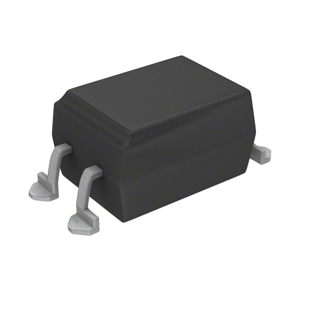
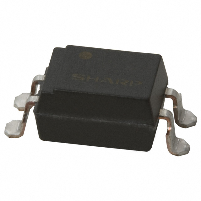
Product overview: PC3Q510NIP Sharp Microelectronics optoisolator
The PC3Q510NIP from Sharp Microelectronics exemplifies advanced optoisolator design, integrating four independent isolation channels within a compact 16-pin Mini-flat package. This architecture directly addresses the high-density requirements of modern control and signal-processing systems, where board real estate is at a premium and multi-channel isolation is a recurring challenge. By embedding four channels in a single device, the PC3Q510NIP not only simplifies PCB layout but also improves system reliability by reducing interconnect complexity and potential points of failure.
At its core, the device utilizes light-emitting diodes (LEDs) and corresponding photodetectors to realize galvanic separation between input and output circuits. The signal is transferred as light across an insulating gap, completely decoupling the electrical paths. This mechanism is fundamental in safely interfacing control logic, such as microcontrollers or FPGAs, with high-voltage or noisy subsystems. The absence of direct electrical contact mitigates risks associated with ground potential differences, surges, and electrical transients, essential for compliance with safety standards like IEC 61010 or UL 1577.
Engineering applications often drive the selection of the PC3Q510NIP over discrete solutions. Industrial motor drives, for example, routinely implement such quad-channel optoisolators to transmit feedback signals from high-voltage domains to low-voltage logic safely and efficiently. In telecom base stations, compact multi-channel isolation supports rapid signal level translation while maintaining stringent isolation barriers vital to network reliability.
The PC3Q510NIP’s Mini-flat package further enhances thermal performance by ensuring a short heat path from active elements to PCB copper planes. This is especially notable in applications with elevated ambient temperatures or high duty-cycle operation, where long-term reliability hinges on efficient heat dissipation. Real-world integration often reveals that optimized footprint and lead configuration simplify automated assembly, reducing production defects associated with manual placement or wave soldering.
Notably, optoisolator selection impacts both functional safety and EMC robustness. Device parameters such as the isolation voltage, common-mode transient immunity, and input forward current thresholds must align with system-level requirements. The PC3Q510NIP’s specification supports robust insulation ratings, making it suitable for circuits exposed to fault conditions or repeated switching events. Design insights show that placing optoisolators early in the signal path maximizes noise immunity and minimizes crosstalk, especially in fast-switching environments.
The advancement embodied in the PC3Q510NIP demonstrates a subtle trend in industrial component design: consolidation of function and safety within standard packages. This approach fosters consistency across product platforms and shortens development cycles, a critical factor in competitive sectors. Selecting such multi-channel optoisolators enables scalable designs, where expanding input/output counts does not proportionally increase board area or isolation complexity. Deployment in automation panels and remote telemetry units underscores the importance of reliable optical isolation in maintaining uninterrupted signal flow and system diagnostics across diverse operating conditions.
In summary, the PC3Q510NIP serves as a robust building block for electronically isolated signaling, merging high-density integration with proven optoelectronic isolation principles. Its careful alignment with the mechanical, thermal, and safety demands of industrial, telecom, and automation contexts marks it as an optimal solution for next-generation control architectures where space and isolation are equally paramount.
Key features and technical specifications of the PC3Q510NIP
The PC3Q510NIP integrates advanced optoelectronic isolation technology with a form factor optimized for high-density PCB layouts. At its core, the device incorporates four optically isolated channels, built within a compact “Mini-flat” half-pitch package. The 1.27 mm lead pitch not only conserves board space but also facilitates straightforward routing in multilayer designs—a strategic advantage in control modules and communication interfaces where isolation and miniaturization are equally critical.
Key mechanical and assembly considerations are addressed by the adoption of a double transfer mold package. This structurally robust encapsulation offers enhanced reliability against moisture ingress and mechanical stress, ensuring consistent optoisolator performance across harsh industrial environments. Compatibility with standard flow soldering processes simplifies assembly line integration, reducing overall production costs and minimizing thermal exposure that could undermine isolation barriers.
The input stage stands out through its low forward current requirement, operating reliably with as little as 0.5 mA. This reduction in drive current has system-wide implications: microcontroller and logic outputs can directly control the device without external pre-drive circuitry, streamlining designs and preserving I/O power budgets—an important consideration in distributed automated systems and battery-sensitive applications.
The phototransistor output stage adopts a Darlington configuration, significantly amplifying the input signal. This results in a minimum current transfer ratio (CTR) of 600% at a mere 0.5 mA input, ensuring robust signal integrity even when only weak drive currents are available. The Darlington topology’s high gain extends application versatility into signal monitoring, PLC inputs, and digital interfacing where long wiring or parallel inputs would otherwise risk signal degradation.
A critical safety parameter—the input-to-output isolation voltage—is rated at 2.5 kVrms. This high level of galvanic isolation provides robust protection against overvoltages, transients, and ground potential differences, thereby safeguarding low-voltage logic domains from disruptive or hazardous events on the load side. Such isolation capability is indispensable in inverter boards, industrial automation controllers, and remote sensor nodes, where electrical separation is mandated by regulatory requirements or risk management guidelines.
Material selection reflects disciplined attention to safety and compliance. The inclusion of UL94V-0 flame-retardant package resin and recognition under UL1577 for double protection isolation positions the PC3Q510NIP as an optimal solution for systems requiring certified isolators. These credentials foster confidence in adoption for mission-critical designs, reducing the burden of external certification and accelerating time-to-market for end products.
Real-world deployment of the PC3Q510NIP demonstrates its strengths in compact motor drives, networked power management modules, and high-performance signal conditioning blocks. Its isolation resilience dramatically reduces signal cross-talk in dense PCBs, while the low input current capability simplifies expansion across multi-channel arrays. As thermal budgets tighten and layout constraints increase, devices embodying this combination of electrical strength, compactness, and assembly efficiency distinctly outperform legacy optoisolators.
Modern circuit design increasingly prioritizes holistic integration: the PC3Q510NIP exemplifies this trend by balancing isolation, efficiency, and manufacturability. Ultimately, leveraging such components supports system scalability, simplifies safety compliance, and directly contributes to robust, space-saving electronic architectures—a direction that defines contemporary industrial and commercial electronics.
Internal structure and packaging details of the PC3Q510NIP
Visible beneath the encapsulation of the PC3Q510NIP are four discrete opto-isolator channels, each comprising a matched pair of high efficiency IREDs and Darlington-coupled phototransistors. This configuration sharply elevates current transfer ratio (CTR), particularly under low input drive conditions, by leveraging both the inherent sensitivity gain and the compounding amplification characteristic of Darlington stages. The arrangement is engineered for optimal input-output isolation, permitting reliable signal transmission between circuits while robustly attenuating ground loops and transient-induced interference.
The pairwise alignment of the IREDs and phototransistors within each channel is precisely controlled during die placement to maximize radiative coupling efficiency, a critical factor in maintaining repeatable optical performance across production batches. Electrical isolation is further reinforced by the wide creepage and clearance distances inherent to the device’s internal layout. The spatial separation of signal paths mitigates cross-channel interference, enabling safe operation in high-density mixed voltage environments.
Encapsulation utilizes a double transfer mold technique, producing a homogenous mechanical barrier around the entire die assembly. This manufacturing approach confers substantial resistance to thermal shock and reflow soldering stress, characteristics consistently validated during high-volume SMT placement and IR oven profiling. The result is low package warpage and stable mechanical integrity without sacrificing optical transparency or interface reliability.
The half-pitch Mini-flat form factor addresses contemporary requirements for board miniaturization and high channel density. The slender package, weighing only 0.3g, interfaces seamlessly with high-speed pick-and-place systems, while its standardized outline and lead spacing facilitate straightforward PCB routing—critical in multi-channel designs for industrial automation, data acquisition, and medical instrumentation. Focused marking and pin identification, mapping anodes, cathodes, emitters, and collectors, eliminates assembly ambiguity and accelerates layout verification. This clarity translates to accelerated design cycles and improved first-pass yield during production ramp-up.
In practical deployment, maintaining uniform input drive across channels prevents CTR drift, particularly in temperature-fluctuating environments common to factory floors and embedded control units. When designing multi-channel interfaces on densely populated PCBs, leveraging the PC3Q510NIP’s explicit pin mapping can contribute to electromagnetic compatibility by enabling deterministic signal path routing. Integrating the optocoupler within feedback control loops or isolated sensor arrays exploits its high isolation voltage and low propagation delay, yielding tangible benefits in system reliability and data integrity.
A subtle but impactful advantage emerges from the synergy of its mechanical fortitude and optical precision: consistent long-term performance in environments prone to vibration, humidity, and thermal cycling. This reliability stems not only from the robust package but also from the layered optical and electrical isolation strategies embedded in the core design, offering enhanced lifecycle values and minimal maintenance requirements for mission-critical systems.
Application scenarios for the PC3Q510NIP optoisolator
The PC3Q510NIP optoisolator serves as a key component in engineered systems requiring robust signal isolation and enhanced electrical safety. Its architecture leverages an advanced phototransistor output coupled with optimized input sensitivity, resulting in high current transfer ratio (CTR) and minimal drive requirements on the signal side. This configuration enables efficient interfacing with low-power logic and sensor circuits, ensuring reliable state detection even in noisy environments.
In programmable logic controllers (PLCs), precise input/output segregation is critical for preventing signal contamination and maintaining deterministic operation. The PC3Q510NIP delivers strong galvanic isolation between control and field levels, suppressing transient surges and minimizing the risk of ground potential differences inducing false triggers. Multi-channel deployment streamlines modular expansion, allowing for systematic scaling of protected inputs without delay or excessive PCB real estate consumption.
Telecommunications infrastructure presents scenarios where channel-to-channel independence determines system resilience. Facsimile switching units and multi-line exchanges utilize the optoisolator's fast response and low propagation delay to transfer control pulses free of crosstalk and electromagnetic interference. The high CTR further reduces biasing complexity, promoting consistent switching thresholds across wide supply voltage ranges—vital for legacy systems and modern upgrades alike.
Automation and distributed control platforms confront recurring ground loop challenges, especially when interconnected machinery spans physical distances. Integrating the PC3Q510NIP in input protection networks addresses not only isolation but also transient suppression. Practical design approaches employ the optoisolator at signal boundaries adversely affected by line surges or field-generated spikes. Repeated deployments demonstrate that failures attributed to induced voltages diminish sharply with correct placement, improving uptime across diverse industrial scenarios.
The device’s ability to accommodate both digital pulse transmission and analog signal separation extends its usefulness beyond conventional relay alternatives. Configured in monitoring circuits, it interfaces with ADC inputs, isolating measurement domains from process control hardware. Benefits include reduction in offset errors and preservation of signal fidelity where high-speed acquisition is required.
One nuanced consideration involves optimizing CTR selection per channel to match system drive constraints, balancing sensitivity against noise immunity. Empirical tuning of input resistor networks in test assemblies repeatedly uncovers the critical threshold where overshoot is suppressed without sacrificing detection accuracy. This iterative adjustment is key to maintaining the optoisolator's operational margin under varying load and temperature profiles.
In summary, the PC3Q510NIP reveals itself as a versatile isolation solution in environments demanding precision, modular scalability, and integrity in data acquisition. Its multidimensional strengths—ranging from minimalistic interface requirements to superior transient tolerance—support deployment in both legacy retrofits and advanced automation endpoints, consolidating its position as a preferred choice for demanding isolation scenarios.
Engineering and design considerations for the PC3Q510NIP
When integrating the PC3Q510NIP photocoupler—an optically isolated device designed for signal transmission and basic switching—engineering focus must be directed toward both intrinsic characteristics and system-level ramifications. Accurate assessment of the underlying optoelectronic mechanisms is essential for robust circuit implementation, especially as device behavior can subtly shift under real-world operating conditions.
CTR (Current Transfer Ratio) variance represents a critical device parameter, heavily influenced by input drive conditions. At input currents below 0.5 mA, statistical dispersion in CTR increases due to non-linear photoemission and associated process tolerances, exposing receiving circuits to greater uncertainty. Designs that anticipate supply fluctuations or purposeful low-current control stimuli should compensate by incorporating wider tolerance margins or applying closed-loop feedback to stabilize output levels. Empirically, the most stable operation is achieved above this threshold, often dictating minimum drive requirements even in applications where energy efficiency is prioritized. For high-fidelity signal chain tasks—such as analog feedback paths or isolated serial communication—adhering to optimal input drive windows directly translates to lower error rates and improved immunity to drift.
Longevity is shaped primarily by internal infrared emitter diode (IRED) aging. Over typical five-year field deployments, output degradation can reach or exceed 50%, depending on on-time duty cycles and ambient temperature. This phenomenon, a function of electrochemical migration and material fatigue within the emitter, mandates forward-looking design through CTR derating. Experienced practitioners often apply an additional operating margin, sometimes as high as 2× the initial CTR requirement, to ensure end-of-life system functionality. In cost- and reliability-sensitive installations, monitoring the forward voltage shift across the IRED can provide an early indication of drift, enabling scheduled maintenance or replacement strategies.
Environmental resilience is robust for industrial-grade deployment but must be contextualized. The device’s packaging and internal silicon island afford strong resistance against dust and standard humidity profiles; however, the absence of radiation-hardening excludes use in avionic, space-borne, or life-support hardware. For installations where EMC and transient immunity are paramount, layering PCB-level protection—such as TVS diodes and judicious signal routing—amplifies the intrinsic isolation barrier, further reducing risk from surge-induced wear.
Mechanical compatibility is addressed via manufacturer-supplied PCB land patterns, ensuring reproducible solder joint quality and facilitating high-throughput automated assembly through standard pick-and-place and reflow cycles. Attention to the specified pad geometry is crucial; deviations can yield suboptimal solder fillets or induce stress fractures over thermal cycling. Advanced assembly lines benefit from AOI calibration referencing these patterns, minimizing latent defects before in-circuit test.
Practical deployment of the PC3Q510NIP in automation panels, power controller feedback networks, and industrial relay interfaces demonstrates the versatility of the aforementioned design principles. Preemptively accounting for device-specific optoelectronic and reliability limits, coupled with meticulous layout discipline, produces assemblies characterized by both electrical consistency and extended field durability. Empirical data supports the insight that tightly aligning input drive parameters with device strengths yields not only functional success but also marked improvements in service intervals, contributing to both operational efficiency and downstream cost savings. Integrating sophisticated margining and lifecycle validation thus emerges as a significant enabler for leveraging this optocoupler’s full value within demanding electrical environments.
Manufacturing, soldering, and cleaning guidelines for the PC3Q510NIP
The PC3Q510NIP optocoupler’s physical construction and packaging leverage a double transfer mold and environmentally compliant material selection to optimize manufacturability across prevalent electronic assembly processes. Underlying the robust package design is a heat- and solvent-resistant polymer matrix, which maintains dimensional stability during sequential thermal cycles and exposure to fluxes, a frequent concern in densely populated boards. The omission of CFCs and brominated flame retardants addresses RoHS and REACH directives, streamlining qualification in regulated markets and minimizing risk during downstream recycling or disposal.
Within automated soldering lines, reflow operations must remain strictly within the specified temperature-time profile. The limit of two passes ensures that thermal expansion and contraction cycles do not induce microcracks or delamination in either the encapsulant or the die-attach interfaces. Empirical evaluation has shown that exceeding two passes can compromise insulation resistance and optoelectric coupling over lifetime thermal stress. During flow soldering, the double transfer mold secures die integrity against solder bath ingress and mechanical agitation, with the critical window capped at 260°C for 10 seconds. Deviation from this threshold invites both package warpage and lead frame oxidation—common root causes of sporadic field failures in similar package families. Comprehensive preheating management is advised; leveraging staged ramp-ups curbs thermal shock and supports solder fillet wettability, especially on leaded and SMT layouts.
Manual soldering flexibility is preserved for low-volume runs or rework, provided soldering iron tips do not exceed 400°C and contact times remain brief. Longer exposure or excessive tip temperatures risk singeing both mold compound and plastic pins, inducing local distortion or disruptive outgassing, underscoring the importance of operator control and procedural discipline.
Cleaning protocols require nuanced adaptation to local assembly practices. Both solvent immersion and ultrasonic agitation are permitted at a conservative maximum of 45°C for 3 minutes. However, immersion testing under actual board population densities and varying bath chemistries is advised; recurring observations suggest that ultrasonic energy can propagate micro-cavitation at device edges, affecting seals over extended cycles if bath composition is reactive or overly aggressive. Experience underscores the value of validating cleaning outcomes under production-representative loads, with particular attention to residues and post-clean appearance on epoxy-molded surfaces.
In supply chain execution, the standardized tape-and-reel packaging reinforces repeatability and mitigates handling stress during high-throughput pick-and-place operations. Reel geometry and antistatic properties support reliable automated placement, facilitating defect-free device orientation and traceability. When planning procurement and deployment cycles, this packaging uniformity also simplifies inventory management—differentiating the PC3Q510NIP in applications where real-world assembly yields and throughput drive board-level cost structures.
Optimizing PC3Q510NIP handling within manufacturing integrates robust process discipline, adaptive cleaning strategies, and supply chain foresight, resulting in resilient assembled systems and streamlined compliance for modern electronics platforms.
Potential equivalent/replacement models for the PC3Q510NIP
Potential equivalent or replacement models for the PC3Q510NIP must be assessed with precision, particularly when project constraints drive a reevaluation of channel count or package format. Optocoupler selection threads together electrical performance, mechanical integration, and system-level compliance, so nuanced comparison is essential. For designs requiring the robust functionality of the PC3Q510NIP's quad-channel configuration, yet facing space limitations or modular circuit requirements, the PC3H510NIP from Sharp Microelectronics presents a compelling alternative. As a single-channel device with nearly identical isolation voltage ratings and current transfer ratio (CTR) specifications, the PC3H510NIP streamlines adaptation for lower-channel, space-optimized, or distributed node architectures, contributing to more flexible BOM structuring. Aligning isolation strength and signal fidelity across multi-channel and single-channel solutions facilitates a unified qualification process, reducing revalidation efforts when models are interchanged.
In practice, substituting optocouplers involves more than matching electrical profiles; pad layout, regulator thresholds, and thermal performance under densely populated PCBs can introduce subtle failure modes, especially during engineering verification runs. Attention to package type—particularly SOIC versus DIP footprints—can reveal layout complications or clearance issues. Experience shows that relying on close electrical match alone may overlook differential aging behaviors or variations in output response time due to internal design shifts between models. Additionally, it's common to encounter different moisture sensitivity levels (MSL) or surface mount solderability, which, unless specifically cross-checked, can affect long-term reliability in automated assembly lines. A layered qualification approach leverages pre-evaluation with engineering samples, bench testing with targeted load and noise injections, and integration within prototype subsystems to reveal nuanced incompatibilities.
A further consideration lies in forward-looking regulatory compliance. As standards around safety insulation and environmental performance evolve—driven by regulatory harmonization or supply chain material changes—leveraging alternatives with margin in basic and reinforced isolation can insulate a design against future revisions. When supply continuity or multichannel redundancy is mission-critical, designing with pin-to-pin and parametric alternates, such as the single-channel PC3H510NIP, fosters resilience in procurement strategies and avoids single-source lock-in without sacrificing the integrity of high-voltage isolation.
Ultimately, an engineering-driven optocoupler selection process interprets datasheet metrics through the lens of application stressors, environmental demands, and manufacturability, pushing beyond nominal specifications to ensure robust, repeatable system performance. Integration of verified substitutes at the platform level adds depth to risk mitigation and optimizes flexibility for both current program needs and anticipated future variants.
Conclusion
The PC3Q510NIP stands out as a purpose-engineered solution for scenarios demanding high-reliability signal isolation in compact form factors. Its core strength lies in a four-channel architecture that maximizes board density without sacrificing channel-to-channel consistency, a critical factor in complex control systems. Integrating a high-gain Darlington output stage, the device supports minimal base drive requirements while maintaining fast switching response, directly influencing noise immunity and data throughput in tightly-coupled programmable controllers.
The device’s optoelectronic isolation barrier ensures robust protection against transient disturbances and high common-mode voltages, leveraging optimized input-output spacing and reinforced insulation. Actual applications often encounter voltage surges and unpredictable ground loops; the PC3Q510NIP’s insulation approach mitigates these risks by preserving signal integrity even in harsh EMI environments. This is essential in industrial automation, where reliability under thermal cycling and electrical stress directly correlates with uptime and maintenance intervals.
Efficiency in system integration is realized through standardized pin layouts and wide supply voltage compatibility. These features reduce power rail constraints and simplify multi-voltage logic interface design, effectively streamlining the adaptation phase in new and legacy systems. During qualification in telecom and high-volume controller applications, the optoisolator’s stable CTR (current transfer ratio) minimizes waveform distortion over time, a nuance often reflected in lower error rates across extended deployment.
UL recognition is more than a compliance label; it signifies rigorous testing against failure scenarios and endurance under sustained load. This certification expedites not only regulatory approval but also accelerates qualification cycles in projects where time-to-market pressures are acute.
To realize the chip’s full potential, detailed attention to PCB trace routing, thermal management, and careful selection of pull-up values for Darlington outputs is advised. Experience indicates that pulse-width shape and isolation capacitance can subtly influence system behavior at high frequencies; iterative simulation and targeted bench validation therefore yield optimal EMI suppression and system stability.
Choosing the PC3Q510NIP is not a mere component selection—it reflects an engineering mindset prioritizing modular reliability and long-term lifecycle performance. With the right design approach and operational discipline, this optoisolator robustly anchors the signal isolation layer, enabling the successful execution of high-integrity automation, telecommunications, and industrial control strategies.