>
>


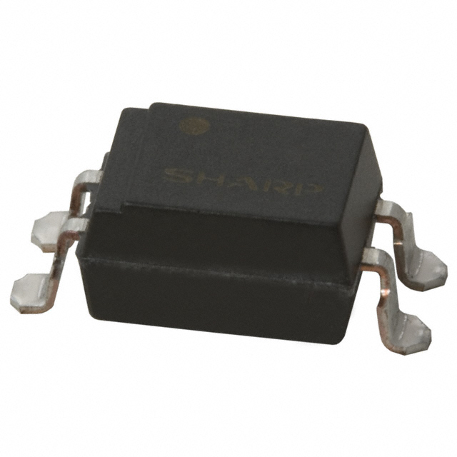
Product Overview: Sharp PC3H7B Optoisolator
The Sharp PC3H7B optoisolator leverages phototransistor coupling to enable robust signal isolation between input and output circuits. At its core, the device integrates an infrared-emitting diode and a phototransistor within a single encapsulated module. Electrical input, applied to the LED, transforms into an optical signal—instantly traversing the isolation barrier—then, the phototransistor detects and converts this back into an electrical output. This arrangement capitalizes on the lack of physical conductivity between input and output, effectively suppressing electrical noise propagation, and mitigating risk of destructive transients entering low-voltage domains.
Its reinforced isolation voltage of 2500 Vrms stems from precise internal clearances and optimized encapsulation materials, which guarantee resilience against high-potential surges. Such parameters prove essential for application in switching power supplies, inverter control circuitry, and communication interfaces, where differential ground potentials or periodic spikes threaten component integrity. In practical integration, the PC3H7B’s compact 4-Mini-Flat package facilitates high-density PCB layouts—critical for modern system designs requiring space-efficient, scalable isolation solutions.
The single-channel configuration is well-suited for scenarios demanding targeted isolation, such as microcontroller GPIO protection, where selective decoupling of signal lines reduces vulnerability without introducing unnecessary complexity. Deployment of the PC3H7B within digital feedback loops, relay drivers, and PLC I/O modules consistently enhances noise immunity and system robustness. Through direct experience, pairing the PC3H7B with careful layout practices—such as minimizing stray capacitance on isolated nodes and implementing guard traces—optimizes transient response and preserves isolation reliability under rapidly changing load conditions.
A noteworthy engineering insight emerges from considering the physical properties of the optoisolator package in thermal management: its reduced footprint assists in mitigating thermal gradients across the PCB, contributing to long-term package stability and consistent optoelectronic performance. The device’s response time and output characteristics should be carefully matched to the timing requirements of the target interface, especially in systems where propagation delay could impact real-time control fidelity.
By integrating the PC3H7B optoisolator into power electronics and automation systems, designers achieve not only basic signal isolation but also an additional layer of operational security against unpredictable electrical influences. This dual role—component-level protection and system-wide reliability—positions the PC3H7B as a fundamental building block in both legacy and state-of-the-art circuit architectures.
Key Features of the Sharp PC3H7B Optoisolator
The Sharp PC3H7B optoisolator is engineered to address stringent electrical isolation and control challenges in compact, high-density designs. At the core of its technical foundation lies the 2500 Vrms isolation voltage, achieved through precision-manufactured internal spacing and optimized optical coupling. This threshold not only ensures robust surge tolerance but also effectively suppresses ground loop interference and transient propagation. Isolation at this magnitude enables reliable interfacing between circuits operating at markedly different voltage domains, which is crucial for both device longevity and regulatory compliance in industrial, medical, and instrumentation environments.
The device employs a phototransistor-based output stage, capitalizing on the linearity and speed characteristics inherent to this architecture. The direct compatibility with a wide range of voltage levels—common to both analog and digital domains—simplifies driver circuitry design and fault monitoring strategies. This output modality enables deterministic signal transfer with minimal propagation delay. For developers, such architecture supports both clean switching of logic signals and proportional analog transmission, providing a flexible basis for mixed-signal circuit protection as well as data acquisition systems.
Physical design further advances the optoisolator’s integration value. The 4-Mini-Flat package reduces the component footprint, an essential feature in the ongoing trend toward higher PCB densities and multi-function modules. More aggressive component placement is possible without compromising isolation distances, streamlining both manual and automated assembly processes. In practice, this dimensioning minimizes board area overhead in converters, power controllers, and sensor nodes, where a balance of reliability and size is indispensable.
The single-channel configuration selectively targets node-to-node isolation scenarios. Unlike multi-channel alternatives, the mono-channel approach eliminates internal crosstalk and simplifies wiring complexity. This is highly advantageous in real-time control circuits, small-scale data links, and isolated feedback paths found within switching regulators or relay interfaces. Reduced parasitic interactions lead to lower noise injection and greater accuracy in feedback-critical applications.
Through these combined features, the PC3H7B illustrates a design philosophy grounded in precise engineering trade-offs—optimizing for isolation performance, application versatility, and PCB real estate. In iterative design cycles, the component has demonstrated stability under repetitive surge events and thermal cycling, as well as functional integrity during signal transitions close to its rated limits. Adaptability to rapidly evolving control logic standards further amplifies its relevance within the broader context of automation and connected device deployments. The single-channel, compact, phototransistor-outlined isolation offered by the PC3H7B thus serves as a pragmatic solution for designers prioritizing predictable behavior, electrical safety, and integration efficiency.
Typical Applications for the Sharp PC3H7B Optoisolator
The PC3H7B optoisolator demonstrates distinctive utility in electrical systems where signal integrity and galvanic isolation are paramount. Its operational core relies on optically-coupled input-output decoupling, driven by an integrated infrared LED and a phototransistor arranged in a compact package. This optical barrier forms the basis for robust isolation performance, typically exceeding 5000 Vrms. As a result, interface circuits can be designed to traverse domains with disparate voltage potentials or noise profiles without risk of unwanted conduction or logic contamination.
In feedback loops within switching-mode power supplies, the PC3H7B refines loop stability. Isolation cancels common-mode spikes and ground loop errors that proliferate across transformer primary windings. Its low saturation voltage and fast response facilitate precise feedback of error signals, maintaining tight regulation even under dynamic load changes. Close attention to transistor drive characteristics and minimal collector-emitter leakage ensures the feedback signal’s fidelity. Practical circuit layouts often embed the optoisolator as the only connection between secondary and primary sides, with careful PCB partitioning to further maximize noise immunity.
Microcontroller-based circuit nodes exploiting the PC3H7B gain a protective buffer against high-energy transients or erratic external switching. The optoisolator’s input threshold aligns well with typical logic voltage rails, enabling seamless integration with GPIOs. Use in input protection schemes circumvents the need for complex clamping networks by harnessing the inherent isolation—biasing recommendations ensure current-limiting resistors are sized for both LED longevity and digital edge speed. Development experience reveals that optoisolator-based interfaces sustain greater uptime when exposed to unpredictable field wiring or relay-induced surges.
In industrial automation, the PC3H7B delivers resilience against electromagnetic interference, ground potential shifts, and high-frequency noise. Integration within PLC I/O rungs or distributed sensor hubs is enhanced by the optoisolator’s form factor, which suits modular DIN rail mounting and high-density terminal blocks. Deployment patterns show that the optoisolator enables system expansion without compromising baseline insulation standards. Pairing with TVS diodes and robust filtering on the input side typically increases endurance in electrically noisy plant environments.
Medical and consumer device architectures increasingly leverage the PC3H7B to maintain clear division between patient-accessible controls and remote actuators or power sections. Its certified isolation distance aids compliance with electrical safety regimes such as IEC 60601. The optoisolator’s minimal propagation delay maintains responsive user interfaces even when driving relays or solenoids over isolated links. Real-world equipment designs incorporate redundant optoisolator pairs for critical signal paths, providing fault tolerance and ensuring circuit integrity through failure modes.
Strategic adoption of the PC3H7B enables system architectures to meet hard regulatory boundaries and operational dependability requirements. Its application highlights the importance of selecting isolation devices not merely by voltage rating, but also by switching performance, mechanical fit, and lifecycle reliability. This approach allows for the formulation of compact, safe, and highly responsive interface circuits positioned at the intersection of power conversion, logic control, and human interaction domains.
Package Details and Mechanical Considerations: Sharp PC3H7B Optoisolator
The adoption of the Sharp PC3H7B in its 4-Mini-Flat package configuration introduces significant mechanical and operational advantages, directly supporting high-density electronic design and robust system architecture. At a foundational level, the Mini-Flat form factor addresses core requirements for space efficiency and manufacturability. Its low-profile geometry reduces the mounting area compared to conventional dual in-line packages (DIPs), enabling increased component density on multilayer PCBs. This compactness translates into shorter signal traces, lowering potential for parasitic coupling and thereby improving signal integrity—a subtle but crucial advantage in high-frequency and precision interface circuits.
Mechanical stability is further enhanced by the encapsulated construction, which shields the internal optoelectronic interface from particulate ingress and environmental contaminants. The resin package not only moderates internal stresses during thermal cycling but also minimizes refractive index variations along the optical path. These attributes elevate the optoisolator’s reliability profile, delivering predictable isolation performance even in harsh industrial or automotive control environments. In practical deployment, such reliability mitigates maintenance interventions and ensures longer service intervals for fielded assemblies.
From a manufacturing perspective, the 4-Mini-Flat outlines are engineered for seamless integration with automated assembly workflows. The carefully defined lead spacing and coplanarity conform to standard pick-and-place tolerances, facilitating rapid processing on high-throughput SMT lines with minimal risk of misalignment or solder defects. Consistent package dimensions also simplify profile development for reflow soldering, supporting both traditional tin-lead and modern lead-free processes. Lessons from volume production highlight that the Mini-Flat package's robust leads minimize instances of PCB pad lift or thermal/mechanical stress-induced failures, sustaining yield rates even under aggressive throughput targets.
Application scenarios see substantial benefits from these characteristics. Dense power management PCBs and safety-critical modules—where spatial constraints are severe and error tolerance is minimal—leverage the optoisolator’s streamlined footprint. The combination of mechanical resilience and assembly flexibility positions the device for reliable galvanic isolation in feedback, gate drive, and digital communication links. Observations from long-term deployment indicate reduced failure rates associated with solder joint fatigue and optical path degradation, affirming the package’s suitability for mission-critical infrastructure.
A distinguishing insight is that the 4-Mini-Flat package, beyond addressing immediate board-level design priorities, subtly transforms system-level reliability strategy. Its mechanical and assembly advantages enable a more aggressive component placement philosophy, supporting the evolution of compact, feature-rich embedded systems without conceding maintainability or lifecycle stability. This synergy between mechanical engineering and functional performance establishes a basis for scalable, high-reliability optoisolation in next-generation electronics design.
Potential Equivalent/Replacement Models for Sharp PC3H7B Optoisolator
Evaluating potential substitutes for the Sharp PC3H7B demands a methodical approach centered on electrical, mechanical, and regulatory alignment. The primary function of the PC3H7B—a phototransistor output optoisolator in a Mini-Flat package—relies on robust input-to-output isolation, making its 2500 Vrms isolation voltage specification a non-negotiable baseline for any equivalent device. Maintaining this isolation barrier is essential for system safety in environments subject to high-voltage transients or strict regulatory standards.
Beyond isolation, the package footprint and pin configuration influence the ease of drop-in replacement. Mini-Flat packages offer space efficiency for high-density PCBs. Ensuring dimensional compatibility minimizes board redesign and maintains manufacturability, especially in automated SMT assembly processes. Attention to interface polarity, CTR (Current Transfer Ratio), and V_CE(sat) figures is also critical. Variances here can undermine signal integrity or introduce timing mismatches, particularly in analog or gating applications where subtle changes propagate system-level effects.
Typical alternative models for the PC3H7B include optoisolators from broadline suppliers—such as Toshiba’s TLP785 or Lite-On’s LTV-817 series—which replicate the isolation voltage, offer phototransistor outputs, and conform to similar package outlines. Devices adhering to industrial safety standards like UL or VDE gain priority in qualified designs, as transferring approvals from one certified model to another streamlines compliance. In fast-moving production environments, established dual-sourcing strategies leverage such compatible families to mitigate component shortages or end-of-life disruptions, securing supply chains without expensive requalification efforts.
When integrating substitute devices, empirical verification remains pivotal. Subtle differences in CTR distribution or response times may only present under real load conditions. Practical experience shows that performing side-by-side dynamic tests of signal fidelity, temperature stability, and long-term aging provides early detection of marginal incompatibilities that data sheets may not flag. Pursuing this layered validation approach uncovers nuanced system interactions, supporting robust lifecycle management.
Ultimately, the optimal replacement model balances strict electrical parity with accessible procurement and proven reliability. Sourcing from second-tier or lesser-known vendors merits added scrutiny of support documentation, lot-to-lot consistency, and long-term availability. Integrating replacement optoisolators in high-reliability applications benefits from maintaining vendor diversity, enabling agile response to market uncertainties while prioritizing electrical performance and regulatory continuity above superficial equivalence.
Conclusion
The Sharp PC3H7B Optoisolator demonstrates robust performance in high-demand signal isolation, leveraging its reinforced insulation of 2500 Vrms. This elevated isolation threshold is achieved through optimized internal die spacing and advanced molding techniques, mitigating risks of dielectric breakdown even in transient-heavy industrial contexts. The device features a phototransistor output architecture, establishing a linear response window suitable for TTL and logic-level interfacing, without imposing additional complexity on signal conditioning circuits.
The package design, a 4-Mini-Flat format, directly addresses real estate constraints in densely populated PCBs. Its slim profile and standardized pinout enable confident routing in multi-layer board layouts while reducing parasitic capacitance that might otherwise degrade high-frequency response or introduce unwanted cross-talk. Reliability is further strengthened by the selection of stable optical coupler materials, which exhibit minimal sensitivity to ambient temperature excursions, ensuring consistent isolation over extended operational lifespans in tightly regulated medical, instrumentation, or industrial control assemblies.
In practical deployment, the PC3H7B’s electrical and mechanical attributes simplify certification navigation, particularly for systems governed by international safety standards such as IEC 60950 or UL 1577. Integrating the component into isolation barriers adjacent to fault-prone field interfaces, such as relay drivers or sensor loops, has proven to effectively partition critical subsystems, supporting fail-safe strategies in mission-critical electronics. Comparative evaluation with alternatives often highlights the superior noise rejection and reduced placement constraints of this optoisolator, especially when designing for automated assembly or miniaturized product enclosures.
A nuanced perspective reveals that specifying the PC3H7B extends beyond mere compliance; the approach aligns isolation strength, physical footprint, and interface compatibility, targeting the convergence point where system safety, integration efficiency, and cost containment meet. When applied in closed-loop power supplies, digital control planes, or galvanically isolated communication links, the device’s construction facilitates enduring signal fidelity while streamlining board-level engineering. This layered optimization supports design teams in achieving higher system availability and broader regulatory acceptance, proving the practical advantages rooted in both component selection and deployment methodology.