


Request Quote
(Ships tomorrow)
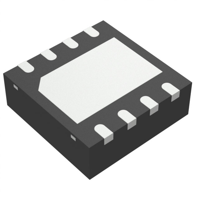
ZXMC3AM832TA MOSFET N/P-Channel Equivalent & Substitute Parts
Part Overview
The ZXMC3AM832TA is a dual MOSFET array integrating N-channel and P-channel transistors in a compact 8-MLP surface mount package. Manufactured by Diodes Incorporated, this device is rated for 30V drain-to-source voltage with continuous drain currents of 2.9A (N-channel) and 2.1A (P-channel). The component features logic level gate operation and is designed for general-purpose switching and amplification applications.
The ZXMC3AM832TA carries an obsolete product status. Locating equivalent or substitute components becomes necessary for ongoing production support, design updates, or inventory replenishment when original stock becomes unavailable. Active alternatives with identical or compatible electrical specifications are available from the same manufacturer.
Substiute Parts
Key Parameters
| Parameter | Value | Unit |
|---|---|---|
| Configuration | N and P-Channel | — |
| Drain to Source Voltage (Vdss) | 30 | V |
| Continuous Drain Current (Id) @ 25°C | 2.9A / 2.1A | A |
| On-State Resistance (Rds On Max) | 120 | mOhm @ 2.5A, 10V |
| Gate Threshold Voltage (Vgs(th) Max) | 1 | V @ 250µA (Min) |
| Gate Charge (Qg Max) | 3.9 | nC @ 10V |
| Input Capacitance (Ciss Max) | 190 | pF @ 25V |
| Maximum Power Dissipation | 1.7 | W |
| FET Feature | Logic Level Gate | — |
| Mounting Type | Surface Mount | — |
| Package Type | 8-VDFN Exposed Pad | — |
| RoHS Status | ROHS3 Compliant | — |
| Moisture Sensitivity Level | 1 (Unlimited) | — |
Substitute Part Grouping Explanation
Substitution of the ZXMC3AM832TA is determined by strict equivalence across the following critical electrical and mechanical parameters:
Electrical Equivalence Criteria:
- Dual N-channel and P-channel MOSFET configuration
- 30V drain-to-source voltage rating
- Continuous drain current ratings of 2.9A (N-channel) and 2.1A (P-channel)
- On-state resistance of 120 mOhm maximum at specified conditions
- Gate charge of 3.9 nC maximum at 10V
- Input capacitance of 190 pF maximum at 25V
- Logic level gate operation
- Maximum power dissipation of 1.7W
Mechanical Compatibility Criteria:
- Surface mount technology
- 8-pin package configuration
- Exposed pad thermal design
- Moisture sensitivity level MSL 1
Compliance Criteria:
- RoHS3 compliance
- REACH unaffected status
- EAR99 export classification
The ZXMC3AMCTA qualifies as a direct substitute based on identical electrical specifications and compatible package geometry, with the distinction of active product status and alternative packaging format.
Parameter Comparison
| Parameter | ZXMC3AM832TA (Main) | ZXMC3AMCTA (Substitute) | Match Status |
|---|---|---|---|
| Manufacturer | Diodes Incorporated | Diodes Incorporated | Identical |
| Configuration | N and P-Channel | N and P-Channel | Identical |
| Drain to Source Voltage (Vdss) | 30V | 30V | Identical |
| Continuous Drain Current (Id) @ 25°C | 2.9A / 2.1A | 2.9A / 2.1A | Identical |
| Rds On (Max) @ Id, Vgs | 120 mOhm @ 2.5A, 10V | 120 mOhm @ 2.5A, 10V | Identical |
| Gate Charge (Qg Max) @ Vgs | 3.9 nC @ 10V | 3.9 nC @ 10V | Identical |
| Input Capacitance (Ciss Max) @ Vds | 190 pF @ 25V | 190 pF @ 25V | Identical |
| Power - Max | 1.7W | 1.7W | Identical |
| FET Feature | Logic Level Gate | Logic Level Gate | Identical |
| Mounting Type | Surface Mount | Surface Mount | Identical |
| Package / Case | 8-VDFN Exposed Pad | 8-WDFN Exposed Pad | Compatible |
| Supplier Device Package | 8-MLP (3x2) | DFN3020B-8 | Compatible |
| Product Status | Obsolete | Active | Substitute is Active |
| RoHS Status | ROHS3 Compliant | ROHS3 Compliant | Identical |
| Moisture Sensitivity Level | 1 (Unlimited) | 1 (Unlimited) | Identical |
| REACH Status | REACH Unaffected | REACH Unaffected | Identical |
Engineering Selection Recommendations
ZXMC3AMCTA as Primary Substitute:
The ZXMC3AMCTA is the direct equivalent for the obsolete ZXMC3AM832TA. Both devices share identical electrical specifications across all critical parameters including voltage rating, current capacity, on-state resistance, gate charge, and input capacitance. The package designations (8-VDFN versus 8-WDFN) represent compatible DFN variants with equivalent thermal and electrical performance characteristics.
The ZXMC3AMCTA carries active product status, ensuring ongoing availability and manufacturing support. Both components maintain ROHS3 compliance and REACH unaffected status, satisfying current regulatory requirements. Moisture sensitivity level MSL 1 is identical for both parts, indicating unlimited shelf life under standard storage conditions.
The substitute part is supplied in Tape & Reel packaging format, standard for production environments. The operating temperature range of -55°C to 150°C (junction temperature) for the ZXMC3AMCTA provides the thermal operating window for this device class.
Selection Basis:
Component selection between the main part and substitute is determined by product availability and supply chain requirements. The ZXMC3AMCTA is the recommended choice for new designs and ongoing production due to its active status and guaranteed long-term availability.
Frequently Asked Questions (FAQ)
Q: Can the ZXMC3AMCTA directly replace the ZXMC3AM832TA in existing designs?
A: Yes. The ZXMC3AMCTA provides direct electrical equivalence across all specified parameters. Both devices feature identical voltage ratings, current ratings, on-state resistance, gate charge, and input capacitance. The package variants (8-VDFN and 8-WDFN) are compatible DFN configurations with equivalent pin assignments and thermal characteristics.
Q: What is the difference between the 8-MLP and DFN3020B-8 package designations?
A: Both designations refer to 8-pin surface mount packages with exposed thermal pads in a 3x2mm footprint. The 8-MLP (Micro Lead Package) and DFN3020B-8 (Dual Flat No-Lead) are compatible package variants from Diodes Incorporated. PCB layout and thermal management considerations remain equivalent between the two package types.
Q: Why is the ZXMC3AM832TA marked as obsolete?
A: Product obsolescence reflects manufacturing lifecycle decisions by Diodes Incorporated. The ZXMC3AMCTA represents the active continuation of this device family with identical electrical performance and improved supply chain availability.
Q: Are there any compliance differences between the two parts?
A: No. Both the ZXMC3AM832TA and ZXMC3AMCTA maintain ROHS3 compliance, REACH unaffected status, and MSL 1 moisture sensitivity rating. Regulatory and environmental compliance requirements are satisfied identically by both components.
Q: What is the significance of the logic level gate feature?
A: Logic level gate operation indicates that the MOSFET can be fully switched using standard digital logic voltage levels (typically 3.3V or 5V). This feature enables direct interface with microcontroller outputs and digital signal processing circuits without requiring additional gate drive circuitry.
Q: How does the gate charge specification affect circuit design?
A: Gate charge (Qg) of 3.9 nC determines the switching speed and gate drive current requirements. Lower gate charge enables faster switching transitions and reduces power dissipation in the gate drive circuit. This specification is identical between the main part and substitute, ensuring equivalent switching performance.
Q: Is the exposed pad thermal design critical for this application?
A: The exposed pad provides direct thermal coupling to the PCB, enabling efficient heat dissipation from the 1.7W maximum power rating. Both package variants include exposed pads with equivalent thermal performance. Proper PCB layout with adequate copper area connected to the exposed pad is required for optimal thermal management.
Alternative Parts

SJ6012L2TP
Littelfuse Inc.
6 Alternative Parts

JMK107BBJ476MA-RE
Taiyo Yuden
10 Alternative Parts

GMK107BBJ475MA-T
Taiyo Yuden
5 Alternative Parts
SJ6020N2ARP
Littelfuse Inc.
3 Alternative Parts
SJ6025R2ATP
Littelfuse Inc.
4 Alternative Parts

2474-05L
API Delevan Inc.
1 Alternative Parts

4590R-684K
API Delevan Inc.
1 Alternative Parts

CM6560R-334
API Delevan Inc.
1 Alternative Parts

CM6460-104
API Delevan Inc.
1 Alternative Parts

5526-12
API Delevan Inc.
1 Alternative Parts