


Request Quote
(Ships tomorrow)
ZVP0545ASTZ P-Channel MOSFET Equivalent & Substitute Parts
Part Overview
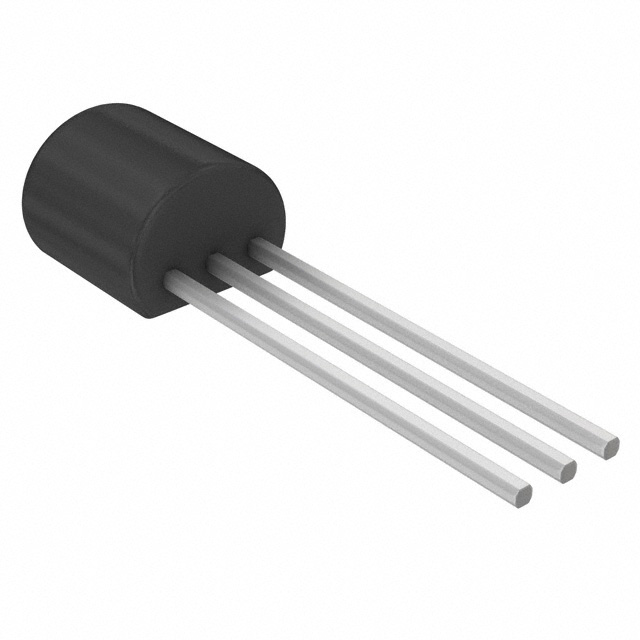
The ZVP0545ASTZ is an active P-Channel MOSFET manufactured by Diodes Incorporated, rated for 450V drain-to-source voltage with 45mA continuous drain current. This device is packaged in an E-Line (TO-92 compatible) through-hole configuration and is designed for applications requiring high-voltage P-channel switching or amplification. The part is RoHS3 compliant and carries unlimited moisture sensitivity classification.
Substitute parts are identified when equivalent electrical performance can be maintained within the specified parameter ranges while accommodating standard package variations in the through-hole MOSFET category.
Substiute Parts
Key Parameters
| Parameter | Value | Unit |
|---|---|---|
| FET Type | P-Channel | — |
| Drain-to-Source Voltage (Vdss) | 450 | V |
| Continuous Drain Current (Id) @ 25°C | 45 | mA |
| Gate-Source Threshold Voltage (Vgs(th)) @ 1mA | 4.5 | V |
| Gate-Source Voltage (Vgs Max) | ±20 | V |
| On-State Drain Resistance (Rds On) @ 50mA, 10V | 150 | Ohm |
| Input Capacitance (Ciss) @ 25V | 120 | pF |
| Power Dissipation (Max) | 700 | mW |
| Operating Temperature Range | -55 to 150 | °C |
| Mounting Type | Through Hole | — |
| Package Type | E-Line-3 (TO-92 compatible) | — |
| RoHS Status | ROHS3 Compliant | — |
Substitute Part Grouping Explanation
Substitution of the ZVP0545ASTZ is determined by the following critical electrical and mechanical parameters:
Electrical Compatibility Criteria:
- FET Type: P-Channel topology must be maintained
- Drain-to-Source Voltage (Vdss): Substitute must equal or exceed 450V
- Continuous Drain Current (Id): Substitute must equal or exceed 45mA at rated temperature
- Gate-Source Threshold Voltage (Vgs(th)): Must remain within ±20V gate-source voltage specification
- On-State Resistance (Rds On): Lower or equivalent values are acceptable
- Operating Temperature Range: Must support -55°C to 150°C operation
- Power Dissipation: Equal or higher ratings are acceptable
Mechanical Compatibility Criteria:
- Mounting Type: Through-hole configuration required
- Package Compatibility: TO-92 family packages (E-Line-3, TO-92-3, TO-226-3) are mechanically compatible
- Pin Configuration: Three-terminal through-hole devices with identical pinout function
The VP0550N3-G from Microchip Technology meets all substitution criteria with improved electrical performance in key parameters.
Parameter Comparison
| Parameter | ZVP0545ASTZ (Diodes Inc.) | VP0550N3-G (Microchip) | Unit |
|---|---|---|---|
| FET Type | P-Channel | P-Channel | — |
| Drain-to-Source Voltage (Vdss) | 450 | 500 | V |
| Continuous Drain Current (Id) @ 25°C | 45 | 54 | mA |
| Gate-Source Threshold Voltage (Vgs(th)) @ 1mA | 4.5 | 4.5 | V |
| Gate-Source Voltage (Vgs Max) | ±20 | ±20 | V |
| On-State Drain Resistance (Rds On) @ 10V | 150 @ 50mA | 125 @ 10mA | Ohm |
| Input Capacitance (Ciss) @ 25V | 120 | 70 | pF |
| Power Dissipation (Max) | 700 | 1000 | mW |
| Operating Temperature Range | -55 to 150 | -55 to 150 | °C |
| Mounting Type | Through Hole | Through Hole | — |
| Package Type | E-Line-3 (TO-92 compatible) | TO-92-3 (TO-226-3) | — |
| RoHS Status | ROHS3 Compliant | ROHS3 Compliant | — |
Engineering Selection Recommendations
VP0550N3-G as Direct Substitute:
The VP0550N3-G from Microchip Technology is a qualified substitute for the ZVP0545ASTZ. Both devices are active products with ROHS3 compliance and REACH unaffected status, ensuring regulatory alignment.
The VP0550N3-G provides enhanced electrical performance across multiple parameters:
- Higher drain-to-source voltage rating (500V vs. 450V) provides increased voltage margin
- Higher continuous drain current (54mA vs. 45mA) accommodates higher current applications
- Lower on-state resistance (125Ohm vs. 150Ohm) reduces conduction losses
- Lower input capacitance (70pF vs. 120pF) improves switching speed
- Higher power dissipation rating (1W vs. 700mW) extends thermal headroom
Both devices maintain identical gate-source threshold voltage and maximum gate-source voltage specifications, ensuring gate drive circuit compatibility. Operating temperature ranges are identical, supporting the full -55°C to 150°C specification.
Package compatibility is confirmed through TO-92 family standardization. The TO-92-3 package of the VP0550N3-G is mechanically and functionally equivalent to the E-Line-3 package of the ZVP0545ASTZ in through-hole PCB applications.
Frequently Asked Questions (FAQ)
Q: Can the VP0550N3-G replace the ZVP0545ASTZ in existing designs without PCB modification?
A: Yes. Both devices use through-hole TO-92 family packages with identical three-terminal pinout configurations. No PCB layout changes are required for mechanical compatibility.
Q: What is the significance of the higher Vdss rating (500V vs. 450V) in the VP0550N3-G?
A: The higher drain-to-source voltage rating provides additional safety margin in applications operating near the 450V specification limit. This reduces the risk of device failure due to voltage transients or overshoot conditions.
Q: Are the gate drive requirements identical between these two devices?
A: Yes. Both devices have identical gate-source threshold voltage (4.5V @ 1mA) and maximum gate-source voltage (±20V) specifications. Existing gate drive circuits require no modification.
Q: How do the on-state resistance values compare, and what is the practical impact?
A: The VP0550N3-G has lower on-state resistance (125Ohm @ 10mA, 10V vs. 150Ohm @ 50mA, 10V). Lower on-state resistance reduces power dissipation during conduction, improving overall circuit efficiency and reducing thermal load.
Q: Are both devices compliant with current environmental and regulatory standards?
A: Yes. Both the ZVP0545ASTZ and VP0550N3-G are ROHS3 compliant and REACH unaffected, meeting current environmental regulations for electronic components.
Q: What is the difference in input capacitance, and does it affect circuit design?
A: The VP0550N3-G has lower input capacitance (70pF vs. 120pF @ 25V). Lower input capacitance reduces gate charge requirements and improves switching speed, which can reduce switching losses in high-frequency applications.
Q: Can these devices be used interchangeably in high-temperature applications?
A: Yes. Both devices support the full -55°C to 150°C operating temperature range. Thermal performance depends on application-specific power dissipation and thermal management design.
Alternative Parts

SJ6012L2TP
Littelfuse Inc.
6 Alternative Parts

JMK107BBJ476MA-RE
Taiyo Yuden
10 Alternative Parts

GMK107BBJ475MA-T
Taiyo Yuden
5 Alternative Parts
SJ6020N2ARP
Littelfuse Inc.
3 Alternative Parts
SJ6025R2ATP
Littelfuse Inc.
4 Alternative Parts

2474-05L
API Delevan Inc.
1 Alternative Parts

4590R-684K
API Delevan Inc.
1 Alternative Parts

CM6560R-334
API Delevan Inc.
1 Alternative Parts

CM6460-104
API Delevan Inc.
1 Alternative Parts

5526-12
API Delevan Inc.
1 Alternative Parts