


Request Quote
(Ships tomorrow)
VS3674UNION Equivalent & Substitute Parts
Part Overview
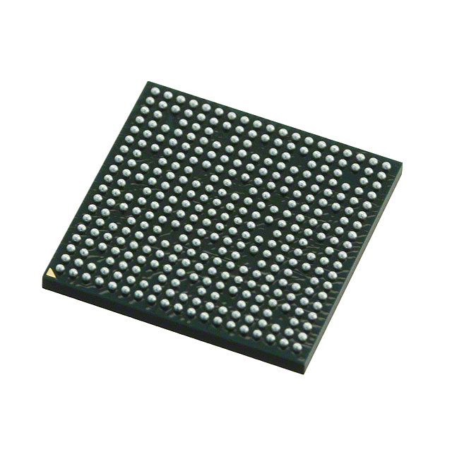
The VS3674UNION is a Digital Media System-on-Chip (DMSoC) from Texas Instruments' TMS320DM3x DaVinci™ series, designed for embedded multimedia processing applications. This device integrates a 432MHz processor with comprehensive multimedia interfaces including Ethernet, USB, SPI, I2C, and McBSP connectivity. The part is currently in Last Time Buy status, indicating end-of-life transition. Identifying qualified substitute components is essential for design continuity and long-term product support.
Substiute Parts
Key Parameters
| Parameter | VS3674UNION |
|---|---|
| Manufacturer | Texas Instruments |
| Series | TMS320DM3x, DaVinci™ |
| Package / Case | 338-LFBGA (13x13) |
| Clock Rate | 432MHz |
| On-Chip RAM | 56kB |
| Non-Volatile Memory | ROM (16kB) |
| Voltage - Core | 1.35V |
| Voltage - I/O | 1.8V, 3.3V |
| Operating Temperature | 0°C ~ 85°C (TC) |
| Interface | EBI/EMI, Ethernet, I2C, McBSP, SPI, UART, USB |
| RoHS Status | ROHS3 Compliant |
| MSL Rating | 3 (168 Hours) |
Substitute Part Grouping Explanation
Substitution eligibility for the VS3674UNION is determined by the following critical parameters:
Package Compatibility: The 338-LFBGA (13x13) package footprint must be identical to ensure PCB layout compatibility without redesign.
Interface Compatibility: All required interfaces (EBI/EMI, Ethernet, I2C, McBSP, SPI, UART, USB) must be present to maintain functional equivalence.
Memory Configuration: On-chip RAM (56kB) and ROM (16kB) specifications must match to preserve software compatibility and memory allocation schemes.
Voltage Specifications: Core voltage (1.35V) and I/O voltage levels (1.8V, 3.3V) must be supported to ensure proper operation with existing power delivery and signal conditioning circuits.
Temperature Range: Operating temperature range 0°C ~ 85°C (TC) must be maintained for thermal design compatibility.
Compliance Standards: RoHS3 compliance and MSL rating 3 (168 Hours) must be preserved for manufacturing and reliability requirements.
The TMS320DM365ZCE21 meets these substitution criteria within the TMS320DM3x DaVinci™ product family.
Parameter Comparison
| Parameter | VS3674UNION | TMS320DM365ZCE21 | Compatibility |
|---|---|---|---|
| Manufacturer | Texas Instruments | Texas Instruments | Match |
| Series | TMS320DM3x, DaVinci™ | TMS320DM3x, DaVinci™ | Match |
| Package / Case | 338-LFBGA (13x13) | 338-LFBGA (13x13) | Match |
| Clock Rate | 432MHz | 216MHz | Difference |
| On-Chip RAM | 56kB | 56kB | Match |
| Non-Volatile Memory | ROM (16kB) | ROM (16kB) | Match |
| Voltage - Core | 1.35V | 1.20V | Difference |
| Voltage - I/O | 1.8V, 3.3V | 1.8V, 3.3V | Match |
| Operating Temperature | 0°C ~ 85°C (TC) | 0°C ~ 85°C (TC) | Match |
| Interface | EBI/EMI, Ethernet, I2C, McBSP, SPI, UART, USB | EBI/EMI, Ethernet, I2C, McBSP, SPI, UART, USB | Match |
| RoHS Status | ROHS3 Compliant | ROHS3 Compliant | Match |
| MSL Rating | 3 (168 Hours) | 3 (168 Hours) | Match |
| Product Status | Last Time Buy | Active | Substitute is Active |
Engineering Selection Recommendations
The TMS320DM365ZCE21 is the qualified substitute for the VS3674UNION based on the following engineering criteria:
Package and Pinout: Both devices utilize the 338-LFBGA (13x13) package, enabling direct PCB layout compatibility without redesign.
Interface Equivalence: The substitute maintains all required interfaces (EBI/EMI, Ethernet, I2C, McBSP, SPI, UART, USB), ensuring functional compatibility with existing system architecture.
Memory Compatibility: Identical on-chip RAM (56kB) and ROM (16kB) configurations preserve software compatibility and memory allocation schemes.
Voltage Support: Both devices support 1.8V and 3.3V I/O voltages. The substitute's 1.20V core voltage differs from the original 1.35V; power delivery circuits must be evaluated for compatibility with this specification.
Compliance and Reliability: The substitute maintains ROHS3 compliance and MSL rating 3 (168 Hours), meeting manufacturing and environmental requirements.
Product Status: The substitute is in Active status, providing long-term availability and supply chain stability compared to the Last Time Buy status of the original part.
Performance Consideration: The substitute operates at 216MHz clock rate versus the original 432MHz. Applications requiring the original performance specification must evaluate whether this reduction impacts system requirements.
Frequently Asked Questions (FAQ)
Q: Can the TMS320DM365ZCE21 be used as a direct replacement for the VS3674UNION without PCB modifications?
A: Yes, the identical 338-LFBGA (13x13) package footprint and pinout enable direct PCB compatibility. However, power delivery circuits must be evaluated for the 1.20V core voltage specification of the substitute.
Q: What is the primary difference between these two devices?
A: The clock rate differs: VS3674UNION operates at 432MHz while TMS320DM365ZCE21 operates at 216MHz. The substitute also requires 1.20V core voltage versus 1.35V for the original. All other specifications including interfaces, memory, and package are equivalent.
Q: Are the interface specifications identical between the two parts?
A: Yes, both devices provide identical interface support: EBI/EMI, Ethernet, I2C, McBSP, SPI, UART, and USB. No interface modifications are required for substitution.
Q: Does the substitute maintain the same memory configuration?
A: Yes, both devices feature 56kB on-chip RAM and 16kB ROM, ensuring software compatibility and identical memory allocation schemes.
Q: What is the significance of the product status difference?
A: The VS3674UNION is in Last Time Buy status, indicating end-of-life transition with limited future availability. The TMS320DM365ZCE21 is in Active status, providing long-term supply chain stability and continued manufacturer support.
Q: Are there any compliance or environmental differences?
A: No, both devices are ROHS3 compliant with MSL rating 3 (168 Hours), meeting identical manufacturing and environmental requirements.
Q: How should the clock rate difference be evaluated for my application?
A: The 216MHz clock rate of the substitute is half that of the original 432MHz device. Applications must assess whether this performance reduction impacts system throughput, processing latency, or real-time requirements. Thermal and power consumption characteristics may also differ.
Alternative Parts

SJ6012L2TP
Littelfuse Inc.
6 Alternative Parts

JMK107BBJ476MA-RE
Taiyo Yuden
10 Alternative Parts

GMK107BBJ475MA-T
Taiyo Yuden
5 Alternative Parts
SJ6020N2ARP
Littelfuse Inc.
3 Alternative Parts
SJ6025R2ATP
Littelfuse Inc.
4 Alternative Parts

2474-05L
API Delevan Inc.
1 Alternative Parts

4590R-684K
API Delevan Inc.
1 Alternative Parts

CM6560R-334
API Delevan Inc.
1 Alternative Parts

CM6460-104
API Delevan Inc.
1 Alternative Parts

5526-12
API Delevan Inc.
1 Alternative Parts