


Request Quote
(Ships tomorrow)
VCBU68WMCE30 Equivalent & Substitute Parts
Part Overview
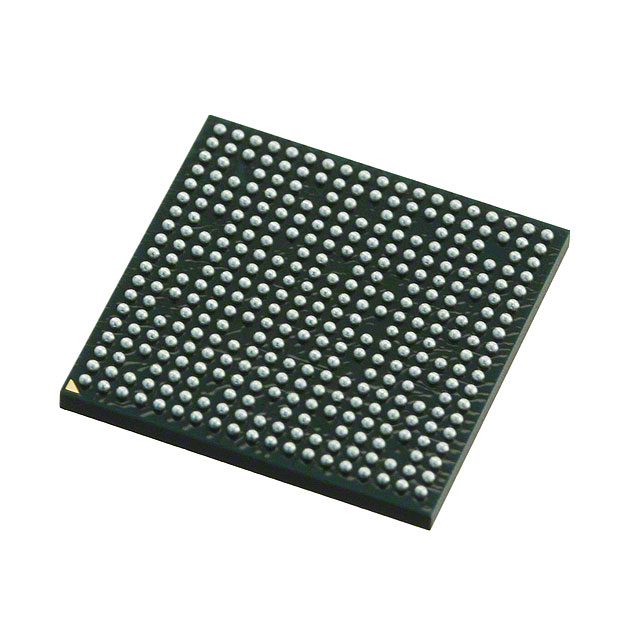
The VCBU68WMCE30 is a Digital Media System-on-Chip (DMSoC) from Texas Instruments' TMS320DM3x DaVinci™ series, designed for embedded multimedia processing applications. This device integrates a 432MHz processor with comprehensive multimedia interfaces including Ethernet, USB, SPI, I2C, and McBSP connectivity. The part carries Last Time Buy status, indicating end-of-life production. Identifying equivalent substitute components is essential for design continuity and long-term product support.
Substiute Parts
Key Parameters
| Parameter | Value |
|---|---|
| Manufacturer Part Number | VCBU68WMCE30 |
| Manufacturer | Texas Instruments |
| Series | TMS320DM3x, DaVinci™ |
| Package / Case | 338-LFBGA (13x13) |
| Clock Rate | 432MHz |
| On-Chip RAM | 56kB |
| Non-Volatile Memory | ROM (16kB) |
| Voltage - Core | 1.35V |
| Voltage - I/O | 1.8V, 3.3V |
| Operating Temperature | 0°C ~ 85°C (TC) |
| Interface | EBI/EMI, Ethernet, I2C, McBSP, SPI, UART, USB |
| Product Status | Last Time Buy |
| RoHS Status | ROHS3 Compliant |
| MSL Rating | 3 (168 Hours) |
Substitute Part Grouping Explanation
Substitution eligibility for the VCBU68WMCE30 is determined by the following critical parameters:
- Package compatibility: 338-LFBGA (13x13) form factor
- Interface set: EBI/EMI, Ethernet, I2C, McBSP, SPI, UART, USB
- Memory configuration: 56kB on-chip RAM and 16kB ROM
- Voltage rails: 1.8V/3.3V I/O and core voltage support
- Operating temperature range: 0°C ~ 85°C
- Series family: TMS320DM3x DaVinci™
The TMS320DM365ZCE21 qualifies as a substitute based on identical package, interface set, memory configuration, voltage specifications, and temperature range. Differences in clock rate (216MHz vs. 432MHz) and core voltage (1.20V vs. 1.35V) represent functional variations within the same product family and do not preclude substitution where performance requirements permit.
Parameter Comparison
| Parameter | VCBU68WMCE30 | TMS320DM365ZCE21 |
|---|---|---|
| Manufacturer | Texas Instruments | Texas Instruments |
| Series | TMS320DM3x, DaVinci™ | TMS320DM3x, DaVinci™ |
| Package / Case | 338-LFBGA (13x13) | 338-LFBGA (13x13) |
| Clock Rate | 432MHz | 216MHz |
| On-Chip RAM | 56kB | 56kB |
| Non-Volatile Memory | ROM (16kB) | ROM (16kB) |
| Voltage - Core | 1.35V | 1.20V |
| Voltage - I/O | 1.8V, 3.3V | 1.8V, 3.3V |
| Operating Temperature | 0°C ~ 85°C (TC) | 0°C ~ 85°C (TC) |
| Interface | EBI/EMI, Ethernet, I2C, McBSP, SPI, UART, USB | EBI/EMI, Ethernet, I2C, McBSP, SPI, UART, USB |
| Mounting Type | Surface Mount | Surface Mount |
| RoHS Status | ROHS3 Compliant | ROHS3 Compliant |
| MSL Rating | 3 (168 Hours) | 3 (168 Hours) |
| Product Status | Last Time Buy | Active |
Engineering Selection Recommendations
The TMS320DM365ZCE21 is the designated substitute for the VCBU68WMCE30. Both devices maintain identical mechanical and electrical compatibility through matching package specifications, interface configurations, and voltage requirements. The substitute part carries Active product status, ensuring continued availability and manufacturing support, whereas the original part is in Last Time Buy phase.
Selection of the TMS320DM365ZCE21 is appropriate for applications where the reduced clock rate (216MHz versus 432MHz) and lower core voltage (1.20V versus 1.35V) align with system performance requirements. Both parts maintain ROHS3 compliance and identical moisture sensitivity ratings, supporting equivalent supply chain and storage protocols.
Frequently Asked Questions (FAQ)
Q: Can the TMS320DM365ZCE21 be used as a direct replacement for the VCBU68WMCE30?
A: The TMS320DM365ZCE21 is mechanically and electrically compatible with the VCBU68WMCE30 in terms of package form factor, pinout, interface set, and voltage rails. Substitution is valid where application performance requirements accommodate the lower clock rate of 216MHz.
Q: What are the key differences between these parts?
A: The primary differences are clock rate (432MHz vs. 216MHz) and core voltage (1.35V vs. 1.20V). All other parameters—package, interfaces, memory, I/O voltage, and temperature range—are identical.
Q: Are there any compliance or certification differences?
A: Both parts maintain ROHS3 compliance, identical MSL ratings, and equivalent REACH and ECCN classifications. No compliance barriers exist to substitution.
Q: Does the lower clock rate affect PCB layout or thermal design?
A: The lower clock rate and reduced core voltage of the TMS320DM365ZCE21 typically result in lower power dissipation. Existing thermal and power delivery designs may require validation but generally support this substitution.
Q: What is the availability status of each part?
A: The VCBU68WMCE30 is in Last Time Buy status with limited inventory. The TMS320DM365ZCE21 maintains Active status with higher inventory availability, supporting long-term design continuity.
Alternative Parts

SJ6012L2TP
Littelfuse Inc.
6 Alternative Parts

JMK107BBJ476MA-RE
Taiyo Yuden
10 Alternative Parts

GMK107BBJ475MA-T
Taiyo Yuden
5 Alternative Parts
SJ6020N2ARP
Littelfuse Inc.
3 Alternative Parts
SJ6025R2ATP
Littelfuse Inc.
4 Alternative Parts

2474-05L
API Delevan Inc.
1 Alternative Parts

4590R-684K
API Delevan Inc.
1 Alternative Parts

CM6560R-334
API Delevan Inc.
1 Alternative Parts

CM6460-104
API Delevan Inc.
1 Alternative Parts

5526-12
API Delevan Inc.
1 Alternative Parts