


Request Quote
(Ships tomorrow)
TSV623AIST Equivalent & Substitute Parts
Part Overview
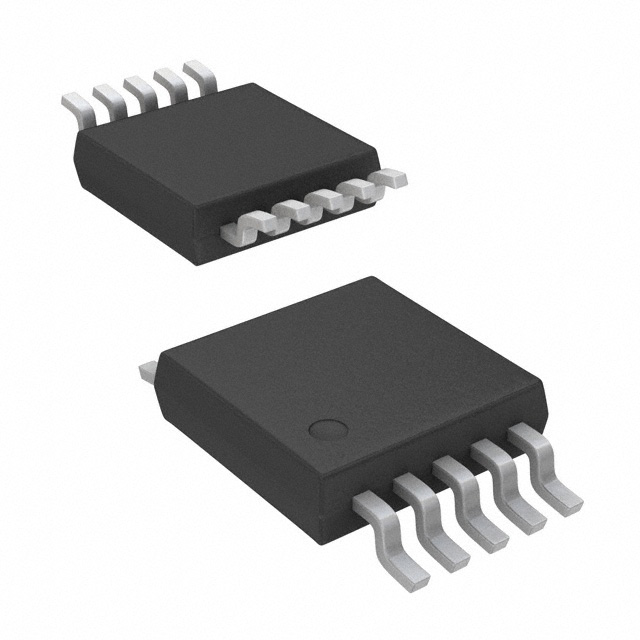
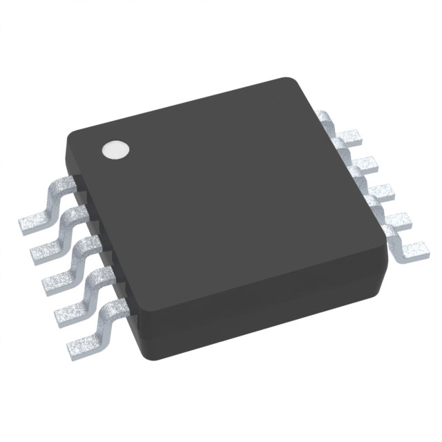
The TSV623AIST is an active linear amplifier integrated circuit manufactured by STMicroelectronics. This CMOS dual-channel operational amplifier features rail-to-rail output capability and is housed in a 10-MiniSO surface mount package. The device is classified as Active product status and is RoHS3 compliant. Substitute parts are identified when original inventory is unavailable, when alternative packaging formats are required, or when design specifications permit operation within the electrical and mechanical parameters of equivalent devices.
Substiute Parts
Key Parameters
| Parameter | Value | Unit |
|---|---|---|
| Manufacturer Part Number | TSV623AIST | — |
| Manufacturer | STMicroelectronics | — |
| Category | Linear, Amplifiers | — |
| Amplifier Type | CMOS | — |
| Number of Circuits | 2 | — |
| Output Type | Rail-to-Rail | — |
| Package / Case | 10-TFSOP, 10-MSOP (0.118", 3.00mm Width) | — |
| Mounting Type | Surface Mount | — |
| Voltage - Supply Span (Min) | 1.5 | V |
| Voltage - Supply Span (Max) | 5.5 | V |
| Operating Temperature | -40 to 125 | °C |
| Slew Rate | 0.14 | V/µs |
| Gain Bandwidth Product | 420 | kHz |
| Current - Input Bias | 1 | pA |
| Voltage - Input Offset | 1 | mV |
| Current - Supply | 29 | µA |
| Current - Output / Channel | 74 | mA |
| RoHS Status | ROHS3 Compliant | — |
| Product Status | Active | — |
Substitute Part Grouping Explanation
Substitute parts for the TSV623AIST are selected based on the following electrical and mechanical compatibility criteria:
Primary Substitution Criteria:
- Dual-channel (2 circuit) configuration
- Rail-to-rail output capability
- Surface mount package with 10-pin TFSOP/MSOP footprint (0.118", 3.00mm width)
- Operating temperature range overlap: -40°C to 125°C (or subset thereof)
- Supply voltage range compatibility: minimum 1.5V to 5.5V maximum (or subset thereof)
- RoHS3 compliance and REACH unaffected status
Secondary Compatibility Parameters:
- Slew rate, gain bandwidth product, input bias current, input offset voltage, supply current, and output current per channel are device-specific performance characteristics that determine functional equivalence within application-specific constraints.
The substitute parts identified below meet the primary mechanical and electrical compatibility criteria. Differences in secondary performance parameters reflect design variations between manufacturers and device series.
Parameter Comparison
| Parameter | TSV623AIST (STMicroelectronics) | LMV712Q1MM/NOPB (Texas Instruments) | LMV712Q1MMX/NOPB (Texas Instruments) | TLV2763IDGS (Texas Instruments) | TLV2763IDGSR (Texas Instruments) |
|---|---|---|---|---|---|
| Amplifier Type | CMOS | General Purpose | General Purpose | General Purpose | General Purpose |
| Number of Circuits | 2 | 2 | 2 | 2 | 2 |
| Output Type | Rail-to-Rail | Rail-to-Rail | Rail-to-Rail | Rail-to-Rail | Rail-to-Rail |
| Package / Case | 10-TFSOP, 10-MSOP | 10-TFSOP, 10-MSOP | 10-TFSOP, 10-MSOP | 10-TFSOP, 10-MSOP | 10-TFSOP, 10-MSOP |
| Mounting Type | Surface Mount | Surface Mount | Surface Mount | Surface Mount | Surface Mount |
| Voltage - Supply Span (Min) | 1.5 V | 2.7 V | 2.7 V | 1.8 V | 1.8 V |
| Voltage - Supply Span (Max) | 5.5 V | 5.5 V | 5.5 V | 3.6 V | 3.6 V |
| Operating Temperature | -40 to 125°C | -40 to 125°C | -40 to 125°C | -40 to 85°C | -40 to 85°C |
| Slew Rate | 0.14 V/µs | 5 V/µs | 5 V/µs | 0.23 V/µs | 0.23 V/µs |
| Gain Bandwidth Product | 420 kHz | 5 MHz | 5 MHz | 500 kHz | 500 kHz |
| Current - Input Bias | 1 pA | 5.5 pA | 5.5 pA | 3 pA | 3 pA |
| Voltage - Input Offset | 1 mV | 400 µV | 400 µV | 550 µV | 550 µV |
| Current - Supply | 29 µA | 1.22 mA (x2 Channels) | 1.22 mA (x2 Channels) | 20 µA (x2 Channels) | 20 µA (x2 Channels) |
| Current - Output / Channel | 74 mA | 50 mA | 50 mA | 10.2 mA | 10.2 mA |
| RoHS Status | ROHS3 Compliant | ROHS3 Compliant | ROHS3 Compliant | ROHS3 Compliant | ROHS3 Compliant |
| Product Status | Active | Active | Active | Active | Active |
Engineering Selection Recommendations
All identified substitute parts maintain Active product status and RoHS3 compliance, ensuring long-term availability and regulatory conformance equivalent to the TSV623AIST.
LMV712Q1MM/NOPB and LMV712Q1MMX/NOPB (Texas Instruments): These devices are qualified to AEC-Q100 automotive standards and support the full operating temperature range of -40°C to 125°C. Both parts are mechanically and electrically compatible with the TSV623AIST footprint. The LMV712Q1MMX/NOPB variant offers higher inventory availability (7300 units) compared to LMV712Q1MM/NOPB (1689 units). These devices exhibit higher slew rate (5 V/µs) and gain bandwidth product (5 MHz) than the TSV623AIST, making them suitable for applications requiring faster transient response.
TLV2763IDGS and TLV2763IDGSR (Texas Instruments): These devices operate within a reduced supply voltage range (1.8 V to 3.6 V) and support a reduced operating temperature range (-40°C to 85°C) compared to the TSV623AIST. The TLV2763IDGSR variant is supplied in Cut Tape and Digi-Reel packaging with significantly higher inventory (11246 units), while TLV2763IDGS is supplied in Tube packaging (5260 units). Both TLV2763 variants feature lower supply current (20 µA per dual-channel configuration) and lower output current per channel (10.2 mA) than the TSV623AIST, making them suitable for ultra-low-power applications within their specified voltage and temperature operating ranges.
Frequently Asked Questions (FAQ)
Q: Can the LMV712Q1MM/NOPB directly replace the TSV623AIST in all applications?
A: The LMV712Q1MM/NOPB is mechanically and electrically compatible with the TSV623AIST in terms of package footprint, pin count, and supply voltage range. However, the LMV712Q1MM/NOPB exhibits significantly higher slew rate and gain bandwidth product. Applications sensitive to these performance differences require circuit-level evaluation.
Q: What is the key difference between LMV712Q1MM/NOPB and LMV712Q1MMX/NOPB?
A: Both devices are electrically and mechanically identical. The primary difference is inventory availability and packaging designation. LMV712Q1MMX/NOPB has higher stock levels (7300 units versus 1689 units).
Q: Are the TLV2763IDGS and TLV2763IDGSR interchangeable?
A: Yes, TLV2763IDGS and TLV2763IDGSR are electrically identical. The difference is packaging format: TLV2763IDGS is supplied in Tube, while TLV2763IDGSR is supplied in Cut Tape and Digi-Reel. TLV2763IDGSR offers higher inventory availability (11246 units).
Q: Can I use a TLV2763 device in an application designed for the TSV623AIST?
A: The TLV2763 series operates within a reduced supply voltage range (1.8 V to 3.6 V maximum) and reduced operating temperature range (-40°C to 85°C maximum) compared to the TSV623AIST (1.5 V to 5.5 V, -40°C to 125°C). Substitution is valid only if the application operates within these TLV2763 constraints. Additionally, the TLV2763 provides lower output current per channel (10.2 mA versus 74 mA).
Q: What packaging options are available for substitute parts?
A: All substitute parts are housed in 10-TFSOP or 10-MSOP packages with 0.118" width and 3.00mm height, maintaining footprint compatibility with the TSV623AIST. Packaging format (Tape & Reel, Cut Tape, Digi-Reel, or Tube) varies by part number and does not affect electrical or mechanical compatibility.
Q: Are all substitute parts RoHS3 compliant?
A: Yes, all identified substitute parts (LMV712Q1MM/NOPB, LMV712Q1MMX/NOPB, TLV2763IDGS, and TLV2763IDGSR) are RoHS3 compliant and REACH unaffected, matching the regulatory status of the TSV623AIST.
Q: Which substitute part offers the lowest power consumption?
A: The TLV2763 series (both IDGS and IDGSR variants) offers the lowest supply current at 20 µA for dual-channel operation, compared to 29 µA for the TSV623AIST and 1.22 mA for the LMV712 series. However, TLV2763 devices are limited to 3.6 V maximum supply voltage and 85°C maximum operating temperature.
Alternative Parts

SJ6012L2TP
Littelfuse Inc.
6 Alternative Parts

JMK107BBJ476MA-RE
Taiyo Yuden
10 Alternative Parts

GMK107BBJ475MA-T
Taiyo Yuden
5 Alternative Parts
SJ6020N2ARP
Littelfuse Inc.
3 Alternative Parts
SJ6025R2ATP
Littelfuse Inc.
4 Alternative Parts

2474-05L
API Delevan Inc.
1 Alternative Parts

4590R-684K
API Delevan Inc.
1 Alternative Parts

CM6560R-334
API Delevan Inc.
1 Alternative Parts

CM6460-104
API Delevan Inc.
1 Alternative Parts

5526-12
API Delevan Inc.
1 Alternative Parts