


Request Quote
(Ships tomorrow)
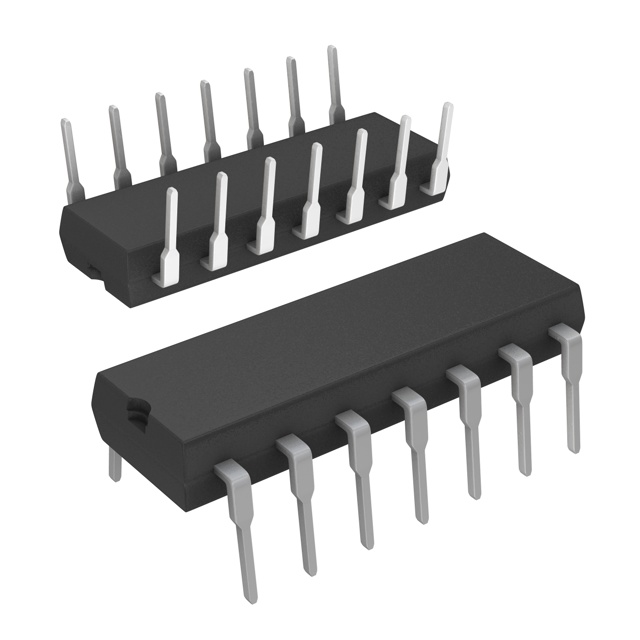
TS914IN CMOS Amplifier Equivalent & Substitute Parts
Part Overview
The TS914IN is a CMOS operational amplifier manufactured by STMicroelectronics, configured as a 4-circuit rail-to-rail amplifier in a 14-DIP package. This device is classified as obsolete, indicating discontinued production and limited availability through standard distribution channels. The TS914IN is qualified to AEC-Q100 automotive standards and operates across a wide supply voltage range of 2.7 V to 16 V with an operating temperature range of -40°C to 125°C. Identification of equivalent substitute parts is necessary due to the obsolete product status and potential supply constraints for new applications or replacement requirements.
Substiute Parts
Key Parameters
| Parameter | Value | Unit |
|---|---|---|
| Amplifier Type | CMOS | — |
| Number of Circuits | 4 | — |
| Output Type | Rail-to-Rail | — |
| Slew Rate | 1 | V/µs |
| Gain Bandwidth Product | 1.4 | MHz |
| Current - Input Bias | 1 | pA |
| Voltage - Input Offset | 10 | mV |
| Current - Supply | 230 | µA |
| Current - Output / Channel | 60 | mA |
| Voltage - Supply Span (Min) | 2.7 | V |
| Voltage - Supply Span (Max) | 16 | V |
| Operating Temperature | -40 to 125 | °C |
| Package / Case | 14-DIP (0.300", 7.62mm) | — |
| Mounting Type | Through Hole | — |
| Grade | Automotive | — |
| Qualification | AEC-Q100 | — |
Substitute Part Grouping Explanation
Substitution of the TS914IN is determined by alignment of core electrical and mechanical parameters. The primary substitution criteria are:
Functional Equivalence Parameters:
- Amplifier Type: CMOS technology
- Number of Circuits: 4 independent amplifier circuits
- Output Type: Rail-to-Rail output capability
- Gain Bandwidth Product: 1.4 MHz
- Package / Case: 14-DIP form factor with 0.300" (7.62mm) pitch
- Mounting Type: Through Hole
Operational Compatibility Parameters:
- Supply voltage range overlap
- Operating temperature range coverage
- Input bias current and input offset voltage characteristics
- Output current capability per channel
- Slew rate performance
The LMC660CN/NOPB from National Semiconductor meets the functional equivalence criteria through identical circuit count, package form factor, and core CMOS amplifier architecture. Both devices share the same 14-DIP through-hole package and deliver 1.4 MHz gain bandwidth product performance.
Parameter Comparison
| Parameter | TS914IN | LMC660CN/NOPB | Unit |
|---|---|---|---|
| Manufacturer | STMicroelectronics | National Semiconductor | — |
| Amplifier Type | CMOS | CMOS | — |
| Number of Circuits | 4 | 4 | — |
| Output Type | Rail-to-Rail | Push-Pull, Rail-to-Rail | — |
| Slew Rate | 1 | 1.1 | V/µs |
| Gain Bandwidth Product | 1.4 | 1.4 | MHz |
| Current - Input Bias | 1 | 0.002 | pA |
| Voltage - Input Offset | 10 | 1 | mV |
| Current - Supply | 230 | 1.5 (x4 Channels) | µA |
| Current - Output / Channel | 60 | 40 | mA |
| Voltage - Supply Span (Min) | 2.7 | 4.75 | V |
| Voltage - Supply Span (Max) | 16 | 15.5 | V |
| Operating Temperature | -40 to 125 | 0 to 70 | °C |
| Package / Case | 14-DIP (0.300", 7.62mm) | 14-DIP (0.300", 7.62mm) | — |
| Mounting Type | Through Hole | Through Hole | — |
| Product Status | Obsolete | Active | — |
| RoHS Status | ROHS3 Compliant | RoHS non-compliant | — |
Engineering Selection Recommendations
TS914IN Continuation: The TS914IN remains the specified component for applications requiring automotive-grade qualification (AEC-Q100), extended operating temperature range (-40°C to 125°C), and wide supply voltage operation (2.7 V to 16 V). Current inventory of 1405 pieces supports ongoing production requirements. This device is suitable for established designs where the obsolete status does not impact supply continuity.
LMC660CN/NOPB Substitution: The LMC660CN/NOPB is an active-status alternative for new designs or applications where automotive qualification is not mandatory. This substitute provides superior input bias current (0.002 pA versus 1 pA) and reduced input offset voltage (1 mV versus 10 mV), resulting in improved precision characteristics. The LMC660CN/NOPB delivers higher slew rate performance (1.1 V/µs versus 1 V/µs) and operates with reduced supply current per channel.
Substitution Constraints: The LMC660CN/NOPB operates within a narrower supply voltage range (4.75 V to 15.5 V minimum versus 2.7 V minimum for TS914IN) and restricted operating temperature range (0°C to 70°C versus -40°C to 125°C). The LMC660CN/NOPB is RoHS non-compliant, whereas the TS914IN meets ROHS3 compliance. Output current per channel is reduced to 40 mA compared to 60 mA on the TS914IN. These differences require circuit-level evaluation for compatibility in specific applications.
Frequently Asked Questions (FAQ)
Q: Can the LMC660CN/NOPB directly replace the TS914IN in existing designs?
A: Direct replacement requires verification of three critical parameters: (1) supply voltage range—the LMC660CN/NOPB minimum supply is 4.75 V, whereas TS914IN operates from 2.7 V; (2) operating temperature range—LMC660CN/NOPB is limited to 0°C to 70°C versus TS914IN's -40°C to 125°C; (3) output current per channel—LMC660CN/NOPB provides 40 mA versus TS914IN's 60 mA. Substitution is valid only when the application operates within these LMC660CN/NOPB specifications.
Q: What are the key electrical differences between these devices?
A: The LMC660CN/NOPB exhibits superior precision characteristics with input bias current of 0.002 pA (versus 1 pA) and input offset voltage of 1 mV (versus 10 mV). Slew rate is marginally higher at 1.1 V/µs. Supply current per channel is significantly lower in the LMC660CN/NOPB. Both devices share identical gain bandwidth product (1.4 MHz) and package form factor.
Q: Are both devices pin-compatible?
A: Both the TS914IN and LMC660CN/NOPB use the 14-DIP package with 0.300" (7.62mm) pitch. Pin compatibility for through-hole mounting is confirmed. However, electrical parameter differences require circuit validation before substitution.
Q: What compliance differences exist between these parts?
A: The TS914IN is AEC-Q100 qualified for automotive applications and ROHS3 compliant. The LMC660CN/NOPB is RoHS non-compliant and does not carry automotive qualification. Applications requiring automotive-grade components must retain the TS914IN.
Q: Why is the TS914IN classified as obsolete?
A: Obsolete status indicates discontinued production by STMicroelectronics. Current inventory availability (1405 pieces) supports existing applications. New designs should evaluate active alternatives such as the LMC660CN/NOPB or other current-production CMOS amplifiers meeting the required specifications.
Q: What is the impact of the narrower supply voltage range on the LMC660CN/NOPB?
A: The LMC660CN/NOPB minimum supply voltage of 4.75 V eliminates compatibility with applications operating below this threshold. The TS914IN's 2.7 V minimum enables operation in low-voltage systems. This difference is critical for battery-powered or low-supply-voltage applications.
Q: How do the input offset voltage specifications affect circuit design?
A: The TS914IN specifies 10 mV input offset voltage, while the LMC660CN/NOPB specifies 1 mV. Applications requiring precision signal conditioning benefit from the LMC660CN/NOPB's lower offset voltage. High-gain amplifier configurations or precision measurement circuits may require offset nulling with the TS914IN but operate within specification with the LMC660CN/NOPB.
Alternative Parts

SJ6012L2TP
Littelfuse Inc.
6 Alternative Parts

JMK107BBJ476MA-RE
Taiyo Yuden
10 Alternative Parts

GMK107BBJ475MA-T
Taiyo Yuden
5 Alternative Parts
SJ6020N2ARP
Littelfuse Inc.
3 Alternative Parts
SJ6025R2ATP
Littelfuse Inc.
4 Alternative Parts

2474-05L
API Delevan Inc.
1 Alternative Parts

4590R-684K
API Delevan Inc.
1 Alternative Parts

CM6560R-334
API Delevan Inc.
1 Alternative Parts

CM6460-104
API Delevan Inc.
1 Alternative Parts

5526-12
API Delevan Inc.
1 Alternative Parts