


Request Quote
(Ships tomorrow)
TS514IN Equivalent & Substitute Parts
Part Overview
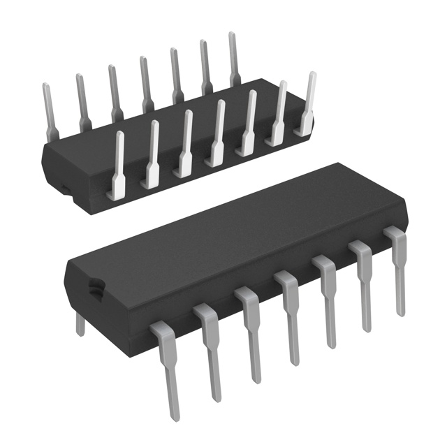
The TS514IN is a general-purpose operational amplifier integrated circuit manufactured by STMicroelectronics, configured as a 4-circuit device in a 14-DIP package. This component is classified as obsolete, indicating discontinued production and limited availability in the supply chain. The TS514IN operates across a wide supply voltage range of 6V to 30V with a gain-bandwidth product of 3 MHz and a slew rate of 1.5V/µs, making it suitable for general analog signal processing applications.
Due to its obsolete status, identifying equivalent and substitute parts is necessary for design continuity, system maintenance, and procurement planning. Substitute components must maintain functional compatibility while accommodating variations in electrical performance and operating conditions.
Substiute Parts
Key Parameters
| Parameter | TS514IN Value | Unit |
|---|---|---|
| Amplifier Type | General Purpose | — |
| Number of Circuits | 4 | — |
| Package / Case | 14-DIP (0.300", 7.62mm) | — |
| Mounting Type | Through Hole | — |
| Slew Rate | 1.5 | V/µs |
| Gain Bandwidth Product | 3 | MHz |
| Current - Input Bias | 50 | nA |
| Voltage - Input Offset | 500 | µV |
| Current - Supply | 500 | µA |
| Current - Output / Channel | 23 | mA |
| Voltage - Supply Span (Min) | 6 | V |
| Voltage - Supply Span (Max) | 30 | V |
| Operating Temperature | -40°C ~ 125°C | — |
| Product Status | Obsolete | — |
| RoHS Status | ROHS3 Compliant | — |
Substitute Part Grouping Explanation
Substitution of the TS514IN is determined by the following critical parameters:
Primary Compatibility Criteria:
- Package type: 14-DIP (0.300", 7.62mm) through-hole mounting
- Circuit count: 4 independent amplifier circuits
- Amplifier classification: General Purpose or J-FET topology
- Supply voltage range: Minimum 6V to maximum 30V overlap required
- Operating temperature range: Compatibility with -40°C to 125°C or subset thereof
Secondary Performance Criteria:
- Gain-bandwidth product: 3 MHz nominal (tolerance range acceptable)
- Slew rate: 1.5V/µs nominal (higher values acceptable for performance enhancement)
- Input bias current: 50 nA nominal (lower values acceptable)
- Output current per channel: 23 mA nominal (higher values acceptable)
Substitute parts are grouped into two categories based on amplifier topology:
Category 1: General Purpose Amplifiers — Direct functional equivalents with bipolar or CMOS input stages. These include AD704JNZ, LM2900N, LM3900N, and OP497GPZ.
Category 2: J-FET Input Amplifiers — Enhanced performance alternatives with J-FET input stages offering superior input bias current characteristics. These include TL054ACN, TL054IN, TL074BCN, and TL084BCN.
Parameter Comparison
| Parameter | TS514IN | AD704JNZ | LM2900N | LM3900N | OP497GPZ | TL054ACN | TL054IN | TL084BCN |
|---|---|---|---|---|---|---|---|---|
| Amplifier Type | General Purpose | General Purpose | General Purpose | General Purpose | General Purpose | J-FET | J-FET | J-FET |
| Number of Circuits | 4 | 4 | 4 | 4 | 4 | 4 | 4 | 4 |
| Package / Case | 14-DIP | 14-DIP | 14-DIP | 14-DIP | 14-DIP | 14-DIP | 14-DIP | 14-DIP |
| Slew Rate (V/µs) | 1.5 | 0.1 | 20 | 20 | 0.15 | 17.8 | 17.8 | 13 |
| Gain Bandwidth Product (MHz) | 3 | 0.8 | 2.5 | 2.5 | 0.5 | 2.7 | 2.7 | 3 |
| Current - Input Bias (nA/pA) | 50 nA | 100 pA | 30 nA | 30 nA | 60 pA | 30 pA | 30 pA | 30 pA |
| Voltage - Input Offset (µV) | 500 | 50 | — | — | 80 | 500 | 560 | 2000 |
| Current - Supply (µA/mA) | 500 µA | 1.5 mA | 6.2 mA | 6.2 mA | 525 µA | 8.4 mA | 8.4 mA | 1.4 mA |
| Current - Output / Channel (mA) | 23 | 15 | 18 | 10 | 25 | 80 | 80 | 10 |
| Voltage - Supply Span Min (V) | 6 | 4 | 4.4 | 4.4 | 4 | 10 | 10 | 10 |
| Voltage - Supply Span Max (V) | 30 | 36 | 32 | 32 | 40 | 30 | 30 | 30 |
| Operating Temperature (°C) | -40 ~ 125 | 0 ~ 70 | -40 ~ 85 | 0 ~ 70 | -40 ~ 85 | 0 ~ 70 | -40 ~ 85 | 0 ~ 70 |
| Product Status | Obsolete | Active | Last Time Buy | Active | Active | Last Time Buy | Last Time Buy | Active |
| RoHS Status | ROHS3 Compliant | ROHS3 Compliant | ROHS3 Compliant | ROHS3 Compliant | ROHS3 Compliant | ROHS3 Compliant | ROHS3 Compliant | ROHS3 Compliant |
Engineering Selection Recommendations
For Direct General Purpose Replacement (Minimum Design Changes):
LM3900N is the preferred substitute when maintaining the original circuit topology. This device is currently in active production status, ensuring long-term availability. It provides equivalent 4-circuit configuration in 14-DIP packaging with compatible supply voltage range (4.4V to 32V). The gain-bandwidth product of 2.5 MHz and slew rate of 20V/µs exceed the TS514IN specifications, offering performance enhancement. Operating temperature range of 0°C to 70°C covers the nominal industrial range, though it does not extend to the full -40°C to 125°C of the original part.
LM2900N serves as an alternative general-purpose substitute with active product status classified as Last Time Buy. This device offers superior slew rate (20V/µs) and extended operating temperature range (-40°C to 85°C), providing better coverage of the original temperature specification. Supply voltage compatibility spans 4.4V to 32V.
For Enhanced Performance with J-FET Input Stage:
TL084BCN is recommended when improved input bias current performance is required. This device is in active production with J-FET input topology, delivering 30 pA input bias current compared to the TS514IN's 50 nA. The 14-DIP package and 4-circuit configuration maintain mechanical compatibility. Gain-bandwidth product of 3 MHz matches the original specification exactly. Operating temperature range of 0°C to 70°C and supply voltage span of 10V to 30V provide adequate coverage for most applications.
TL054IN offers J-FET input performance with extended operating temperature range (-40°C to 85°C), though it carries Last Time Buy status. This device provides 30 pA input bias current and 2.7 MHz gain-bandwidth product.
For Low-Power Applications:
OP497GPZ provides the lowest supply current (525 µA) among available substitutes while maintaining general-purpose amplifier topology. This device supports extended supply voltage range (4V to 40V) and operating temperature range (-40°C to 85°C), offering superior environmental coverage. Output current per channel of 25 mA exceeds the TS514IN specification.
Compliance and Regulatory Considerations:
All substitute parts listed are ROHS3 compliant and REACH unaffected, maintaining regulatory alignment with the original TS514IN. All devices carry ECCN classification of EAR99 and HTSUS code 8542.33.0001, consistent with the original component.
Frequently Asked Questions (FAQ)
Q: Can I directly replace TS514IN with LM3900N without circuit modifications?
A: LM3900N is mechanically and functionally compatible as a direct pin-for-pin substitute in 14-DIP through-hole applications. Both devices provide 4 independent amplifier circuits with compatible supply voltage ranges. However, the operating temperature range differs: LM3900N operates 0°C to 70°C versus TS514IN's -40°C to 125°C. Verify that your application does not require operation below 0°C or above 70°C before substitution.
Q: What is the difference between general-purpose and J-FET input amplifiers in this comparison?
A: General-purpose amplifiers (AD704JNZ, LM2900N, LM3900N, OP497GPZ) use bipolar or CMOS input stages with input bias currents in the nanoampere range. J-FET input amplifiers (TL054ACN, TL054IN, TL084BCN) use J-FET input stages with input bias currents in the picoampere range, approximately 1000 times lower. J-FET devices are preferred for high-impedance signal sources where input bias current must be minimized. Both topologies are pin-compatible in 14-DIP packaging.
Q: Why do some substitutes have lower slew rates than the TS514IN?
A: AD704JNZ and OP497GPZ exhibit lower slew rates (0.1V/µs and 0.15V/µs respectively) due to their design optimization for low-power operation and precision applications. These devices are suitable for applications where signal bandwidth is limited and power consumption is critical. For applications requiring the original 1.5V/µs slew rate or higher, select LM2900N, LM3900N, TL054ACN, TL054IN, or TL084BCN.
Q: Are all substitute parts currently available in production?
A: Product status varies. LM3900N and TL084BCN are in active production. AD704JNZ and OP497GPZ are active. LM2900N, TL054ACN, and TL054IN carry Last Time Buy status, indicating limited future availability. For long-term supply chain planning, prioritize active production devices: LM3900N, TL084BCN, AD704JNZ, and OP497GPZ.
Q: What is the minimum supply voltage requirement for each substitute?
A: TS514IN requires minimum 6V. Substitutes vary: AD704JNZ, OP497GPZ require 4V; LM2900N, LM3900N require 4.4V; TL054ACN, TL054IN, TL084BCN require 10V. If your circuit operates at 6V to 9V, select from AD704JNZ, OP497GPZ, LM2900N, or LM3900N. For 10V and above, all substitutes are compatible.
Q: Can I use OP400GPZ as a substitute?
A: OP400GPZ is not recommended as a direct substitute. Although it provides 4 circuits in 14-DIP packaging, it features differential output configuration, which differs fundamentally from the TS514IN's standard single-ended output. Differential output devices require different circuit topology and are not pin-compatible for standard applications.
Q: What are the key parameters I should verify before substitution?
A: Verify the following parameters in your specific application: (1) Supply voltage range compatibility—ensure your circuit voltage falls within both the original and substitute device ranges; (2) Operating temperature range—confirm the substitute covers your required temperature extremes; (3) Slew rate and gain-bandwidth product—ensure the substitute meets or exceeds your signal bandwidth requirements; (4) Input bias current—critical for high-impedance applications; (5) Output current per channel—verify the substitute can drive your load impedance; (6) Package and pinout—confirm 14-DIP through-hole compatibility with your PCB layout.
Q: Is the 14-DIP package the same across all substitutes?
A: All listed substitutes use 14-DIP (0.300", 7.62mm) through-hole packaging with identical pinout, ensuring mechanical and electrical compatibility. Packaging designation may vary slightly (14-DIP versus 14-PDIP) but refers to the same physical form factor. Verify your PCB footprint accommodates 0.300" (7.62mm) row spacing.
Alternative Parts

SJ6012L2TP
Littelfuse Inc.
6 Alternative Parts

JMK107BBJ476MA-RE
Taiyo Yuden
10 Alternative Parts

GMK107BBJ475MA-T
Taiyo Yuden
5 Alternative Parts
SJ6020N2ARP
Littelfuse Inc.
3 Alternative Parts
SJ6025R2ATP
Littelfuse Inc.
4 Alternative Parts

2474-05L
API Delevan Inc.
1 Alternative Parts

4590R-684K
API Delevan Inc.
1 Alternative Parts

CM6560R-334
API Delevan Inc.
1 Alternative Parts

CM6460-104
API Delevan Inc.
1 Alternative Parts

5526-12
API Delevan Inc.
1 Alternative Parts