


Request Quote
(Ships tomorrow)
TPS61004DGS Equivalent & Substitute Parts
Part Overview
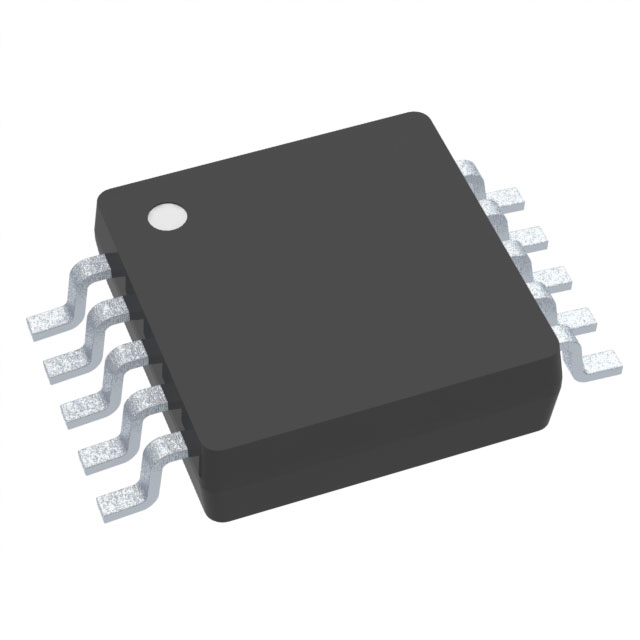
The TPS61004DGS is a boost switching regulator IC manufactured by Texas Instruments, designed for step-up voltage conversion applications. It delivers a fixed 2.8V output at 1.3A (switch current) from input voltages ranging from 0.8V to 2.8V, operating at a switching frequency of 500kHz. The device is housed in a 10-TFSOP/10-MSOP package with 0.118" width (3.00mm).
The TPS61004DGS is classified as obsolete. Identifying equivalent and substitute parts is necessary to ensure design continuity, maintain supply chain reliability, and support ongoing production or maintenance requirements for systems utilizing this component.
Substiute Parts
Key Parameters
| Parameter | Value |
|---|---|
| Function | Step-Up (Boost) |
| Output Configuration | Positive |
| Output Type | Fixed |
| Number of Outputs | 1 |
| Voltage - Input (Min) | 0.8V |
| Voltage - Input (Max) | 2.8V |
| Voltage - Output | 2.8V (Fixed) |
| Current - Output | 1.3A (Switch) |
| Frequency - Switching | 500kHz |
| Operating Temperature | -40°C ~ 85°C |
| Package / Case | 10-TFSOP, 10-MSOP (0.118", 3.00mm Width) |
| RoHS Status | ROHS3 Compliant |
| Moisture Sensitivity Level | 1 (Unlimited) |
Substitute Part Grouping Explanation
Substitution of the TPS61004DGS is determined by the following critical parameters:
- Topology: Both parts must function as boost (step-up) switching regulators
- Output Configuration: Positive output voltage required
- Package Compatibility: 10-TFSOP/10-MSOP form factor with 0.118" (3.00mm) width for PCB layout compatibility
- Output Voltage Range: The substitute must support the 2.8V output requirement within its operational range
- Input Voltage Range: The substitute must accept input voltages from 0.8V to 2.8V
- Current Capability: Output current rating must meet or exceed 1.3A (switch current)
- Compliance: RoHS3 compliance and MSL Level 1 rating required for manufacturing and storage compatibility
The LT1310EMSE#PBF from Analog Devices Inc. qualifies as a substitute based on these parameters. While it offers adjustable output voltage (versus fixed), it supports the required 2.8V output within its 2.8V to 35V range. Its 1.5A output current capability exceeds the 1.3A requirement. The package format (10-TFSOP/10-MSOP with exposed pad) maintains mechanical and electrical compatibility. Both devices are RoHS3 compliant with MSL Level 1 rating.
Parameter Comparison
| Parameter | TPS61004DGS | LT1310EMSE#PBF |
|---|---|---|
| Manufacturer | Texas Instruments | Analog Devices Inc. |
| Function | Step-Up | Step-Up |
| Output Configuration | Positive | Positive |
| Output Type | Fixed | Adjustable |
| Voltage - Input (Min) | 0.8V | 2.8V |
| Voltage - Input (Max) | 2.8V | 18V |
| Voltage - Output (Min/Fixed) | 2.8V | 2.8V |
| Voltage - Output (Max) | — | 35V |
| Current - Output | 1.3A (Switch) | 1.5A (Switch) |
| Frequency - Switching | 500kHz | 10kHz ~ 4.5MHz |
| Operating Temperature | -40°C ~ 85°C | 0°C ~ 70°C |
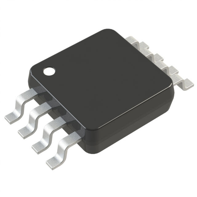
| Package / Case | 10-TFSOP, 10-MSOP (0.118", 3.00mm Width) | 10-TFSOP, 10-MSOP (0.118", 3.00mm Width) Exposed Pad |
| Product Status | Obsolete | Active |
| RoHS Status | ROHS3 Compliant | ROHS3 Compliant |
| Moisture Sensitivity Level | 1 (Unlimited) | 1 (Unlimited) |
Engineering Selection Recommendations
The LT1310EMSE#PBF is an active product from Analog Devices Inc. and serves as a functional substitute for the obsolete TPS61004DGS. Both devices are ROHS3 compliant and carry MSL Level 1 rating, ensuring compatibility with standard manufacturing and storage protocols.
Key considerations for selection:
- Product Status: The LT1310EMSE#PBF is active and in production, providing long-term supply chain stability compared to the obsolete TPS61004DGS.
- Output Voltage Configuration: The LT1310EMSE#PBF features adjustable output voltage, allowing configuration to 2.8V through external resistor networks. The TPS61004DGS provides fixed 2.8V output. Design modifications may be required to accommodate the adjustable topology.
- Input Voltage Range: The LT1310EMSE#PBF minimum input voltage is 2.8V, whereas the TPS61004DGS accepts 0.8V minimum input. Applications requiring sub-2.8V input operation cannot use the LT1310EMSE#PBF as a direct substitute.
- Operating Temperature Range: The TPS61004DGS operates from -40°C to 85°C; the LT1310EMSE#PBF operates from 0°C to 70°C. Applications requiring extended low-temperature operation below 0°C must evaluate alternative solutions.
- Current Capability: The LT1310EMSE#PBF provides 1.5A output current, exceeding the 1.3A requirement of the TPS61004DGS.
- Package Compatibility: Both devices use the same 10-TFSOP/10-MSOP footprint, enabling direct PCB layout compatibility. The LT1310EMSE#PBF includes an exposed pad for enhanced thermal performance.
Frequently Asked Questions (FAQ)
Q: Can the LT1310EMSE#PBF directly replace the TPS61004DGS without circuit modifications?
A: Direct replacement is not possible without design modifications. The LT1310EMSE#PBF requires external resistor networks to set output voltage to 2.8V, whereas the TPS61004DGS provides fixed 2.8V output. Additionally, the minimum input voltage differs: 2.8V for the LT1310EMSE#PBF versus 0.8V for the TPS61004DGS. Circuit redesign is necessary to accommodate these differences.
Q: What is the impact of the adjustable output voltage feature on design complexity?
A: The adjustable output topology of the LT1310EMSE#PBF requires external resistor dividers to establish the 2.8V output voltage. This adds component count and design complexity compared to the fixed-output TPS61004DGS. Design validation and testing are required to ensure output voltage accuracy and stability.
Q: Are there temperature range limitations when substituting the LT1310EMSE#PBF?
A: Yes. The LT1310EMSE#PBF operates from 0°C to 70°C, while the TPS61004DGS operates from -40°C to 85°C. Applications requiring operation below 0°C or above 70°C cannot use the LT1310EMSE#PBF. Alternative components must be evaluated for extended temperature applications.
Q: Is the package footprint identical between the two devices?
A: Both devices use the 10-TFSOP/10-MSOP package with 0.118" (3.00mm) width, ensuring PCB footprint compatibility. The LT1310EMSE#PBF includes an exposed pad for improved thermal management. Pin-to-pin compatibility must be verified against specific application schematics.
Q: What are the compliance and regulatory considerations?
A: Both the TPS61004DGS and LT1310EMSE#PBF are ROHS3 compliant and carry MSL Level 1 rating. Both are classified under HTSUS code 8542.39.0001 and ECCN EAR99. Compliance documentation is equivalent for both devices.
Q: What is the switching frequency difference, and does it affect circuit design?
A: The TPS61004DGS operates at a fixed 500kHz switching frequency. The LT1310EMSE#PBF operates across a range of 10kHz to 4.5MHz. This difference may affect EMI characteristics, inductor selection, and output filter design. Circuit validation is required to ensure electromagnetic compatibility and noise performance meet application requirements.
Alternative Parts

SJ6012L2TP
Littelfuse Inc.
6 Alternative Parts

JMK107BBJ476MA-RE
Taiyo Yuden
10 Alternative Parts

GMK107BBJ475MA-T
Taiyo Yuden
5 Alternative Parts
SJ6020N2ARP
Littelfuse Inc.
3 Alternative Parts
SJ6025R2ATP
Littelfuse Inc.
4 Alternative Parts

2474-05L
API Delevan Inc.
1 Alternative Parts

4590R-684K
API Delevan Inc.
1 Alternative Parts

CM6560R-334
API Delevan Inc.
1 Alternative Parts

CM6460-104
API Delevan Inc.
1 Alternative Parts

5526-12
API Delevan Inc.
1 Alternative Parts