


Request Quote
(Ships tomorrow)
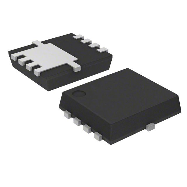
TPCC8093,L1Q N-Channel MOSFET 20V 21A Equivalent & Substitute Parts
Part Overview
The TPCC8093,L1Q is an N-Channel MOSFET manufactured by Toshiba Semiconductor and Storage, rated for 20V drain-to-source voltage with 21A continuous drain current at 25°C. This device is housed in an 8-TSON Advance (3.1x3.1) surface mount package and is classified as obsolete. Due to its obsolete product status and limited availability in future procurement cycles, identifying equivalent substitute components is essential for design continuity and long-term supply chain management.
Substiute Parts
Key Parameters
| Parameter | Value | Unit |
|---|---|---|
| FET Type | N-Channel | — |
| Technology | MOSFET (Metal Oxide) | — |
| Drain to Source Voltage (Vdss) | 20 | V |
| Current - Continuous Drain (Id) @ 25°C | 21 | A (Ta) |
| Rds On (Max) @ Id, Vgs | 5.8 mOhm @ 10.5A, 4.5V | — |
| Vgs(th) (Max) @ Id | 1.2 | V @ 500µA |
| Gate Charge (Qg) (Max) @ Vgs | 16 | nC @ 5V |
| Vgs (Max) | ±12 | V |
| Input Capacitance (Ciss) (Max) @ Vds | 1860 | pF @ 10V |
| Power Dissipation (Max) | 1.9 (Ta), 30 (Tc) | W |
| Operating Temperature | 150 | °C |
| Mounting Type | Surface Mount | — |
| Package / Case | 8-PowerVDFN | — |
| RoHS Status | RoHS Compliant | — |
Substitute Part Grouping Explanation
Substitution of the TPCC8093,L1Q is determined by strict electrical and mechanical compatibility criteria. The following parameters establish the substitution basis:
Electrical Compatibility Requirements:
- Drain-to-Source Voltage (Vdss) must equal or exceed 20V
- Continuous Drain Current (Id) at 25°C must meet or exceed 21A (Ta)
- Gate threshold voltage (Vgs(th)) must be compatible with 1.2V maximum specification
- Maximum gate voltage (Vgs) must support ±12V operation
- On-state resistance (Rds On) characteristics must be within acceptable operating parameters
Mechanical Compatibility Requirements:
- Surface mount technology required
- Package footprint must be compatible with 8-pin configurations
- Environmental compliance must meet RoHS standards
The BSC046N02KSGAUMA1 from Infineon Technologies satisfies these criteria with equivalent Vdss (20V), comparable continuous drain current (19A Ta), matching gate voltage specifications, and RoHS3 compliance. Both devices operate within the same voltage and current envelope, enabling direct functional substitution in circuit applications.
Parameter Comparison
| Parameter | TPCC8093,L1Q (Toshiba) | BSC046N02KSGAUMA1 (Infineon) | Unit |
|---|---|---|---|
| FET Type | N-Channel | N-Channel | — |
| Technology | MOSFET (Metal Oxide) | MOSFET (Metal Oxide) | — |
| Drain to Source Voltage (Vdss) | 20 | 20 | V |
| Current - Continuous Drain (Id) @ 25°C | 21 (Ta) | 19 (Ta), 80 (Tc) | A |
| Rds On (Max) @ Id, Vgs | 5.8 mOhm @ 10.5A, 4.5V | 4.6 mOhm @ 50A, 4.5V | — |
| Vgs(th) (Max) @ Id | 1.2 @ 500µA | 1.2 @ 110µA | V |
| Gate Charge (Qg) (Max) @ Vgs | 16 @ 5V | 27.6 @ 4.5V | nC |
| Vgs (Max) | ±12 | ±12 | V |
| Input Capacitance (Ciss) (Max) @ Vds | 1860 @ 10V | 4100 @ 10V | pF |
| Power Dissipation (Max) | 1.9 (Ta), 30 (Tc) | 2.8 (Ta), 48 (Tc) | W |
| Operating Temperature (Max) | 150 | 150 (TJ) | °C |
| Mounting Type | Surface Mount | Surface Mount | — |
| RoHS Status | RoHS Compliant | ROHS3 Compliant | — |
Engineering Selection Recommendations
TPCC8093,L1Q (Toshiba) — Primary Part (Obsolete Status)
The TPCC8093,L1Q is classified as obsolete and carries a product status indicating end-of-life. While 6040 pieces are currently in stock, this part is not recommended for new designs or long-term production commitments. RoHS compliance is confirmed. This part should be used only for legacy system maintenance or existing inventory replenishment where design changes are not feasible.
BSC046N02KSGAUMA1 (Infineon) — Recommended Substitute
The BSC046N02KSGAUMA1 is classified as Last Time Buy, indicating controlled availability with a defined end-of-support window. This part provides superior electrical performance characteristics, including lower on-state resistance (4.6 mOhm vs. 5.8 mOhm) and higher power dissipation capability (48W Tc vs. 30W Tc). ROHS3 compliance and REACH Unaffected status confirm environmental and regulatory alignment. The substitute meets all critical electrical parameters: equivalent 20V Vdss rating, comparable continuous drain current (19A Ta), matching gate voltage specifications (±12V, 1.2V threshold), and surface mount compatibility. The higher gate charge (27.6 nC vs. 16 nC) and input capacitance (4100 pF vs. 1860 pF) require circuit-level evaluation for switching speed and driver capability, but do not preclude substitution in standard applications.
For new designs and production transitions, the BSC046N02KSGAUMA1 is the appropriate selection. For existing designs using the TPCC8093,L1Q, substitution is electrically and mechanically viable with standard circuit validation.
Frequently Asked Questions (FAQ)
Q: Can the BSC046N02KSGAUMA1 directly replace the TPCC8093,L1Q in existing designs?
A: Direct substitution is electrically and mechanically feasible. Both devices share identical Vdss (20V) and Vgs specifications (±12V, 1.2V threshold). Continuous drain current ratings are comparable (21A vs. 19A at Ta). The primary design consideration is the higher gate charge (27.6 nC vs. 16 nC) and input capacitance (4100 pF vs. 1860 pF) of the substitute, which may require gate driver capability verification. On-state resistance is improved in the substitute (4.6 mOhm vs. 5.8 mOhm), reducing power dissipation. Standard circuit validation is required before production implementation.
Q: What are the package compatibility considerations?
A: The TPCC8093,L1Q uses an 8-TSON Advance (3.1x3.1) package (8-PowerVDFN case). The BSC046N02KSGAUMA1 uses a PG-TDSON-8-1 package (8-PowerTDFN case). Both are 8-pin surface mount packages with similar footprints and pin configurations. PCB layout verification is required to confirm mechanical fit, thermal pad alignment, and trace routing compatibility. Consult package datasheets for precise dimensional specifications.
Q: Why does the substitute have higher gate charge and input capacitance?
A: The BSC046N02KSGAUMA1 exhibits higher gate charge (27.6 nC vs. 16 nC) and input capacitance (4100 pF vs. 1860 pF) due to differences in semiconductor process technology and die design between Toshiba and Infineon. These parameters affect gate driver requirements and switching speed. Higher values require gate drivers with adequate current sourcing capability. This does not indicate inferior performance but reflects different design optimization priorities. Verify gate driver specifications against the substitute's requirements.
Q: What is the significance of the product status classifications?
A: The TPCC8093,L1Q is classified as obsolete, indicating Toshiba has discontinued production and support. The BSC046N02KSGAUMA1 is classified as Last Time Buy, indicating Infineon has announced end-of-life with a defined final order date. For new designs, neither part is recommended for long-term production. However, the BSC046N02KSGAUMA1 provides a transition path with controlled availability. For legacy system support, the TPCC8093,L1Q remains available from current inventory (6040 pieces).
Q: Are there compliance differences between the two parts?
A: The TPCC8093,L1Q is RoHS Compliant. The BSC046N02KSGAUMA1 is ROHS3 Compliant and REACH Unaffected. ROHS3 represents the current RoHS directive revision with updated substance restrictions. Both parts meet environmental compliance requirements for EU and global markets. The substitute provides enhanced regulatory alignment with current standards.
Q: How do the thermal characteristics compare?
A: The TPCC8093,L1Q is rated for 1.9W (Ta) and 30W (Tc) power dissipation. The BSC046N02KSGAUMA1 is rated for 2.8W (Ta) and 48W (Tc). The substitute provides superior thermal performance, particularly under case temperature conditions (Tc), enabling higher power handling capability. Both devices support 150°C maximum operating temperature. Thermal management design should account for the improved dissipation capability of the substitute.
Alternative Parts

SJ6012L2TP
Littelfuse Inc.
6 Alternative Parts

JMK107BBJ476MA-RE
Taiyo Yuden
10 Alternative Parts

GMK107BBJ475MA-T
Taiyo Yuden
5 Alternative Parts
SJ6020N2ARP
Littelfuse Inc.
3 Alternative Parts
SJ6025R2ATP
Littelfuse Inc.
4 Alternative Parts

2474-05L
API Delevan Inc.
1 Alternative Parts

4590R-684K
API Delevan Inc.
1 Alternative Parts

CM6560R-334
API Delevan Inc.
1 Alternative Parts

CM6460-104
API Delevan Inc.
1 Alternative Parts

5526-12
API Delevan Inc.
1 Alternative Parts