


Request Quote
(Ships tomorrow)
TLV5639CDWR Equivalent & Substitute Parts
Part Overview
The TLV5639CDWR is a 12-bit digital-to-analog converter (DAC) manufactured by Texas Instruments, designed for data acquisition applications requiring voltage output buffering. This device features a single DAC channel with parallel data interface, supporting both external and internal reference configurations across dual supply voltage ranges (2.7V–3.3V and 5V).
The TLV5639CDWR is classified as obsolete. Locating equivalent or substitute components is necessary to ensure design continuity, maintain supply chain reliability, and support long-term product availability for applications currently utilizing this part.
Substiute Parts
Key Parameters
| Parameter | Value |
|---|---|
| Manufacturer | Texas Instruments |
| Category | Data Acquisition |
| Number of Bits | 12 |
| Number of D/A Converters | 1 |
| Output Type | Voltage - Buffered |
| Data Interface | Parallel |
| Reference Type | External, Internal |
| Voltage - Supply, Analog | 2.7V ~ 3.3V, 5V |
| Voltage - Supply, Digital | 2.7V ~ 3.3V, 5V |
| Settling Time | 7µs |
| INL/DNL (LSB) | ±1.2, ±0.3 |
| Architecture | String DAC |
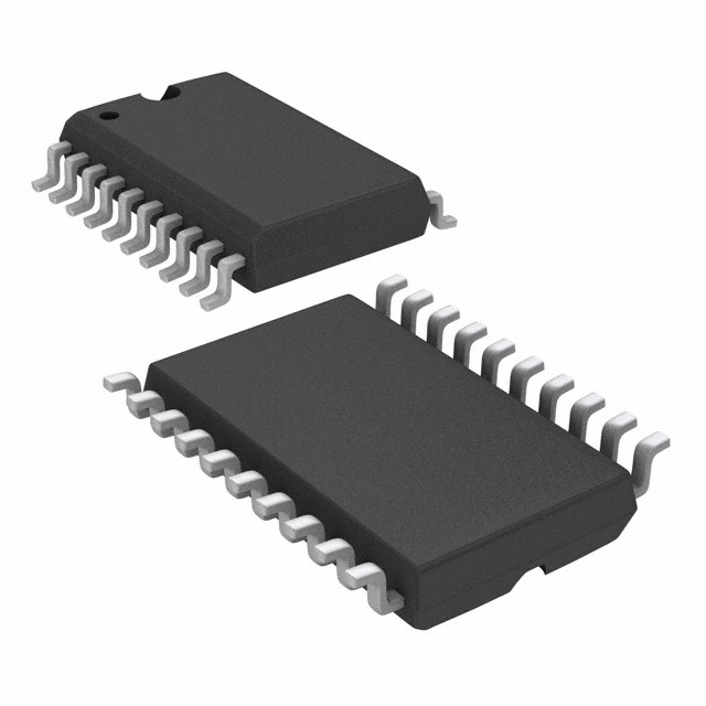
| Package / Case | 20-SOIC (0.295", 7.50mm Width) |
| Mounting Type | Surface Mount |
| RoHS Status | ROHS3 Compliant |
| Moisture Sensitivity Level (MSL) | 1 (Unlimited) |
Substitute Part Grouping Explanation
Substitution of the TLV5639CDWR is determined by strict equivalence across the following critical parameters:
- Resolution and Channel Count: 12-bit resolution with single DAC channel
- Output Configuration: Voltage output with buffering capability
- Data Interface: Parallel interface architecture
- Reference Configuration: Support for both external and internal reference types
- Supply Voltage Ranges: Dual supply operation at 2.7V–3.3V and 5V for both analog and digital supplies
- Settling Time: 7µs maximum settling time
- Linearity Specifications: INL/DNL performance of ±1.2 LSB and ±0.3 LSB respectively
- Package Compatibility: 20-SOIC surface mount package with identical physical dimensions
- Compliance Standards: ROHS3 compliance and MSL Level 1 rating
The TLV5639IDW meets all these criteria and qualifies as a direct substitute for the TLV5639CDWR.
Parameter Comparison
| Parameter | TLV5639CDWR (Main Part) | TLV5639IDW (Substitute) |
|---|---|---|
| Manufacturer | Texas Instruments | Texas Instruments |
| Product Status | Obsolete | Active |
| Number of Bits | 12 | 12 |
| Number of D/A Converters | 1 | 1 |
| Output Type | Voltage - Buffered | Voltage - Buffered |
| Data Interface | Parallel | Parallel |
| Reference Type | External, Internal | External, Internal |
| Voltage - Supply, Analog | 2.7V ~ 3.3V, 5V | 2.7V ~ 3.3V, 5V |
| Voltage - Supply, Digital | 2.7V ~ 3.3V, 5V | 2.7V ~ 3.3V, 5V |
| Settling Time | 7µs | 7µs |
| INL/DNL (LSB) | ±1.2, ±0.3 | ±1.2, ±0.3 |
| Architecture | String DAC | String DAC |
| Operating Temperature | 0°C ~ 70°C | -40°C ~ 85°C |
| Package / Case | 20-SOIC (0.295", 7.50mm Width) | 20-SOIC (0.295", 7.50mm Width) |
| Mounting Type | Surface Mount | Surface Mount |
| RoHS Status | ROHS3 Compliant | ROHS3 Compliant |
| Moisture Sensitivity Level (MSL) | 1 (Unlimited) | 1 (Unlimited) |
Engineering Selection Recommendations
The TLV5639IDW is the direct substitute for the obsolete TLV5639CDWR. Both parts maintain identical electrical specifications, package geometry, and compliance certifications (ROHS3, MSL Level 1). The substitute part is currently in active production status, ensuring supply chain availability.
The primary difference between the two parts is the operating temperature range. The TLV5639CDWR operates from 0°C to 70°C, while the TLV5639IDW extends operation to -40°C to 85°C. This expanded temperature range in the substitute part provides additional design flexibility for applications requiring extended environmental performance without compromising any electrical or functional characteristics.
Both parts are REACH unaffected and carry identical ECCN and HTSUS classifications, supporting regulatory compliance requirements across international markets.
Frequently Asked Questions (FAQ)
Q: Can the TLV5639IDW directly replace the TLV5639CDWR in existing designs?
A: Yes. The TLV5639IDW is electrically and mechanically identical to the TLV5639CDWR. Both parts feature the same 12-bit resolution, settling time, linearity specifications, supply voltage ranges, and 20-SOIC package configuration. No circuit modifications are required for substitution.
Q: What is the key difference between these two parts?
A: The operating temperature range differs. The TLV5639CDWR operates from 0°C to 70°C, while the TLV5639IDW operates from -40°C to 85°C. The substitute part supports a wider temperature envelope, making it suitable for applications requiring extended environmental performance.
Q: Are there any compliance or certification differences?
A: No. Both parts maintain identical ROHS3 compliance, MSL Level 1 rating, REACH unaffected status, and equivalent ECCN and HTSUS classifications. Regulatory requirements are satisfied equally by either part.
Q: Why is the TLV5639CDWR classified as obsolete?
A: The TLV5639CDWR has reached end-of-life status in Texas Instruments' product portfolio. The TLV5639IDW represents the active production equivalent, ensuring continued availability and supply chain support for applications requiring this functionality.
Q: Is the 20-SOIC package identical between both parts?
A: Yes. Both the TLV5639CDWR and TLV5639IDW use the same 20-SOIC package with 0.295" (7.50mm) width. PCB footprints, component placement, and mechanical clearances are identical, supporting direct board-level substitution.
Q: Do both parts support the same reference voltage configurations?
A: Yes. Both parts support external and internal reference types with identical supply voltage ranges of 2.7V–3.3V and 5V for analog and digital supplies. Reference circuit design remains unchanged between the two parts.
Alternative Parts

SJ6012L2TP
Littelfuse Inc.
6 Alternative Parts

JMK107BBJ476MA-RE
Taiyo Yuden
10 Alternative Parts

GMK107BBJ475MA-T
Taiyo Yuden
5 Alternative Parts
SJ6020N2ARP
Littelfuse Inc.
3 Alternative Parts
SJ6025R2ATP
Littelfuse Inc.
4 Alternative Parts

2474-05L
API Delevan Inc.
1 Alternative Parts

4590R-684K
API Delevan Inc.
1 Alternative Parts

CM6560R-334
API Delevan Inc.
1 Alternative Parts

CM6460-104
API Delevan Inc.
1 Alternative Parts

5526-12
API Delevan Inc.
1 Alternative Parts