


Request Quote
(Ships tomorrow)
TLV2623IDGS Equivalent & Substitute Parts
Part Overview
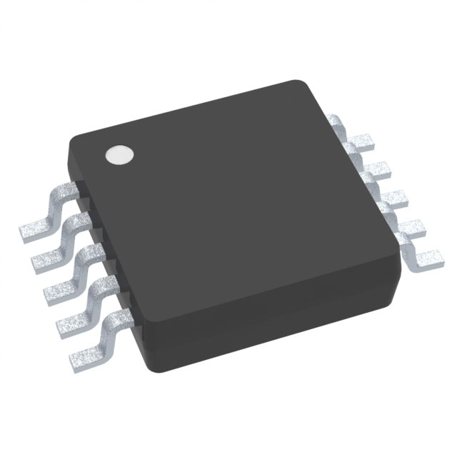
The TLV2623IDGS is a CMOS dual-channel operational amplifier manufactured by Texas Instruments, designed for rail-to-rail signal conditioning applications. This device integrates two independent amplifier circuits in a 10-VSSOP surface mount package, suitable for low-power analog signal processing across supply voltages from 2.7 V to 5.5 V.
The TLV2623IDGS is designated as Last Time Buy, indicating discontinued production status. Identification of functionally compatible substitute components is necessary for ongoing design support and procurement continuity.
Substiute Parts
Key Parameters
| Parameter | Value | Unit |
|---|---|---|
| Amplifier Type | CMOS | — |
| Number of Circuits | 2 | Channels |
| Output Type | Rail-to-Rail | — |
| Slew Rate | 7 | V/µs |
| Gain Bandwidth Product | 11 | MHz |
| Current - Input Bias | 2 | pA |
| Voltage - Input Offset | 250 | µV |
| Current - Supply (per 2 Channels) | 800 | µA |
| Current - Output / Channel | 28 | mA |
| Voltage - Supply Span (Min) | 2.7 | V |
| Voltage - Supply Span (Max) | 5.5 | V |
| Operating Temperature | -40 to 125 | °C |
| Package / Case | 10-TFSOP, 10-MSOP (0.118", 3.00mm Width) | — |
| Mounting Type | Surface Mount | — |
| RoHS Status | ROHS3 Compliant | — |
| Moisture Sensitivity Level (MSL) | 1 (Unlimited) | — |
Substitute Part Grouping Explanation
Substitution of the TLV2623IDGS is determined by equivalence across the following critical parameters:
Functional Equivalence Criteria:
- Amplifier topology: CMOS technology
- Circuit count: Dual-channel (2 circuits)
- Output configuration: Rail-to-rail operation
- Package form factor: 10-VSSOP surface mount
- Supply voltage range: Minimum 2.7 V, maximum 5.5 V
- Operating temperature range: -40°C to 125°C
- Regulatory compliance: ROHS3 and REACH status
Performance Compatibility Boundaries: Substitute parts must maintain functional compatibility within the electrical operating envelope defined by the main part's slew rate, gain bandwidth product, input bias current, input offset voltage, supply current, and output current specifications. Variations in these parameters are acceptable provided the substitute part operates within the application's design margins.
The TLV9062SIDGSR qualifies as a direct substitute based on matching package geometry, supply voltage range, temperature rating, and regulatory compliance status, with documented variations in performance characteristics within acceptable engineering tolerances.
Parameter Comparison
| Parameter | TLV2623IDGS (Main Part) | TLV9062SIDGSR (Substitute) | Unit |
|---|---|---|---|
| Manufacturer | Texas Instruments | Texas Instruments | — |
| Amplifier Type | CMOS | CMOS | — |
| Number of Circuits | 2 | 2 | Channels |
| Output Type | Rail-to-Rail | Rail-to-Rail | — |
| Slew Rate | 7 | 6.5 | V/µs |
| Gain Bandwidth Product | 11 | 10 | MHz |
| Current - Input Bias | 2 | 0.5 | pA |
| Voltage - Input Offset | 250 | 300 | µV |
| Current - Supply (per 2 Channels) | 800 | 538 | µA |
| Current - Output / Channel | 28 | 50 | mA |
| Voltage - Supply Span (Min) | 2.7 | 1.8 | V |
| Voltage - Supply Span (Max) | 5.5 | 5.5 | V |
| Operating Temperature | -40 to 125 | -40 to 125 | °C |
| Package / Case | 10-TFSOP, 10-MSOP (0.118", 3.00mm Width) | 10-TFSOP, 10-MSOP (0.118", 3.00mm Width) | — |
| Mounting Type | Surface Mount | Surface Mount | — |
| Product Status | Last Time Buy | Active | — |
| RoHS Status | ROHS3 Compliant | ROHS3 Compliant | — |
| Moisture Sensitivity Level (MSL) | 1 (Unlimited) | 2 (1 Year) | — |
Engineering Selection Recommendations
Product Status Consideration: The TLV2623IDGS is designated Last Time Buy, indicating end-of-life status with no further production planned. The TLV9062SIDGSR maintains Active product status with current manufacturing availability, supporting long-term supply chain continuity.
Compliance and Certification: Both parts maintain ROHS3 compliance and REACH unaffected status, satisfying regulatory requirements for equivalent applications. The TLV9062SIDGSR carries MSL Level 2 (1 Year) moisture sensitivity rating compared to MSL Level 1 (Unlimited) for the TLV2623IDGS, requiring appropriate moisture control during storage and handling per IPC-A-610 standards.
Supply Voltage Range: The TLV9062SIDGSR extends the minimum supply voltage specification to 1.8 V, providing broader operational flexibility compared to the TLV2623IDGS minimum of 2.7 V. Both devices support the maximum 5.5 V supply specification.
Performance Characteristics: The TLV9062SIDGSR demonstrates lower input bias current (0.5 pA versus 2 pA) and reduced supply current consumption (538 µA versus 800 µA per dual channels), while providing increased output current capability (50 mA versus 28 mA per channel). Slew rate and gain bandwidth product are marginally lower, remaining within typical application tolerances for general-purpose signal conditioning.
Frequently Asked Questions (FAQ)
Q: Can the TLV9062SIDGSR directly replace the TLV2623IDGS in existing PCB designs?
A: Yes. Both devices share identical package geometry (10-VSSOP, 10-TFSOP, 10-MSOP with 0.118" / 3.00mm width), identical pin configuration, and compatible electrical operating ranges. PCB layout and footprints require no modification. Schematic symbol compatibility is maintained.
Q: What are the key electrical differences between these parts?
A: The TLV9062SIDGSR provides lower input bias current (0.5 pA versus 2 pA), reduced supply current (538 µA versus 800 µA), and higher output current per channel (50 mA versus 28 mA). Slew rate is 6.5 V/µs versus 7 V/µs, and gain bandwidth product is 10 MHz versus 11 MHz. Input offset voltage is 300 µV versus 250 µV. These variations remain within acceptable engineering tolerances for most applications.
Q: Does the TLV9062SIDGSR support the same supply voltage range?
A: The TLV9062SIDGSR extends the minimum supply voltage to 1.8 V, compared to 2.7 V for the TLV2623IDGS. Both support maximum 5.5 V operation. Applications operating at 2.7 V or higher are fully compatible with both devices.
Q: What is the significance of the different MSL ratings?
A: The TLV2623IDGS carries MSL Level 1 (Unlimited moisture sensitivity), while the TLV9062SIDGSR carries MSL Level 2 (1 Year). MSL Level 2 requires moisture control during storage and handling. Components must be stored in dry conditions and baked per IPC-A-610 guidelines prior to reflow soldering if moisture absorption occurs.
Q: Are both parts RoHS and REACH compliant?
A: Yes. Both the TLV2623IDGS and TLV9062SIDGSR are ROHS3 compliant and REACH unaffected, meeting regulatory requirements for equivalent applications in restricted substance directives.
Q: What is the availability status of each part?
A: The TLV2623IDGS is Last Time Buy (discontinued production). The TLV9062SIDGSR maintains Active product status with current manufacturing and distribution support, ensuring long-term procurement availability.
Alternative Parts

SJ6012L2TP
Littelfuse Inc.
6 Alternative Parts

JMK107BBJ476MA-RE
Taiyo Yuden
10 Alternative Parts

GMK107BBJ475MA-T
Taiyo Yuden
5 Alternative Parts
SJ6020N2ARP
Littelfuse Inc.
3 Alternative Parts
SJ6025R2ATP
Littelfuse Inc.
4 Alternative Parts

2474-05L
API Delevan Inc.
1 Alternative Parts

4590R-684K
API Delevan Inc.
1 Alternative Parts

CM6560R-334
API Delevan Inc.
1 Alternative Parts

CM6460-104
API Delevan Inc.
1 Alternative Parts

5526-12
API Delevan Inc.
1 Alternative Parts